EP4073661B1 - Récupération de données et d'horloge à demi-fréquence en boucle ouverte très rapide pour des interfaces de couches physiques (c-phy) de prochaine génération - Google Patents
Récupération de données et d'horloge à demi-fréquence en boucle ouverte très rapide pour des interfaces de couches physiques (c-phy) de prochaine génération Download PDFInfo
- Publication number
- EP4073661B1 EP4073661B1 EP20807235.5A EP20807235A EP4073661B1 EP 4073661 B1 EP4073661 B1 EP 4073661B1 EP 20807235 A EP20807235 A EP 20807235A EP 4073661 B1 EP4073661 B1 EP 4073661B1
- Authority
- EP
- European Patent Office
- Prior art keywords
- signal
- state
- symbol
- delay
- clock
- Prior art date
- Legal status (The legal status is an assumption and is not a legal conclusion. Google has not performed a legal analysis and makes no representation as to the accuracy of the status listed.)
- Active
Links
Images








Classifications
-
- H—ELECTRICITY
- H04—ELECTRIC COMMUNICATION TECHNIQUE
- H04L—TRANSMISSION OF DIGITAL INFORMATION, e.g. TELEGRAPHIC COMMUNICATION
- H04L7/00—Arrangements for synchronising receiver with transmitter
- H04L7/02—Speed or phase control by the received code signals, the signals containing no special synchronisation information
- H04L7/033—Speed or phase control by the received code signals, the signals containing no special synchronisation information using the transitions of the received signal to control the phase of the synchronising-signal-generating means, e.g. using a phase-locked loop
-
- G—PHYSICS
- G06—COMPUTING OR CALCULATING; COUNTING
- G06F—ELECTRIC DIGITAL DATA PROCESSING
- G06F13/00—Interconnection of, or transfer of information or other signals between, memories, input/output devices or central processing units
- G06F13/38—Information transfer, e.g. on bus
- G06F13/42—Bus transfer protocol, e.g. handshake; Synchronisation
- G06F13/4265—Bus transfer protocol, e.g. handshake; Synchronisation on a point to point bus
- G06F13/4278—Bus transfer protocol, e.g. handshake; Synchronisation on a point to point bus using an embedded synchronisation
-
- H—ELECTRICITY
- H04—ELECTRIC COMMUNICATION TECHNIQUE
- H04L—TRANSMISSION OF DIGITAL INFORMATION, e.g. TELEGRAPHIC COMMUNICATION
- H04L7/00—Arrangements for synchronising receiver with transmitter
- H04L7/0016—Arrangements for synchronising receiver with transmitter correction of synchronization errors
- H04L7/0033—Correction by delay
- H04L7/0037—Delay of clock signal
Definitions
- the feedback loop may be used to ensure that pulse generating circuits do not generate additional pulses triggered by transients that can occur before the conductors in the trio have assumed a stable signaling state before providing a sampling edge.
- Maximum symbol transmission rate may be limited by the feedback loop, and there is an ongoing need for optimized clock generation circuits that can function reliably at ever-higher signaling frequencies.
- a clock recovery apparatus has a plurality of pulse generating circuits, a first logic circuit and a delay flipflop.
- Each pulse generating circuit is configured to generate a transition pulse in response to a transition in one of three difference signals representative of a difference in signaling state of a pair of wires in a three-wire bus. Transitions in one or more difference signals can occur at boundaries between symbols that are sequentially transmitted over the three-wire bus.
- the first logic circuit is configured to provide a single pulse in a combination signal at each boundary between pairs of sequentially-transmitted symbols by combining one or more transition pulses received from the plurality of pulse generating circuits.
- the delay flipflop is configured to respond to each pulse in the combination signal by changing signaling state of a clock signal that is output by the clock recovery apparatus. The symbols may be sequentially transmitted over the three-wire bus in accordance with a C-PHY protocol.
- Examples of a mobile apparatus include a mobile computing device, a cellular phone, a smart phone, a session initiation protocol (SIP) phone, a laptop, a notebook, a netbook, a smartbook, a personal digital assistant (PDA), a satellite radio, a global positioning system (GPS) device, a smart home device, intelligent lighting, a multimedia device, a video device, a digital audio player (e.g., MP3 player), a camera, a game console, an entertainment device, a vehicle component, avionics systems, a wearable computing device (e.g., a smartwatch, a health or fitness tracker, eyewear, etc.), an appliance, a sensor, a security device, a vending machine, a smart meter, a drone, a multicopter, or any other similarly functioning device.
- a mobile computing device e.g., a smartwatch, a health or fitness tracker, eyewear, etc.
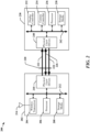
- the processing circuit 102 may provide one or more buses 118a, 118b, 120 that enable certain devices 104, 106, and/or 108 to communicate.
- the ASIC 104 may include a bus interface circuit 116 that includes a combination of circuits, counters, timers, control logic and other configurable circuits or modules.
- the bus interface circuit 116 may be configured to operate in accordance with communication specifications or protocols.
- the processing circuit 102 may include or control a power management function that configures and manages the operation of the apparatus 100.
- the display controller 232 may include circuits and software drivers that support displays such as a liquid crystal display (LCD) panel, touch-screen display, indicators and so on.
- the storage media 208 and 238 may include transitory and/or non-transitory storage devices adapted to maintain instructions and data used by respective processors 206 and 236, and/or other components of the IC devices 202 and 230. Communication between each processor 206, 236 and its corresponding storage media 208 and 238 and other modules and circuits may be facilitated by one or more internal buses 212 and 242 and/or a channel 222, 224 and/or 226 of the communication link 220.
- a 3-wire, 3-phase polarity encoder may employ line drivers 308 to control the signaling state of signal wires 318a, 318b and 318c.
- the line drivers 308 may be implemented as unit-level current-mode or voltage-mode drivers.
- each line driver 308 may receive sets of signals 316a, 316b and 316c that determine the output state of corresponding signal wires 318a, 318b and 318c.
- M-wire, N-phase encoding permits a number of bits to be encoded in a plurality of symbols where the bits per symbol is not an integer.
- FIG. 4 includes an example of a timing chart 400 for signals encoded using a three-phase modulation data-encoding scheme, which is based on the circular state diagram 450.
- Information may be encoded in a sequence of signaling states where, for example, a wire or connector is in one of three phase states S 1 , S 2 and S 3 defined by the circular state diagram 450. Each state may be separated from the other states by a 120° phase shift.
- data may be encoded in the direction of rotation of phase states on the wire or connector.
- the phase states in a signal may rotate in clockwise direction 452 and 452' or counterclockwise direction 454 and 454'.
- the timing chart 400 illustrates data encoding using both phase rotation direction and polarity.
- the curves 402, 404 and 406 relate to signals carried on three signal wires 318a, 318b and 318c, respectively for multiple phase states.
- the phase transitions 410 are in a clockwise direction and the most significant bit is set to binary '1,' until the rotation of phase transitions 410 switches at a time 414 to a counterclockwise direction, as represented by a binary '0' of the most significant bit.
- the least significant bit reflects the polarity 408 of the signal in each state.
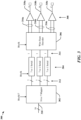
- FIG. 5 is a diagram illustrating certain aspects of a 3-wire, 3-phase decoder 500.
- Differential receivers 502a, 502b, 502c and a wire state decoder 504 are configured to provide a digital representation 522 of the state of the three transmission lines (e.g., the signal wires 318a, 318b and 318c illustrated in FIG. 3 ), with respect to one another, and to detect changes in the state of the three transmission lines compared to the state transmitted in the previous symbol period. Seven consecutive states are assembled by the serial-to-parallel convertors 506 to obtain a set of 7 symbols 516 to be processed by the demapper 508.
- the demapper 508 produces 16 bits of data 518 that may be buffered in a first-in-first-out (FIFO) register 510 to provide output data 520.
- FIFO first-in-first-out
- the transitions in the state diagram 600 can be represented by a Flip, Rotate, Polarity symbol (e.g., the FRP symbol 626) that has one of the three-bit binary values in the set: ⁇ 000, 001, 010, 011, 100 ⁇ .
- the Rotation bit 622 of the FRP symbol 626 indicates the direction of phase rotation associated with a transition to a next state.
- the Polarity bit 624 of the FRP symbol 626 is set to binary 1 when a transition to a next state involves a change in polarity.
- the Flip bit 620 of the FRP symbol 626 is set to binary 1, the Rotate and Polarity values may be ignored and/or zeroed.
- a flip represents a state transition that involves only a change in polarity.
- the second symbol interval may end at time 726 when a third symbol Sym n +2 706 is transmitted in the third symbol interval, which ends when a fourth symbol Sym n +3 708 is transmitted in a fourth symbol interval.
- the transition from a state determined by the first symbol 702 to the state corresponding to the second symbol 704 may be detectable after a delay 712 attributable to the time taken for voltage in the signal wire 318a, 318b or 318c to reach a threshold voltage 718 and/or 720.
- the threshold voltages may be used to determine the state of the signal wire 318a, 318b or 318c.
- a first differential receiver 802a provides an AB difference signal 810a representative of the difference in signaling state of A and B signal wires 318a and 318b
- a second differential receiver 802b provides a BC difference signal 810b representative of the difference in signaling state of B and C signal wires 318b and 318c
- a third differential receiver 802c provides a CA difference signal 810c representative of the difference in signaling state of C and A signal wires 318c and 318a.
- a transition detection circuit 804 can be configured to detect occurrence of a phase change because the output of at least one of the differential receivers 802a, 802b and 802c changes at the end of each symbol interval.
- a clock generation circuit 806 may include a transition detection circuit 804 and/or other logic to monitor the outputs of all differential receivers 802a, 802b and 802c in order to determine when a phase transition has occurred.
- the clock generation circuit generates a receive clock signal 808 based on detected phase transitions.
- Changes in signaling states of the 3 wires in a trio may be detected at different times, which can result in the difference signals 810a, 810b, 810c assuming stable states at different times.
- the state of the difference signals 810a, 810b, 810c may switch before stability has been reached after the signaling state of each signal wire 318a, 318b and/or 318c has transitioned to its defined state for a symbol transmission interval. The result of such variability is illustrated in the timing diagram 820 of FIG. 8 .
- the timing of signaling state change detection may vary according to the type of signaling state change that has occurred.
- Markers 822, 824 and 826 represent occurrences of transitions in the difference signals 810a, 810b, 810c provided to the transition detection circuit 804.
- the markers 822, 824 and 826 are assigned different heights in the timing diagram 820 for clarity of illustration only, and the relative heights of the markers 822, 824 and 826 are not intended to show a specific relationship to voltage or current levels, polarity or weighting values used for clock generation or data decoding.
- the timing diagram 820 illustrates the effect of timing of transitions associated with symbols transmitted in phase and polarity on the three signal wires 318a, 318b and 318c.
- the throughput of a C-PHY communication link may be affected by duration and variability in signal transition times.
- variability in detection circuits may be caused by manufacturing process tolerances, variations and stability of voltage and current sources and operating temperature, as well as by the electrical characteristics of the signal wires 318a, 318b and 318c.
- the variability in detection circuits may limit channel bandwidth.
- FIG. 9 includes timing diagrams 900 and 920 representative of certain examples of transitions from a first signaling state to a second signaling state between certain consecutive symbols.
- the signaling state transitions illustrated in the timing diagrams 900 and 920 are selected for illustrative purposes, and other transitions and combinations of transitions can occur in a MIPI Alliance C-PHY interface.
- the timing diagrams 900 and 920 relate to an example of a 3-wire, 3-phase communication link, in which multiple receiver output transitions may occur at each symbol interval boundary due to differences in rise and fall time between the signal levels on the trio of wires.
- the first timing diagrams 900 illustrate the signaling states of the trio of signal wires 318a, 318b and 318c (A, B, and C) before and after a transition and second timing diagrams 920 illustrate the outputs of the differential receivers 802a, 802b and 802c, which provides difference signals 810a, 810b, 810c representative of the differences between signal wires 318a, 318b and 318c.
- a set of differential receivers 802a, 802b and 802c may be configured to capture transitions by comparing different combinations for two signal wires 318a, 318b and 318c.
- these differential receivers 802a, 802b and 802c may be configured to produce outputs by determining the difference (e.g. by subtraction) of their respective input voltages.
- a transition occurs from a symbol representing the -z signaling state 616 to a symbol representing the +z signaling state 606 in which signal A transitions to a -1 state, signal B remains at the 0 state and signal C transitions to a +1 state, with two differential receivers 802a and 802b transitioning from +1 difference 924 to a -1 difference 936, and differential receiver 802c transitioning from -2 difference 926 to a +2 difference 934.
- a transition occurs from a symbol representing the -z signaling state 616 to a symbol representing the +x signaling state 602 in which signal A remains at the +1 state, signal B transitions to the - 1 state and signal C transitions to a 0 state, with the differential receiver 802a transitioning from a +1 difference 924 to a +2 difference 940, the differential receiver 802b transitioning from a +1 difference 924 to a -1 difference 942, and the differential receiver 802c transitioning from -2 difference 926 to a -1 difference 942.
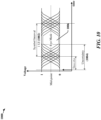
- FIG. 10 illustrates a binary eye pattern 1000 generated as an overlay of multiple symbol intervals, including a single symbol interval 1002.
- a signal transition region 1004 represents a time period of uncertainty at the boundary between two symbols where variable signal rise times prevent reliable decoding.
- State information may be determined reliably in a region defined by an eye mask 1006 within an "eye opening" that represents the time period in which the symbol is stable and can be reliably received and decoded.
- the eye mask 1006 masks off a region in which zero crossings do not occur, and the eye mask is used by the decoder to prevent multiple clocking due to the effect of subsequent zero crossings at the symbol interval boundary that follow the first signal zero crossing.
- a communication system based on Serializer/Deserializer (SERDES) technology is an example of a system where a binary eye pattern 1000 can be utilized as a basis for judging the ability to reliably recover data based on the eye opening of the binary eye pattern 1000.
- SERDES Serializer/Deserializer
- An M-wire N-Phase encoding system such as a 3-wire, 3-phase encoder may encode a signal that has at least one transition at every symbol boundary and the receiver may recover a clock using those guaranteed transitions.
- the receiver may require reliable data immediately prior to the first signal transition at a symbol boundary, and must also be able to reliably mask any occurrences of multiple transitions that are correlated to the same symbol boundary. Multiple receiver transitions may occur due to slight differences in rise and fall time between the signals carried on the M-wires (e.g. a trio of wires) and due to slight differences in signal propagation times between the combinations of signal pairs received (e.g. A-B, B-C, and C-A outputs of differential receivers 802a, 802b and 802c of FIG. 6 ).
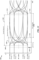
- the multi-level eye-pattern 1100 may correspond to possible transitions in 3-wire, 3-phase encoded signals provided to the differential receivers 802a, 802b, and 802c.
- the three voltage levels may cause the differential receivers 802a, 802b, and 802c to generate strong voltage levels 1126, 1128 and weak voltage levels 1122, 1124 for both positive and negative polarities.
- only one signal wire 318a, 318b and 318c is undriven in any symbol and the differential receivers 802a, 802b, and 802c do not produce a 0 state (here, 0 Volts) output.
- the voltages associated with strong and weak levels need not be evenly spaced with respect to a 0 Volts level.
- Drivers, receivers and other devices used in a C-PHY 3-Phase decoder may exhibit different switching characteristics that can introduce relative delays between signals received from the three wires. Multiple receiver output transitions may be observed at each symbol interval boundary 1108 and/or 1114 due to slight differences in the rise and fall time between the three signals of the trio of signal wires 318a, 318b, 318c and due to slight differences in signal propagation times between the combinations of pairs of signals received from the signal wires 318a, 318b, 318c.
- the multi-level eye-pattern 1100 may capture variances in rise and fall times as a relative delay in transitions near each symbol interval boundary 1108 and 1114. The variances in rise and fall times may be due to the different characteristics of the 3-Phase drivers. Differences in rise and fall times may also result in an effective shortening or lengthening of the duration of the symbol interval 1102 for any given symbol.
- the maximum speed of a communication link 220 configured for N-Phase encoding may be limited by the duration of the signal transition region 1104 compared to the eye opening 1106 corresponding to the received signal.
- the minimum period for the symbol interval 1102 may be constrained by tightened design margins associated with the CDR circuit 524 in the decoder 500 illustrated in FIG. 5 , for example.
- the programmable delay circuit 1214 may be configured in the CDR circuit 1200 to accommodate possible large variations in transition times in the difference signals 1202, 1204, 1206.
- the programmable delay circuit 1214 is typically configured to provide a minimum delay period that exceeds the duration of the timing skew between the occurrence of the first and last transitions on the difference signals 1202, 1204, 1206.
- the delay time provided by the programmable delay circuit 1214 is calculated to account for the number of logic gates in the delay loop of the CDR circuit 1200 and is constrained to a minimum delay time that accounts for expected or observed PVT variances that can affect the logic gates and/or the programmable delay circuit 1214.
- FIG. 13 is a timing diagram 1300 that illustrates certain aspects of the operation of the CDR circuit 1200.
- the diagram relates to operations after the programmable delay circuit 1214 has been configured, and the Set signal 1226 is inactive.
- the CDR circuit 1200 operates as an edge detector.
- C-PHY 3-phase encoding provides a single signaling state transition per unit interval (UI) 1302. Differences in the state of each wire of the trio, and/or transmission characteristics of the trio may cause a transition to appear at different times on two or more wires.
- the maximum difference in time of occurrence of transitions in the difference signals 1202, 1204, 1206 may be referred to as the skew time (t skew ) 1304.
- the CDR circuit 1200 may be subject to the constraint: t skew ⁇ t loop ⁇ UI .
- t loop 1320, 1406, 1506 is very sensitive to PVT.
- the data throughput obtained using a 10 GHz full-rate symbol clock signal in a conventional C-PHY interface can be obtained using a 5 GHz half-rate symbol clock signal in a C-PHY interface implemented in accordance with certain aspects of this disclosure.
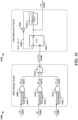
- the eg_pulse signal 1630 clocks a delay flipflop (DFF 1642) in the clock recovery circuit 1640. Each rising edge in the eg_pulse signal 1630 clocks an inverted, delayed half-rate symbol clock signal 1648 from the D input through to the output (Q) of the DFF 1642. The output of the DFF 1642 provides the half-rate symbol clock signal 1650 (rclk).
- the delay circuits 1616, 1618 and 1620 may be configured to provide pulses 1704, 1706, 1708 that have a duration sufficient to clock the DFF 1642 under expected or observed PVT conditions. For example, the duration of the pulses 1704, 1706, 1708 may be configured based on a minimum duration for a clock pulse.
- the clock recovery circuit 1640 is configured to provide a half-rate symbol clock signal 1650 that changes state at each symbol boundary 1710a, 1710b, 1710c, 1710d.
- the inverted, delayed half-rate symbol clock signal 1648 is in a logic 1 state at the first symbol boundary 1710a, while the half-rate symbol clock signal 1650 is at logic 0.
- the first rising edge in the combined pulses 1714 which corresponds to the first difference pulse 1704, clocks the logic 1 level through to the Q output of the DFF 1642, causing the half-rate symbol clock signal 1650 to transition to the logic 1 state.
- the first rising edge in the combined pulses corresponding to the second symbol boundary 1710b clocks the logic 0 level of the inverted, delayed half-rate symbol clock signal 1648 through to the Q output of the DFF 1642, causing the half-rate symbol clock signal 1650 to transition to the logic 0 state.
- the duration of a fall delay 1722 is configured to mask additional edges in the eg_pulse signal 1630 such that difference pulses corresponding to the second symbol boundary 1710b have no effect on the state of the half-rate symbol clock signal 1650.
- the delay circuit 1644 is configured to provide matching durations of the rise delay 1720 and the fall delay 1722. Configuration of the delay circuit 1644 is constrained by the need to match the durations of the rise delay 1720 and the fall delay 1722 and to mask additional pulses at symbol boundaries 1710a, 1710b, 1710c, 1710d.
- the maximum frequency of operation of the Clock recovery circuit 1640 and the corresponding minimum UI may be determined by the timing constraints associated with the clock recovery circuit 1640 and the pulse merge circuit 1600.
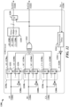
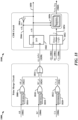
- FIG. 18 illustrates a CDR circuit 1840 that is configured to provide a high-frequency half-rate symbol clock signal 1850 from signaling transmitted through a C-PHY interface.
- Delay circuits 1816, 1818, 1820 are provided in a pulse merge circuit 1800 that generates, and merges transition pulses representative of transitions detected in the difference signals 1802, 1804, 1806.
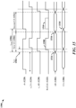
- FIG. 19 is a timing diagram 1900 that illustrates timing associated with the pulse merge circuit 1800 and the CDR circuit 1840.
- the pulse merge circuit 1800 receives difference signals 1802, 1804, 1806 that represent differences in signaling state of pairs of wires the trio of wires A, B and C.
- the difference signals 1802, 1804, 1806 are received from differential receivers or comparators such as differential receivers 802a, 802b and 802c that produce the difference signals 810a, 810b, 810c illustrated in FIG. 8 .
- the pulse merge circuit 1800 uses three exclusive-OR gates 1808, 1810, 1812 and corresponding delay circuits 1816, 1818 and 1820 to generate transition pulses 1904, 1906, 1908 in response to transitions occurring in the difference signals 1802, 1804, 1806.
- a transition in the AB difference signal 1802, the BC difference signal 1804 and the CA difference signal 1806 occurs at the each of the illustrated symbol boundaries 1910a, 1910b, 1910c, 1910d.
- the transitions in the difference signals 1802, 1804, 1806 can occur at different times, such that a timing skew 1902 can be observed between the first-occurring transition and the last-occurring transition.
- the first-occurring transition is observed at the first illustrated symbol boundary 1910a on the AB difference signal 1802 and the last-occurring transition at the first illustrated symbol boundary 1910a is observed on the CA difference signal 1806.
- the relationship between transitions can be different at each symbol boundary 1910a, 1910b, 1910c, 1910d. In operation, a transition may not occur on one of the difference signals 1802, 1804, 1806 at one or more symbol boundaries 1910a, 1910b, 1910c, 1910d.
- a first exclusive-OR gate 1808 receives the AB difference signal 1802 and a delayed version of the AB difference signal 1802 provided by the AB-delay circuit 1816, and provides an AB_p signal 1822 that includes a pulse 1904 that has a duration controlled by the duration of delay introduced by the AB-delay circuit 1816.
- a second exclusive-OR gate 1810 receives the BC difference signal 1804 and a delayed version of the BC difference signal 1804 provided by the BC-delay circuit 1818, and provides a BC_p signal 1824 that includes a pulse 1906 that has a duration controlled by the duration of delay introduced by the BC-delay circuit 1818.
- the CDR circuit 1840 is configured to provide a half-rate symbol clock signal 1850 that changes state at each symbol boundary 1910a, 1910b, 1910c, 1910d.
- the rclk_inv signal 1846 is in the logic 1 state at the first symbol boundary 1910a, while the half-rate symbol clock signal 1850 is at the logic 0 state.
- the rising edge of the combined pulse 1914 in the eg_pulse signal 1830 clocks the logic 1 level through to the Q output of the DFF 1842, causing the half-rate symbol clock signal 1850 to transition to the logic 1 state.
- the inverter 1844 generates the rclk_inv signal 1846 from the half-rate symbol clock signal 1850 with minimal delay.
- the CDR circuit 1840 includes timing circuits that may be used to delay or otherwise align the difference signals 1802, 1804, 1806 to enable capture at an edge of the half-rate symbol clock signal 1850 or a derivative of the half-rate symbol clock signal 1850.
- Aligned difference signals may be used to generate a symbol stream 1854 of three-bit raw symbols to a set of registers 1856 that are configured to capture the raw symbols from the symbol stream 1854 on both the rising edge and falling edge of the half-rate symbol clock signal 1850.
- the set of registers 1856 may include first registers that capture symbols from the symbol stream 1854 based on timing derived from rising edges in the half-rate symbol clock signal 1850 and second registers that capture symbols from the symbol stream 1854 based on timing derived from rising edges in the rclk_inv signal 1846.
- the set of registers 1856 may include one or more 3-bit shift registers and/or may be organized as a first-in, first-out (FIFO) buffer that provides a sequence of symbols 1860 that have been assembled from different registers in the set of registers 1856.
- FIFO first-in, first-out
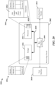
- FIG. 20 illustrates an example of a hardware implementation for an apparatus 2000 employing a processing circuit 2002 that may be configured to perform one or more functions disclosed herein.
- a processing circuit 2002 may be implemented using the processing circuit 2002.
- the processing circuit 2002 may include certain devices, circuits, and/or logic that support clock recovery techniques disclosed herein.
- the processing circuit 2002 may include one or more processors 2004 that are controlled by some combination of hardware and software modules.
- processors 2004 include microprocessors, microcontrollers, digital signal processors (DSPs), field programmable gate arrays (FPGAs), programmable logic devices (PLDs), state machines, sequencers, gated logic, discrete hardware circuits, and other suitable hardware configured to perform the various functionality described throughout this disclosure.
- DSPs digital signal processors
- FPGAs field programmable gate arrays
- PLDs programmable logic devices
- state machines sequencers, gated logic, discrete hardware circuits, and other suitable hardware configured to perform the various functionality described throughout this disclosure.
- the one or more processors 2004 may include specialized processors that perform specific functions, and that may be configured, augmented or controlled by one of the software modules 2016.
- the one or more processors 2004 may be configured through a combination of software modules 2016 loaded during initialization, and further configured by loading or unloading one or more software modules 2016 during operation.
- the processing circuit 2002 may be implemented with a bus architecture, represented generally by the bus 2010.
- the bus 2010 may include any number of interconnecting buses and bridges depending on the specific application of the processing circuit 2002 and the overall design constraints.
- the bus 2010 links together various circuits including the one or more processors 2004 and a processor-readable storage medium 2006.
- the processor-readable storage medium 2006 may include memory devices and mass storage devices, and may be referred to herein as computer-readable media and/or processor-readable media.
- the bus 2010 may also link various other circuits such as timing sources, timers, peripherals, voltage regulators, and power management circuits.
- a bus interface 2008 may provide an interface between the bus 2010 and one or more transceivers 2012.
- a transceiver 2012 may be provided for each networking technology supported by the processing circuit. In some instances, multiple networking technologies may share some or all of the circuitry or processing modules found in a transceiver 2012. Each transceiver 2012 provides a means for communicating with various other apparatus over a transmission medium. Depending upon the nature of the apparatus 2000, a user interface 2018 (e.g., keypad, display, speaker, microphone, joystick) may also be provided, and may be communicatively coupled to the bus 2010 directly or through the bus interface 2008.
- a user interface 2018 e.g., keypad, display, speaker, microphone, joystick
- Some of the software modules 2016 may be loaded during initialization of the processing circuit 2002, and these software modules 2016 may configure the processing circuit 2002 to enable performance of the various functions disclosed herein.
- some software modules 2016 may configure internal devices and/or logic circuits 2022 of the processor 2004, and may manage access to external devices such as the transceiver 2012, the bus interface 2008, the user interface 2018, timers, mathematical coprocessors, and so on.
- the software modules 2016 may include a control program and/or an operating system that interacts with interrupt handlers and device drivers, and that controls access to various resources provided by the processing circuit 2002.
- the resources may include memory, processing time, access to the transceiver 2012, the user interface 2018, and so on.
- the multitasking environment may be implemented using a timesharing program 2020 that passes control of a processor 2004 between different tasks, whereby each task returns control of the one or more processors 2004 to the timesharing program 2020 upon completion of any outstanding operations and/or in response to an input such as an interrupt.
- a task has control of the one or more processors 2004, the processing circuit is effectively specialized for the purposes addressed by the function associated with the controlling task.
- the timesharing program 2020 may include an operating system, a main loop that transfers control on a round-robin basis, a function that allocates control of the one or more processors 2004 in accordance with a prioritization of the functions, and/or an interrupt driven main loop that responds to external events by providing control of the one or more processors 2004 to a handling function.
- the receiving device may generate a transition pulse for a first difference signal by performing an exclusive OR-gate function on the first difference signal and a delayed version of the first difference signal.
- the receiving device may configure at least one pulse generating circuit to provide corresponding transition pulses with a duration based on a minimum clock pulse duration defined for the delay flipflop.
- the receiving device may calibrate at least one pulse generating circuit based on operating conditions of the three-wire bus.
- the receiving device may configure an asymmetric delay to provide a desired duration of delay applied to transitions to the first state.
- the asymmetric delay circuit is implemented as a rising-edge delay circuit configured to delay transitions from a low logic state to a high logic state.
- the rising-edge delay circuit may be further configured to pass transitions from the high logic state to the low logic state without added delay.
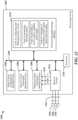
- the bus 2220 links together various circuits including one or more processors and/or hardware modules, represented by the processor 2216, the modules or circuits 2204, 2206 and 2208, difference receiver circuits 2212 that generate difference signals 2222 representative of differences in signaling state between different pairs of the connectors or wires 2214 and the processor-readable storage medium 2218.
- the bus 2220 may also link various other circuits such as timing sources, peripherals, voltage regulators, and power management circuits, which are well known in the art, and therefore, will not be described any further.
- the processor 2216 is responsible for general processing, including the execution of software stored on the processor-readable storage medium 2218.
- the software when executed by the processor 2216, causes the processing circuit 2202 to perform the various functions described supra for any particular apparatus.
- the processor-readable storage medium 2218 may also be used for storing data that is manipulated by the processor 2216 when executing software, including data decoded from symbols transmitted over the connectors or wires 2214, which may be configured as a C-PHY bus.
- the processing circuit 2202 further includes at least one of the modules 2204, 2206 and 2208.
- the modules 2204, 2206 and 2208 may be software modules running in the processor 2216, resident/stored in the processor-readable storage medium 2218, one or more hardware modules coupled to the processor 2216, or some combination thereof.
- the modules 2204, 2206 and/or 2208 may include microcontroller instructions, state machine configuration parameters, or some combination thereof.
- the apparatus 2200 may be configured for data communication in accordance with a C-PHY interface protocol.
- the apparatus 2200 may include modules and/or circuits 2208 configured to generate transition pulses responsive to transitions in signaling state of the difference signals 2222, modules and/or circuits 2206 that are configured to generate a clock signal useable to decode symbols from transitions in signaling state of the three-wire bus, and configuration modules and/or circuits 2204 for configuring delay durations used in generating the transition pulses and/or the receive clock.
- the apparatus 2200 has a plurality of pulse generating circuits, a first logic circuit and a delay flipflop.
- Each of the pulse generating circuits is configured to generate a transition pulse in response to a transition in a difference signal 2222 that is representative of a difference in signaling state of a pair of wires in a three-wire bus.
- the first logic circuit is configured to provide a single pulse in a combination signal at each boundary between pairs of sequentially-transmitted symbols by combining one or more transition pulses received from the plurality of pulse generating circuits.
- the delay flipflop responds to each pulse in the combination signal by changing signaling state of a clock signal that is output by the clock recovery apparatus.
- the symbols may be sequentially transmitted over the three-wire bus in accordance with a C-PHY protocol.
- Each pulse generating circuit may have a delay circuit configured to provide a delayed difference signal by delaying one of three difference signals, and a second logic circuit configured to provide the transition pulse by performing an exclusive OR function on the one of three difference signals and the delayed difference signal.
- the delay circuit may be configured to provide a delay that exceeds a duration of a skew between two of the three difference signals.
- the delay circuit may be configurable to provide a delay that accommodates variations in PVT conditions.
- the transition pulse may have a configurable duration.
- the delay flipflop may receive an inverse of the clock signal as its input.
- a rising edge in the clock signal can be used to capture a first symbol from the three-wire bus and a rising edge in the inverse of the clock signal can be used to capture a second symbol from the three-wire bus.
- a falling edge in the clock signal can be used to capture a first symbol from the three-wire bus and a falling edge in the inverse of the clock signal can be used to capture a second symbol from the three-wire bus.
- a rising edge in the clock signal can be used to capture a first symbol from the three-wire bus and a falling edge in the clock signal can be used to capture a second symbol from the three-wire bus.
- the processor-readable storage medium 2218 may be a non-transitory storage medium and may store instructions and/or code that, when executed a processor 2216, cause the processing circuit 2202 to generate a transition pulse in response to a transition in one of three difference signals representative of a difference in signaling state of a pair of wires in a three-wire bus, provide a single pulse in a combination signal at each boundary between pairs of sequentially-transmitted symbols by combining one or more transition pulses generated at the each boundary between the pairs of sequentially-transmitted symbols, and clock a delay flipflop with the combination signal such that signaling state of a clock signal is changed in response to each pulse in the combination signal. Transitions in one or more difference signals can occur at boundaries between symbols that are sequentially transmitted over the three-wire bus.
- the instructions may cause the processing circuit 2202 to provide a delayed difference signal by delaying one of three difference signals, and perform an exclusive OR function on the one of three difference signals and the delayed difference signal to obtain the transition pulse.
- the instructions may cause the processing circuit 2202 to delay the one of three difference signals by a duration that exceeds a duration of a skew between two of the three difference signals.
- the instructions may cause the processing circuit 2202 to delay the one of three difference signals by a duration that accommodates variations in PVT conditions.
- the transition pulse can have a configurable duration.
- the instructions may cause the processing circuit 2202 to provide an inverse of the clock signal as an input to the delay flipflop, use a rising edge in the clock signal to capture a first symbol from the three-wire bus, and use a falling edge in the clock signal to capture a second symbol from the three-wire bus.
Landscapes
- Engineering & Computer Science (AREA)
- Computer Networks & Wireless Communication (AREA)
- Signal Processing (AREA)
- Theoretical Computer Science (AREA)
- Physics & Mathematics (AREA)
- General Engineering & Computer Science (AREA)
- General Physics & Mathematics (AREA)
- Dc Digital Transmission (AREA)
- Synchronisation In Digital Transmission Systems (AREA)
Claims (15)
- Appareil de récupération d'horloge (100, 200, 2000, 2200) comprenant :trois circuits de génération d'impulsions (1608, 1610, 1612, 1808, 1810, 1812), chaque circuit de génération d'impulsions (1608, 1610, 1612, 1808, 1810, 1812) étant configuré pour générer une impulsion de transition (1408, 1704, 1706, 1708, 1904, 1906, 1908) en réponse à une transition de l'un de trois signaux de différence (810a, 1202, 1602, 1802, 2222) représentatifs d'une différence d'état de signalisation (602) d'une paire de fils dans un bus à trois fils (2010, 2220), dans lequel des transitions (1516) de l'un ou de plusieurs signaux de différence (810a, 1202, 1602, 1802, 2222) se produisent à des limites entre des symboles (514) qui sont transmis séquentiellement sur le bus à trois fils (2010, 2220) ;un premier circuit logique (1614, 1814) configuré pour fournir une impulsion unique (1714, 1914) d'un signal de combinaison (1630, 1830) à chaque limite entre des paires de symboles transmis séquentiellement (514) en combinant une ou plusieurs impulsions de transition 1408, 1704, 1706, 1708, 1904, 1906, 1908) reçues en provenance des trois circuits de génération d'impulsions (1608, 1610, 1612, 1808, 1810, 1812) ; etune bascule à retard (1642, 1842) configurée pour répondre à chaque impulsion unique (1714, 1914) du signal de combinaison en modifiant l'état de signalisation d'un signal d'horloge (1650, 1850) qui est fourni en sortie par l'appareil de récupération d'horloge (100, 200, 2000, 2200), dans lequel, pour répondre à une première impulsion unique (1714, 1914), la bascule à retard (1642, 1842) est configurée pour modifier l'état de signalisation d'un état logique 0 à un état logique 1 et, en réponse à une deuxième impulsion unique (1714, 1914), la bascule à retard (1642, 1842) est configurée pour modifier l'état de signalisation d'un état logique 1 à un état logique 0.
- Appareil de récupération d'horloge (100, 200, 2000, 2200) selon la revendication 1, dans lequel chaque circuit de génération d'impulsions (1608, 1610, 1612, 1808, 1810, 1812) comprend :un circuit de retard (712, 714, 716) configuré pour fournir un signal de différence retardé (1606, 1806, 2222) en retardant l'un des trois signaux de différence (810a, 1202, 1602, 1802, 2222) ; etun deuxième circuit logique (1608, 1610, 1612, 1808, 1810, 1812) configuré pour fournir l'impulsion de transition (1408, 1704, 1706, 1708, 1904, 1906, 1908) en exécutant une fonction OU exclusive sur l'un des trois signaux de différence (810a, 1202, 1602, 1802, 2222) et le signal de différence retardé (1606, 1806, 2222).
- Appareil de récupération d'horloge (100, 200, 2000, 2200) selon la revendication 2, dans lequel le circuit de retard (712, 714, 716) est configuré pour fournir un retard (712, 714, 716) qui dépasse une durée d'un décalage (1702) entre deux des trois signaux de différence (810a, 1202, 1602, 1802, 2222).
- Appareil de récupération d'horloge (100, 200, 2000, 2200) selon la revendication 2, dans lequel le circuit de retard (712, 714, 716) est configurable pour fournir un retard (712, 714, 716) qui s'adapte à des modifications de conditions du processus de fabrication, de tension d'alimentation du circuit et de température de la puce (PVT).
- Appareil de récupération d'horloge (100, 200, 2000, 2200) selon la revendication 4, dans lequel l'impulsion de transition (1408, 1704, 1706, 1708, 1904, 1906, 1908) a une durée configurable.
- Appareil de récupération d'horloge (100, 200, 2000, 2200) selon la revendication 1, dans lequel la bascule à retard (1642, 1842) reçoit un inverse (1648, 1846) du signal d'horloge (1650, 1850) comme entrée.
- Appareil de récupération d'horloge (100, 200, 2000, 2200) selon la revendication 6, dans lequel un front montant du signal d'horloge (1650, 1850) est utilisé pour capturer un premier symbole (702) à partir du bus à trois fils (2010, 2220) et un front montant de l'inverse du signal d'horloge (1650, 1850) est utilisé pour capturer un deuxième symbole (704) à partir du bus à trois fils (2010, 2220).
- Appareil de récupération d'horloge (100, 200, 2000, 2200) selon la revendication 6, dans lequel un front descendant du signal d'horloge (1650, 1850) est utilisé pour capturer un premier symbole (702) à partir du bus à trois fils (2010, 2220) et un front descendant de l'inverse du signal d'horloge (1650, 1850) est utilisé pour capturer un deuxième symbole (704) à partir du bus à trois fils (2010, 2220).
- Appareil de récupération d'horloge (100, 200, 2000, 2200) selon la revendication 6, dans lequel un front montant du signal d'horloge (1650, 1850) est utilisé pour capturer un premier symbole (702) à partir du bus à trois fils (2010, 2220) et un front descendant de l'inverse du signal d'horloge (1650, 1850) est utilisé pour capturer un deuxième symbole (704) à partir du bus à trois fils (2010, 2220).
- Appareil de récupération d'horloge (100, 200, 2000, 2200) selon la revendication 1, dans lequel les symboles (514) sont transmis séquentiellement sur le bus à trois fils (2010, 2220) conformément à un protocole C-PHY.
- Procédé de récupération (526) d'horloge comprenant :la génération d'une impulsion de transition (1408, 1704, 1706, 1708, 1904, 1906, 1908) en réponse à une transition de l'un de trois signaux de différence (810a, 1202, 1602, 1802, 2222) représentatifs d'une différence d'état de signalisation (602) d'une paire de fils dans un bus à trois fils (2010, 2220), dans lequel des transitions (1516) d'un ou de plusieurs signaux de différence (810a, 1202, 1602, 1802, 2222) se produisent à des limites entre des symboles (514) qui sont transmis séquentiellement sur le bus à trois fils (2010, 2220) ;la fourniture d'une impulsion unique (1714, 1914) d'un signal de combinaison (1630, 1830) à chaque limite entre des paires de symboles transmis séquentiellement (514) en combinant une ou plusieurs impulsions de transition (1408, 1704, 1706, 1708, 1904, 1906, 1908) générées au niveau de chaque limite entre les paires de symboles transmis séquentiellement (514) ; etle cadencement d'une bascule à retard (1642, 1842) avec le signal de combinaison de sorte que l'état de signalisation d'un signal d'horloge (1650, 1850) soit modifié en réponse à chaque impulsion unique (1714, 1914) du signal de combinaison, dans lequel, pour répondre à une première impulsion unique (1714, 1914), la bascule à retard (1642, 1842) est configurée pour modifier l'état de signalisation d'un état logique 0 à un état logique 1 et, en réponse à une deuxième impulsion unique (1714, 1914), la bascule à retard (1642, 1842) est configurée pour modifier l'état de signalisation d'un état logique 1 à un état logique 0.
- Procédé de récupération (526) d'horloge selon la revendication 11, dans lequel la fourniture de l'impulsion unique (1714, 1914) du signal de combinaison comprend :la fourniture d'un signal de différence retardé (1606, 1806, 2222) en retardant l'un des trois signaux de différence (810a, 1202, 1602, 1802, 2222) ; etl'exécution d'une fonction OU exclusif sur l'un des trois signaux de différence (810a, 1202, 1602, 1802, 2222) et le signal de différence retardé (1606, 1806, 2222) pour obtenir l'impulsion de transition (1408, 1704, 1706, 1708, 1904, 1906, 1908) ; de préférencecomprenant en outre :
le retard de l'un des trois signaux de différence (810a, 1202, 1602, 1802, 2222) d'un retard qui dépasse une durée d'un décalage (1702) entre deux des trois signaux de différence (810a, 1202, 1602, 1802, 2222) ; oucomprenant en outre :
le retard de l'un des trois signaux de différence (810a, 1202, 1602, 1802, 2222) d'un retard qui s'adapte à des modifications de conditions du processus de fabrication, de tension d'alimentation du circuit et de température de la puce (PVT). - Procédé de récupération (526) d'horloge selon la revendication 11, dans lequel l'impulsion de transition (1408, 1704, 1706, 1708, 1904, 1906, 1908) a une durée configurable ; ou
dans lequel les symboles (514) sont transmis séquentiellement sur le bus à trois fils (2010, 2220) conformément à un protocole C-PHY. - Procédé de récupération (526) d'horloge selon la revendication 11, comprenant en outre :la fourniture d'un inverse du signal d'horloge (1650, 1850) comme entrée de la bascule à retard (1642, 1842) ;comprenant en outre, de préférence :l'utilisation d'un front montant du signal d'horloge (1650, 1850) pour capturer un premier symbole (702) à partir du bus à trois fils (2010, 2220) ; etl'utilisation d'un front descendant du signal d'horloge (1650, 1850) pour capturer un deuxième symbole (704) à partir du bus à trois fils (2010, 2220).
- Support de stockage lisible par un processeur (2006, 2218) ayant une ou plusieurs instructions qui, lorsqu'elles sont exécutées par au moins un processeur (112, 206, 2004, 2216) d'un circuit de traitement (102, 2002) dans un récepteur, amènent l'au moins un processeur (112, 206, 2004, 2216) à :générer une impulsion de transition (1408, 1704, 1706, 1708, 1904, 1906, 1908) en réponse à une transition de l'un de trois signaux de différence (810a, 1202, 1602, 1802, 2222) représentatifs d'une différence d'état de signalisation (602) d'une paire de fils dans un bus à trois fils (2010, 2220), dans lequel des transitions (1516) d'un ou de plusieurs signaux de différence (810a, 1202, 1602, 1802, 2222) se produisent à des limites entre des symboles (514) qui sont transmis séquentiellement sur le bus à trois fils (2010, 2220) ;fournir une impulsion unique (1714, 1914) d'un signal de combinaison à chaque limite entre des paires de symboles transmis séquentiellement (514) en combinant une ou plusieurs impulsions de transition (1408, 1704, 1706, 1708, 1904, 1906, 1908) générées à chaque limite entre les paires de symboles transmis séquentiellement (514) ; etcadencer une bascule à retard (1642, 1842) avec le signal de combinaison de sorte que l'état de signalisation soit modifié en réponse à chaque impulsion unique (1714, 1914) du signal de combinaison, dans lequel, pour répondre à une première impulsion unique (1714, 1914), la bascule à retard (1642, 1842) est configurée pour modifier l'état de signalisation d'un état logique 0 à un état logique 1 et, en réponse à une deuxième impulsion unique (1714, 1914), la bascule à retard (1642, 1842) est configurée pour modifier l'état de signalisation d'un état logique 1 à un état logique 0.
Applications Claiming Priority (2)
| Application Number | Priority Date | Filing Date | Title |
|---|---|---|---|
| US16/711,230 US11038666B1 (en) | 2019-12-11 | 2019-12-11 | Open-loop, super fast, half-rate clock and data recovery for next generation C-PHY interfaces |
| PCT/US2020/057687 WO2021118700A1 (fr) | 2019-12-11 | 2020-10-28 | Récupération de données et d'horloge à demi-fréquence en boucle ouverte très rapide pour des interfaces de couches physiques (c-phy) de prochaine génération |
Publications (3)
| Publication Number | Publication Date |
|---|---|
| EP4073661A1 EP4073661A1 (fr) | 2022-10-19 |
| EP4073661C0 EP4073661C0 (fr) | 2025-04-09 |
| EP4073661B1 true EP4073661B1 (fr) | 2025-04-09 |
Family
ID=73402193
Family Applications (1)
| Application Number | Title | Priority Date | Filing Date |
|---|---|---|---|
| EP20807235.5A Active EP4073661B1 (fr) | 2019-12-11 | 2020-10-28 | Récupération de données et d'horloge à demi-fréquence en boucle ouverte très rapide pour des interfaces de couches physiques (c-phy) de prochaine génération |
Country Status (9)
| Country | Link |
|---|---|
| US (1) | US11038666B1 (fr) |
| EP (1) | EP4073661B1 (fr) |
| JP (1) | JP7358646B2 (fr) |
| KR (1) | KR102420905B1 (fr) |
| CN (1) | CN114787788B (fr) |
| BR (1) | BR112022010485A2 (fr) |
| PH (1) | PH12022551089A1 (fr) |
| TW (1) | TWI762012B (fr) |
| WO (1) | WO2021118700A1 (fr) |
Families Citing this family (5)
| Publication number | Priority date | Publication date | Assignee | Title |
|---|---|---|---|---|
| CN115001486A (zh) * | 2021-03-01 | 2022-09-02 | 中兴通讯股份有限公司 | 时钟数据恢复电路及时钟数据恢复方法 |
| US11764733B2 (en) * | 2021-09-23 | 2023-09-19 | Qualcomm Incorporated | C-PHY receiver with self-regulated common mode servo loop |
| CN116684722B (zh) * | 2023-07-27 | 2023-10-20 | 武汉精立电子技术有限公司 | Mipi c-phy信号接收装置、方法及摄像头模组测试系统 |
| KR102694980B1 (ko) | 2024-02-08 | 2024-08-14 | 주식회사 램쉽 | 신호수신회로, 신호수신장치 및 수신신호의 클럭복원방법 |
| CN121301115B (zh) * | 2025-12-11 | 2026-03-17 | 巨霖科技(上海)有限公司 | 一种mipi c-phy眼图仿真方法、计算机设备、程序产品及存储介质 |
Family Cites Families (21)
| Publication number | Priority date | Publication date | Assignee | Title |
|---|---|---|---|---|
| WO2010080172A1 (fr) * | 2009-01-12 | 2010-07-15 | Rambus Inc. | Système de signalisation de faible puissance à transfert d'horloge |
| US20140281085A1 (en) | 2013-03-15 | 2014-09-18 | Gregory L. Ebert | Method, apparatus, system for hybrid lane stalling or no-lock bus architectures |
| WO2015176244A1 (fr) * | 2014-05-21 | 2015-11-26 | Qualcomm Incorporated | Convertisseur parallèle-série et série-parallèle pour bus de données parallèles à rapport impair |
| US9548876B2 (en) * | 2015-05-06 | 2017-01-17 | Mediatek Inc. | Multiple transmitter system and method for controlling impedances of multiple transmitter system |
| KR20170008077A (ko) * | 2015-07-13 | 2017-01-23 | 에스케이하이닉스 주식회사 | 고속 통신을 위한 인터페이스 회로 및 이를 포함하는 시스템 |
| US9496879B1 (en) * | 2015-09-01 | 2016-11-15 | Qualcomm Incorporated | Multiphase clock data recovery for a 3-phase interface |
| US9485080B1 (en) * | 2015-09-01 | 2016-11-01 | Qualcomm Incorporated | Multiphase clock data recovery circuit calibration |
| US9762228B2 (en) * | 2015-09-15 | 2017-09-12 | Qualcomm Incorporated | High-speed programmable clock divider |
| US10951389B2 (en) * | 2015-11-30 | 2021-03-16 | Sony Semiconductor Solutions Corporation | Phase detector, phase synchronization circuit, and method of controlling phase synchronization circuit |
| JP6809484B2 (ja) * | 2016-01-08 | 2021-01-06 | ソニー株式会社 | 同期回路および同期回路の制御方法 |
| US10419246B2 (en) * | 2016-08-31 | 2019-09-17 | Qualcomm Incorporated | C-PHY training pattern for adaptive equalization, adaptive edge tracking and delay calibration |
| US9735950B1 (en) * | 2016-10-18 | 2017-08-15 | Omnivision Technologies, Inc. | Burst mode clock data recovery circuit for MIPI C-PHY receivers |
| AU2017350752A1 (en) * | 2016-10-24 | 2019-03-28 | Qualcomm Incorporated | Reducing transmitter encoding jitter in a C-PHY interface using multiple clock phases to launch symbols |
| US10033519B2 (en) * | 2016-11-10 | 2018-07-24 | Qualcomm Incorporated | C-PHY half-rate clock and data recovery adaptive edge tracking |
| KR102784755B1 (ko) * | 2016-11-29 | 2025-03-24 | 삼성전자주식회사 | 통신 환경에 의존하여 지연을 조절하는 전자 회로 |
| KR102629185B1 (ko) * | 2016-12-07 | 2024-01-24 | 에스케이하이닉스 주식회사 | 데이터 통신을 위한 수신기 |
| CN118117305A (zh) * | 2016-12-21 | 2024-05-31 | 英特尔公司 | 无线通信技术、装置和方法 |
| US10630295B2 (en) | 2018-04-23 | 2020-04-21 | Synaptics Incorporated | Device and method for detecting signal state transition |
| US10298381B1 (en) * | 2018-04-30 | 2019-05-21 | Qualcomm Incorporated | Multiphase clock data recovery with adaptive tracking for a multi-wire, multi-phase interface |
| US10333690B1 (en) * | 2018-05-04 | 2019-06-25 | Qualcomm Incorporated | Calibration pattern and duty-cycle distortion correction for clock data recovery in a multi-wire, multi-phase interface |
| US10263766B1 (en) | 2018-06-11 | 2019-04-16 | Qualcomm Incorporated | Independent pair 3-phase eye sampling circuit |
-
2019
- 2019-12-11 US US16/711,230 patent/US11038666B1/en active Active
-
2020
- 2020-10-28 BR BR112022010485A patent/BR112022010485A2/pt unknown
- 2020-10-28 JP JP2022534796A patent/JP7358646B2/ja active Active
- 2020-10-28 WO PCT/US2020/057687 patent/WO2021118700A1/fr not_active Ceased
- 2020-10-28 KR KR1020227018549A patent/KR102420905B1/ko active Active
- 2020-10-28 EP EP20807235.5A patent/EP4073661B1/fr active Active
- 2020-10-28 PH PH1/2022/551089A patent/PH12022551089A1/en unknown
- 2020-10-28 CN CN202080086353.1A patent/CN114787788B/zh active Active
- 2020-11-04 TW TW109138360A patent/TWI762012B/zh active
Also Published As
| Publication number | Publication date |
|---|---|
| CN114787788A (zh) | 2022-07-22 |
| US20210184829A1 (en) | 2021-06-17 |
| JP7358646B2 (ja) | 2023-10-10 |
| EP4073661C0 (fr) | 2025-04-09 |
| TWI762012B (zh) | 2022-04-21 |
| KR20220083842A (ko) | 2022-06-20 |
| KR102420905B1 (ko) | 2022-07-13 |
| TW202133559A (zh) | 2021-09-01 |
| CN114787788B (zh) | 2024-08-20 |
| PH12022551089A1 (en) | 2023-09-18 |
| WO2021118700A1 (fr) | 2021-06-17 |
| EP4073661A1 (fr) | 2022-10-19 |
| JP2022552022A (ja) | 2022-12-14 |
| BR112022010485A2 (pt) | 2022-09-06 |
| US11038666B1 (en) | 2021-06-15 |
Similar Documents
| Publication | Publication Date | Title |
|---|---|---|
| EP3345333B1 (fr) | Étalonnage de circuit de récupération de données d'horloge multiphase | |
| CA2992751C (fr) | Recuperation de donnees d'horloge multi-phase pour une interface triphasee | |
| US10033519B2 (en) | C-PHY half-rate clock and data recovery adaptive edge tracking | |
| US10419246B2 (en) | C-PHY training pattern for adaptive equalization, adaptive edge tracking and delay calibration | |
| EP4049402B1 (fr) | Horloge à retard de petite boucle et bloc de récupération de données pour un c-phy de prochaine génération à grande vitesse | |
| US9553635B1 (en) | Time based equalization for a C-PHY 3-phase transmitter | |
| EP4073661B1 (fr) | Récupération de données et d'horloge à demi-fréquence en boucle ouverte très rapide pour des interfaces de couches physiques (c-phy) de prochaine génération | |
| US10298381B1 (en) | Multiphase clock data recovery with adaptive tracking for a multi-wire, multi-phase interface | |
| US11463233B2 (en) | Unit interval jitter improvement in a C-PHY interface | |
| US11327914B1 (en) | C-PHY data-triggered edge generation with intrinsic half-rate operation | |
| US10263766B1 (en) | Independent pair 3-phase eye sampling circuit |
Legal Events
| Date | Code | Title | Description |
|---|---|---|---|
| STAA | Information on the status of an ep patent application or granted ep patent |
Free format text: STATUS: UNKNOWN |
|
| STAA | Information on the status of an ep patent application or granted ep patent |
Free format text: STATUS: THE INTERNATIONAL PUBLICATION HAS BEEN MADE |
|
| PUAI | Public reference made under article 153(3) epc to a published international application that has entered the european phase |
Free format text: ORIGINAL CODE: 0009012 |
|
| STAA | Information on the status of an ep patent application or granted ep patent |
Free format text: STATUS: REQUEST FOR EXAMINATION WAS MADE |
|
| 17P | Request for examination filed |
Effective date: 20220506 |
|
| AK | Designated contracting states |
Kind code of ref document: A1 Designated state(s): AL AT BE BG CH CY CZ DE DK EE ES FI FR GB GR HR HU IE IS IT LI LT LU LV MC MK MT NL NO PL PT RO RS SE SI SK SM TR |
|
| DAV | Request for validation of the european patent (deleted) | ||
| DAX | Request for extension of the european patent (deleted) | ||
| STAA | Information on the status of an ep patent application or granted ep patent |
Free format text: STATUS: EXAMINATION IS IN PROGRESS |
|
| 17Q | First examination report despatched |
Effective date: 20231130 |
|
| GRAP | Despatch of communication of intention to grant a patent |
Free format text: ORIGINAL CODE: EPIDOSNIGR1 |
|
| STAA | Information on the status of an ep patent application or granted ep patent |
Free format text: STATUS: GRANT OF PATENT IS INTENDED |
|
| INTG | Intention to grant announced |
Effective date: 20241105 |
|
| GRAS | Grant fee paid |
Free format text: ORIGINAL CODE: EPIDOSNIGR3 |
|
| GRAA | (expected) grant |
Free format text: ORIGINAL CODE: 0009210 |
|
| STAA | Information on the status of an ep patent application or granted ep patent |
Free format text: STATUS: THE PATENT HAS BEEN GRANTED |
|
| AK | Designated contracting states |
Kind code of ref document: B1 Designated state(s): AL AT BE BG CH CY CZ DE DK EE ES FI FR GB GR HR HU IE IS IT LI LT LU LV MC MK MT NL NO PL PT RO RS SE SI SK SM TR |
|
| REG | Reference to a national code |
Ref country code: GB Ref legal event code: FG4D |
|
| REG | Reference to a national code |
Ref country code: CH Ref legal event code: EP |
|
| REG | Reference to a national code |
Ref country code: DE Ref legal event code: R096 Ref document number: 602020049199 Country of ref document: DE |
|
| REG | Reference to a national code |
Ref country code: IE Ref legal event code: FG4D |
|
| U01 | Request for unitary effect filed |
Effective date: 20250430 |
|
| U07 | Unitary effect registered |
Designated state(s): AT BE BG DE DK EE FI FR IT LT LU LV MT NL PT RO SE SI Effective date: 20250512 |
|
| PG25 | Lapsed in a contracting state [announced via postgrant information from national office to epo] |
Ref country code: ES Free format text: LAPSE BECAUSE OF FAILURE TO SUBMIT A TRANSLATION OF THE DESCRIPTION OR TO PAY THE FEE WITHIN THE PRESCRIBED TIME-LIMIT Effective date: 20250409 |
|
| PG25 | Lapsed in a contracting state [announced via postgrant information from national office to epo] |
Ref country code: NO Free format text: LAPSE BECAUSE OF FAILURE TO SUBMIT A TRANSLATION OF THE DESCRIPTION OR TO PAY THE FEE WITHIN THE PRESCRIBED TIME-LIMIT Effective date: 20250709 Ref country code: GR Free format text: LAPSE BECAUSE OF FAILURE TO SUBMIT A TRANSLATION OF THE DESCRIPTION OR TO PAY THE FEE WITHIN THE PRESCRIBED TIME-LIMIT Effective date: 20250710 |
|
| PG25 | Lapsed in a contracting state [announced via postgrant information from national office to epo] |
Ref country code: PL Free format text: LAPSE BECAUSE OF FAILURE TO SUBMIT A TRANSLATION OF THE DESCRIPTION OR TO PAY THE FEE WITHIN THE PRESCRIBED TIME-LIMIT Effective date: 20250409 |
|
| PGFP | Annual fee paid to national office [announced via postgrant information from national office to epo] |
Ref country code: GB Payment date: 20250911 Year of fee payment: 6 |
|
| PG25 | Lapsed in a contracting state [announced via postgrant information from national office to epo] |
Ref country code: HR Free format text: LAPSE BECAUSE OF FAILURE TO SUBMIT A TRANSLATION OF THE DESCRIPTION OR TO PAY THE FEE WITHIN THE PRESCRIBED TIME-LIMIT Effective date: 20250409 |
|
| PG25 | Lapsed in a contracting state [announced via postgrant information from national office to epo] |
Ref country code: RS Free format text: LAPSE BECAUSE OF FAILURE TO SUBMIT A TRANSLATION OF THE DESCRIPTION OR TO PAY THE FEE WITHIN THE PRESCRIBED TIME-LIMIT Effective date: 20250709 |
|
| PGFP | Annual fee paid to national office [announced via postgrant information from national office to epo] |
Ref country code: IE Payment date: 20250912 Year of fee payment: 6 |
|
| U20 | Renewal fee for the european patent with unitary effect paid |
Year of fee payment: 6 Effective date: 20250915 |
|
| PG25 | Lapsed in a contracting state [announced via postgrant information from national office to epo] |
Ref country code: IS Free format text: LAPSE BECAUSE OF FAILURE TO SUBMIT A TRANSLATION OF THE DESCRIPTION OR TO PAY THE FEE WITHIN THE PRESCRIBED TIME-LIMIT Effective date: 20250809 |
|
| PG25 | Lapsed in a contracting state [announced via postgrant information from national office to epo] |
Ref country code: SM Free format text: LAPSE BECAUSE OF FAILURE TO SUBMIT A TRANSLATION OF THE DESCRIPTION OR TO PAY THE FEE WITHIN THE PRESCRIBED TIME-LIMIT Effective date: 20250409 |
|
| PG25 | Lapsed in a contracting state [announced via postgrant information from national office to epo] |
Ref country code: CZ Free format text: LAPSE BECAUSE OF FAILURE TO SUBMIT A TRANSLATION OF THE DESCRIPTION OR TO PAY THE FEE WITHIN THE PRESCRIBED TIME-LIMIT Effective date: 20250409 |
|
| PG25 | Lapsed in a contracting state [announced via postgrant information from national office to epo] |
Ref country code: SK Free format text: LAPSE BECAUSE OF FAILURE TO SUBMIT A TRANSLATION OF THE DESCRIPTION OR TO PAY THE FEE WITHIN THE PRESCRIBED TIME-LIMIT Effective date: 20250409 |
|
| PLBE | No opposition filed within time limit |
Free format text: ORIGINAL CODE: 0009261 |
|
| STAA | Information on the status of an ep patent application or granted ep patent |
Free format text: STATUS: NO OPPOSITION FILED WITHIN TIME LIMIT |
|
| REG | Reference to a national code |
Ref country code: CH Ref legal event code: L10 Free format text: ST27 STATUS EVENT CODE: U-0-0-L10-L00 (AS PROVIDED BY THE NATIONAL OFFICE) Effective date: 20260218 |
|
| 26N | No opposition filed |
Effective date: 20260112 |