EP4073882B1 - Dissipateur thermique intégré et structure d'antenne - Google Patents
Dissipateur thermique intégré et structure d'antenne Download PDFInfo
- Publication number
- EP4073882B1 EP4073882B1 EP20829134.4A EP20829134A EP4073882B1 EP 4073882 B1 EP4073882 B1 EP 4073882B1 EP 20829134 A EP20829134 A EP 20829134A EP 4073882 B1 EP4073882 B1 EP 4073882B1
- Authority
- EP
- European Patent Office
- Prior art keywords
- heatsink
- radio frequency
- frequency antenna
- antenna
- integrated
- Prior art date
- Legal status (The legal status is an assumption and is not a legal conclusion. Google has not performed a legal analysis and makes no representation as to the accuracy of the status listed.)
- Active
Links
Images





Classifications
-
- H—ELECTRICITY
- H01—ELECTRIC ELEMENTS
- H01Q—ANTENNAS, i.e. RADIO AERIALS
- H01Q1/00—Details of, or arrangements associated with, antennas
- H01Q1/12—Supports; Mounting means
- H01Q1/22—Supports; Mounting means by structural association with other equipment or articles
- H01Q1/24—Supports; Mounting means by structural association with other equipment or articles with receiving set
- H01Q1/241—Supports; Mounting means by structural association with other equipment or articles with receiving set used in mobile communications, e.g. GSM
- H01Q1/246—Supports; Mounting means by structural association with other equipment or articles with receiving set used in mobile communications, e.g. GSM specially adapted for base stations
-
- H—ELECTRICITY
- H01—ELECTRIC ELEMENTS
- H01Q—ANTENNAS, i.e. RADIO AERIALS
- H01Q1/00—Details of, or arrangements associated with, antennas
- H01Q1/02—Arrangements for de-icing; Arrangements for drying-out ; Arrangements for cooling; Arrangements for preventing corrosion
-
- H—ELECTRICITY
- H01—ELECTRIC ELEMENTS
- H01Q—ANTENNAS, i.e. RADIO AERIALS
- H01Q1/00—Details of, or arrangements associated with, antennas
- H01Q1/44—Details of, or arrangements associated with, antennas using equipment having another main function to serve additionally as an antenna, e.g. means for giving an antenna an aesthetic aspect
-
- H—ELECTRICITY
- H01—ELECTRIC ELEMENTS
- H01Q—ANTENNAS, i.e. RADIO AERIALS
- H01Q9/00—Electrically-short antennas having dimensions not more than twice the operating wavelength and consisting of conductive active radiating elements
- H01Q9/04—Resonant antennas
- H01Q9/0407—Substantially flat resonant element parallel to ground plane, e.g. patch antenna
- H01Q9/0421—Substantially flat resonant element parallel to ground plane, e.g. patch antenna with a shorting wall or a shorting pin at one end of the element
Definitions
- Wireless communication technologies have been growing in popularity and use over the past several years. This growth has been fueled by better communications hardware, larger networks, and more reliable protocols. Wireless and Internet service providers are now able to offer their customers with an ever-expanding array of features and services, such as robust cloud-based services.
- edge devices e.g., routers, switches, etc.
- SoCs system-on-chips
- memories e.g., RAM, ROM, etc.
- antennas e.g., antennas, etc.
- power amplifiers e.g., power rails, etc.
- edge devices As more functions and capabilities are added to edge devices, the amount of power consumed and dissipated by the devices increases. Power dissipation becomes more acute when the device is reduced in physical size, which reduces the horizontal and vertical surface area that is available for dissipating thermal energy or heat. Further, many edge devices are deployed or used in environments that prevent the use of (or reduce the effectiveness of) thermal management solutions that require forced airflow (e.g., via a fan, etc.) or cold intake air.
- forced airflow e.g., via a fan, etc.
- high performance edge devices which generate a significant amount of heat, are often shaped to dissipate heat (e.g., are shaped as a quadrilateral cuboid having two elongated faces/sides, etc.) and/or include large casings that house large heat sinks.
- purchasers and users of consumer facing edge devices increasingly demand that their device comply with certain size and/or physical design requirements. That is, in addition to high performance and functionality, consumers increasingly demand that their devices have an attractive form factor and a small size that allows the device to be readily placed throughout a home or small office.
- US 2018/342784 A1 , WO 2010/148019 A2 , US 2013/222201 A1 and US 2018/219277 describe known antennas coupled to heatsink arrangements.
- components and circuitry within a computing device generate heat or thermal energy, which at excessive levels could have a significant negative impact on the performance and functioning of the computing device.
- the amount of thermal energy that is generated may depend upon the components included in the computing device, operating conditions, and/or the operations or activities in the computing device.
- a computing device that wirelessly transmits data for a sustained time period at a high power-level may require that a power amplifier feed the antenna.
- the power amplifier may generate a significant amount of thermal energy that could have a negative impact on the performance of the computing device.
- processors and other components in the computing device generate a significant amount thermal energy when the performing complex tasks, such as video processing, cryptography, or machine learning.
- the thermal energy generated by these processors/components could have a significant negative impact on the performance and functioning of the computing device.
- Modern computing systems are equipped with heat dissipating structures that help ensure the device does not operate at unsafe temperatures that damage or shorten the operating life of the device.
- Modern computing systems are often also equipped with radiating structures (antennas) for sending and receiving wireless communications.
- the heat dissipating structures are separate and independent of radiating structures, and thus compete with one another for product volume (e.g., space with in the device).
- product volume e.g., space with in the device.
- device manufacturers have had to either build devices that are large enough to include both the heat dissipating and radiating structures (e.g., personal computers, laptops, routers, etc.) or build smaller but less powerful devices (e.g., smartphones, IoT devices, etc.) that attempt to balance tradeoffs between performance and power consumption.
- Device manufacturers that opt to build the small and mid-sized devices often carve away sections of the heat dissipating structure (heatsinks) to make room for the radiating structures (antennas), or vice versa.
- the tradeoff or reduction in heat dissipation structure size for antenna installation reduces the thermal performance of the device because it decreases the surface area of the heat dissipating structure. This also degrades the radiation patterns on the radiating structures and may otherwise have a negative impact on the device's performance or reliability.
- the various embodiments include an integrated heatsink and antenna structure that is suitable for inclusion in small and midsized computing devices and which overcomes the above-described limitations of conventional solutions.
- the integrated heatsink and antenna structure includes heatsink portions and radio frequency antenna portions.
- the heatsink portions provide a path for dissipating thermal energy or heat generated by the components in the device (e.g., printed circuit boards, processors, voltage amplifiers, etc.), and the radio frequency (RF) antenna portions allow the device to send and receive wireless communications.
- RF radio frequency
- the integrated heatsink and antenna structure are formed so that radio frequency antenna portions operate to improve the thermal performance of the heatsink portions and/or so that the heatsink portions operate to improve the antenna properties (e.g., radiation patterns, radiation efficiency, bandwidth, input impedance, polarization, directivity, gain, beam-width, voltage standing wave ratio, etc.) of the radio frequency antenna portions.
- antenna properties e.g., radiation patterns, radiation efficiency, bandwidth, input impedance, polarization, directivity, gain, beam-width, voltage standing wave ratio, etc.
- the various embodiments may include, use, incorporate, implement, provide access to a variety of wired and wireless communication networks, technologies and standards that are currently available or contemplated in the future, including any or all of Bluetooth ® , Bluetooth Low Energy, ZigBee, LoRa, Wireless HART, Weightless P, DASH7, RPMA, RFID, NFC, LwM2M, Adaptive Network Topology (ANT), Worldwide Interoperability for Microwave Access (WiMAX), WIFI, WiFi6,WIFI Protected Access I & II (WPA, WPA2), personal area networks (PAN), local area networks (LAN), metropolitan area networks (MAN), wide area networks (WAN), networks that implement the data over cable service interface specification (DOCSIS), networks that utilize asymmetric digital subscriber line (ADSL) technologies, third generation partnership project (3GPP), long term evolution (LTE) systems, LTE-Direct, third generation wireless mobile communication technology (3G), fourth generation wireless mobile communication technology (4G), fifth generation wireless mobile communication technology (5G), global system for mobile communications (GSM), universal mobile
- computing device may be used herein to refer to any one or all of quantum computing devices, edge devices, Internet access gateways, modems, routers, network switches, residential gateways, access points, integrated access devices (IAD), mobile convergence products, networking adapters, multiplexers, personal computers, laptop computers, tablet computers, user equipment (UE), smartphones, personal or mobile multi-media players, personal data assistants (PDAs), palm-top computers, wireless electronic mail receivers, multimedia Internet enabled cellular telephones, gaming systems (e.g., PlayStation TM , Xbox TM , Nintendo Switch TM , etc.), wearable devices (e.g., smartwatch, head-mounted display, fitness tracker, etc.), IoT devices (e.g., smart televisions, smart speakers, smart locks, lighting systems, smart switches, smart plugs, smart doorbells, smart doorbell cameras, smart air pollution/quality monitors, smart smoke alarms, security systems, smart thermostats, etc.), media players (e.g., DVD players, ROKU TM , Apple TV
- quantum computing device may be used herein to refer to a computing device or edge device, whether it is a standalone device or used in conjunction with current computing processes, that generates or manipulates quantum bits (qubits) or which utilizes quantum memory states.
- a quantum computing device may enhance edge computing capability by providing solutions that would be challenging to implement via conventional computing systems. This is especially true with value added computing for leveraging a diverse amount of senor and other input data to arrive at a solution in real time. Through unifying diverse data sources a quantum computing solution at the edge may accelerate machine learning, solve complex problems faster as well as provide the fundamental platform for artificial intelligence nodes at the edge of the network. With the vast array of data delivered by sensors as well state information the quantum computing process may improve the memory allocation though the use of superposition allowing for more information to be simultaneously stored and processed.
- edge device may be used herein to refer to a computing device that includes a programmable processor and communications circuitry for establishing communication links to consumer devices (e.g., smartphones, UEs, IoT devices, etc.) and/or to network components in a service provider, core, cloud, or enterprise network.
- consumer devices e.g., smartphones, UEs, IoT devices, etc.
- an edge device may include or implement functionality associated any one or all of an access point, gateway, modem, router, network switch, residential gateway, mobile convergence product, networking adapter, customer premise device, multiplexer and/or other similar devices.
- components and circuitry within a computing device generate heat or thermal energy, which at excessive levels may damage or reduce the performance of the computing device.
- the amount of thermal energy that is generated may vary depending upon the components included in the computing device, operating conditions, and/or the operations or activities in the computing device.
- a computing device that wirelessly transmits data for a sustained time period at a high power-level may require that a power amplifier feed its antennas.
- the power amplifier may generate a significant amount of thermal energy that could have a negative impact on the performance of the computing device.
- processors and other components in the computing device generate a significant amount thermal energy when the performing complex tasks, such as processing video, using cryptographic technology, or implementing machine learning. The thermal energy generated by these processors/components could damage the device, shorten the operating life of the device, cause the device to abruptly shut down, or otherwise have a negative impact on the device's reliability or performance characteristics.
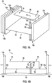
- FIGS. 1A and 1B illustrate an integrated heatsink and antenna structure 100 in accordance with the embodiments.
- the integrated heatsink and antenna structure 100 includes a radio frequency (RF) antenna portion 120 for sending and receiving wireless communications and heatsink portions 140a, 140b configured to dissipate thermal energy or heat.
- RF antenna portion 120 operates to improve the thermal performance of one or more of the heatsink portions 140a, 140b.
- the RF antenna portion 120 may be (or may be plated with) aluminum, copper, stainless steel, beryllium copper, phosphor bronze or any other similar material or composition.
- the heatsink portions 140a, 140b may be (or may be plated with) aluminum, copper, or any other material or composition suitable for dissipating heat.
- the RF antenna portion 120 may be copper and the heatsink portions 140a, 140b may be aluminum.
- the RF antenna portion 120 are formed as a planar inverted-F antenna.
- the RF antenna portion 120 may include a feed component 102, a ground plane component 104, and a radiating component 106.
- the radiating component 106 may have an L-shape, such that one leg of the L extends substantially parallel to and is offset from the ground plane component 104, while a second leg of the L (e.g., formed after a bend in the radiating component 106) extends substantially perpendicular to the first leg toward the ground plane component 104.
- one end of the second leg may be attached to or integrally formed with the ground plane component 104 at the grounded end 109.
- a monopole could be designed with the heat sink as ground reference.
- some embodiments may include a ground plane independent primary radiator (e.g. dipole, etc.) that uses the heatsink as a field shaping structure (dish on a dish antenna).
- the feed component 102 may be electrically coupled to a computing device (not illustrated), in which the integrated heatsink and antenna structure 100 is included. Also, the feed component 102 may be fixedly secured (e.g., soldered) to the radiating component 106 at a feed point 112. In this way, the feed component 102 extends from the feed point 112, through an aperture 105 in the ground plane component 104, and to a physical connection with the computing device.
- the feed component 102 may include a casing or sheathing 105 that insolates the feed component 102.
- the feed point 112 may be disposed between a shorted portion 108 and a radiating portion 110 of the radiating component 106.
- the shorted portion 108 may extend away from the feed point 112, substantially parallel to the ground plane component 104 until the bend, beyond which the remainder of the shorted portion 108 extends toward the ground plane component 104 such that the grounded end 109 ends in contact with the ground plane component 104. In this way, the shorted portion 108 may be configured to electrically short one end of the radiating component 106 to the ground plane component 104.
- the radiating portion 110 may extend away from the feed point 112, in the opposite direction from the shorted portion 108, extending substantially parallel to the ground plane component 104, but include a remote end that is not attached to any other component or portion of the integrated heatsink and antenna structure 100.
- the heatsink portions 140a, 140b each include fin components 114a, 114b that provide thermal resistance and additional surface area for improved thermal performance.
- the first fin of heatsink portion 140b may provide capacitive tuning to the open end of the 2.4 GHz patches. This may allow the patches to be smaller that would be the case without the fin.
- the fin components 114a, 114b may be (or may be plated with) aluminum, copper, or any other material or composition suitable for dissipating heat.
- the fin components 114a, 114b may be formed of a material suitable for also enhancing one or more antenna properties (e.g., radiation patterns, radiation efficiency, bandwidth, input impedance, polarization, directivity, gain, beam-width, voltage standing wave ratio, etc.) of the RF antenna portion 120.
- a greater or fewer number of fin components 114a, 114b may be included as part of the heatsink portions 140a, 140b (i.e., illustrated as ellipses on the outer right and left sides of FIG. 1B ).
- the ground plane component 104 is coupled to one or more of the fin components 114a, 114b and arranged to dissipate additional thermal energy and further improve thermal performance, similar to the fin components 114a, 114b.
- An innermost one of each of the fin components 114a, 114b include tabs 141a, 141b that hold the ground plane component 104 in place. Additional components may bias the ground plane component 104 into contact with the tabs 141a, 141b, thus securing (i.e., holding) the RF antenna portion 120 and the heatsink portions 140a, 140b together.
- a clip or slot may be provided on or in the innermost ones of the fin components 114a, 114b for securing the ground plane component 104 to the fin components 114a, 114b.
- securing the ground plane component 104 to the fin components 114a, 114b couples the RF antenna portion 120 to the heatsink portions 140a, 140b.
- this coupling produces a synergistic effect of providing an RF antenna portion 120 that improves the thermal performance of the heatsink portions 140a, 140b, as well as heatsink portions 140a, 140b that improve the antenna properties of the RF antenna portion 120.
- the computing device in which the integrated heatsink and antenna structure 100 is included, may dissipate the same amount of heat and/or achieve the same thermal performance as conventional devices that have larger structures that include larger or a greater number of fin components that occupy more area.
- the integrated heatsink and antenna structure 100 may be packaged into a smaller or more compact container and/or to include additional or more powerful components (e.g., additional antennas, more powerful processors that generate more heat, etc.) than conventional devices.
- FIGS. 2A-2C illustrate an integrated heatsink and antenna structure 200 that includes multiple sets of the integrated heatsink and antenna structure 100 described above with regard to FIG. 1 , in accordance with some embodiments.
- the integrated heatsink and antenna 200 may include numerous antennas.
- the integrated heatsink and antenna structure 200 includes eight (8) RF antenna portions 120a-h coupled to a heatsink base 210.
- the heatsink base 210 may improve the omnidirectional pattern of the antenna portions (120a-h).
- Each of the RF antenna portions 120a-h is coupled to and surrounded by fin components (e.g., 114a-d) integrated into the heatsink base 210 and that dissipate thermal energy.
- fin components e.g., 114a-d
- four (4) of the RF antenna portions 120a, 120c, 120e, 120g may be disposed on the sides of the integrated heatsink and antenna structure 200, each having a similar configuration to that described with regard to integrated heatsink and antenna structure 100 in FIGS. 1A and 1B .
- RF antenna portions 120b, 120d, 120f, 120h may be disposed on the corners of the integrated heatsink and antenna structure 200, each flanked by sets of fin components (e.g., 114b, 114c), but those flanking fin components may be disposed on two different sides of the integrated heatsink and antenna structure 200.
- the integrated heatsink and antenna structure 200 may include a cavity onto which a processor, computing system, printed circuit board, integrated circuit (IC) chips, a system on chip (SOC), or system in a package (SIP) and/or other similar components may be implemented or placed.
- the integrated heatsink and antenna structure 200 may include a connector port 202 that provides an interface between components of the integrated heatsink and antenna structure 200 and other computers or peripheral devices.
- the components/chips may be placed on a heat conducting material (not illustrated separately in FIGs. 2A-C ) that is placed on top of the cavity (or aluminum housing) to help with the heat transfer and to address any imperfections that arise during manufacturing.
- the integrated heatsink and antenna structure 200 may dissipate between approximately 15 to 20 Watts/mm 2 (or Watts/inch 2 ) from the chip to the integrated heatsink and antenna structure 200, from the integrated heatsink and antenna structure 200 to ambient air, and/or from the chip to ambient air.
- the integrated heatsink and antenna structure 200 may include multiple RF antennas 120a-h.
- the RF antennas 120a-h may include wideband, multiband, and/or ultrawideband (UWB) antennas.
- the RF antennas 120a-h may include patch antennas, inverted-L antennas, inverted-F antennas (e.g., planar inverted-F antenna (PIFA), dual frequency PIFA, etc.) or any other antenna suitable for wireless applications.
- the RF antennas 120a-h and/or the antenna pattern may be selected based on heatsink characteristics (size, area, amount of heat metal, etc.).
- ground plane component 104 couples the RF antenna portions 120 to the heatsink portion.
- the ground plane for any of the RF antenna portions 120 may be changed so that it is potentially smaller than shown in the figures, but running the entire length behind the heatsink fin components 114.
- the fin components 114 may be arraigned into a fin structure that is slightly different for each RF antenna portion 120a-h or for each antenna location.
- each of the RF antenna portions 120 may be tuned for frequency band and/or modified based on frequency, bandwidth, impedance, proximity to the fin components 114 and/or the corresponding fin structure.
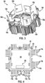
- FIG. 3 illustrates a partially exploded view of the integrated heatsink and antenna structure 200.
- the RF antenna portions 120a-h may be separated from and/or attached to the heatsink base component 210 using securing structures incorporated into some of the fin components.
- the antenna elements/portions may be formed curved of a springy material.
- the heat sink features may hold the antenna elements/portions flat so that friction (primarily) holds them in place.
- the RF antenna portions 120a-h may be attached to the heatsink base component 210 via a friction fit.
- the integrated heatsink and antenna structure 200 may be formed to fit into a plastic housing (not illustrated separately in FIG. 3 ) that has features that ensure location of the radiating element so that the antennas do not become detuned by having the structure bent out of shape.
- FIG. 4 illustrates the heatsink base component 210 in accordance with various embodiments.
- FIG. 4 shows some of the retaining structures that may be incorporated into some of the fin components for holding and retaining the RF antenna portions (e.g., 120a-h).
- the corner fin components may have hooked ends 441 such that the hooked ends 441 on a pair of opposed corner fin components may bend toward one another.
- the hooked ends 441 may be used to secure or trap an RF antenna portion (or components thereof).
- the RF antenna portion may also be supported by corner mini-fins 451 that project out toward the RF antenna portion.
- each of the RF antenna portions on the corners of the heatsink base component 210 may be trapped between a pair of the hooked ends 441 and a set of the corner mini-fins 451.
- the RF antenna portions on the sides of the heatsink base component 210 may be trapped between a pair of the tabs 141a, 141b and a set of additional mini-fins 453.
- FIGS. 5A and 5B illustrate a stackable housing 500 for an integrated heatsink and antenna structure in accordance with various embodiments.
- the stackable housing 500 may include a lid 510, an upper rim 520, an upper tray 530, a housing casing 540, housing base 550, and housing feet 555.
- the integrated heatsink and antenna structure e.g., 200
- the housing casing 540 may be slipped over and surround the integrated heatsink and antenna structure 200.
- the lid 510, upper rim 520, and upper tray 530 may then close off the assembly by being secured on top of the housing casing 540. Additional components and/or circuitry may be located between the integrated heatsink and antenna structure and the housing base 550.
- components and/or circuitry may be located between the lid 510 and the upper tray 530.
- the stackable housing 500 may be stacked on top of or below another stackable housing 500, which then allows multiple integrated heatsink and antenna structures (e.g., 200) to be used together in a compact arrangement.
- the lid 510, upper rim 520, and upper tray 530 of all but the uppermost stackable housing 500 are removed, which may expose one integrated heatsink and antenna structure below to another integrated heatsink and antenna structure above.
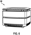
- FIG. 6 illustrates two of the stackable housings shown in FIGS 5A and 5B stacked on top of and couple to one another in accordance with various embodiments.
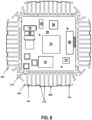
- FIG. 7 illustrates an example computing system 700 that may be used with integrated heatsink and antenna structure 200 in accordance with some embodiments.
- the computing system 700 includes an SOC 702, a clock 704, and a voltage regulator 706.
- an SOC may be a single IC chip that contains multiple resources and/or processors integrated on a single substrate.
- a single SOC may contain circuitry for digital, analog, mixed-signal, and radio-frequency functions.
- a single SOC may also include any number of general purpose and/or specialized processors (packet processors, etc.), memory blocks (e.g., ROM, RAM, Flash, etc.), and resources (e.g., timers, voltage regulators, oscillators, etc.).
- SOCs may also include software for controlling the integrated resources and processors, as well as for controlling peripheral devices.
- the components in an SOC may generate a significant amount of thermal energy or heat, and thus the placement of the components within the SOC, the location of the SOC within the integrated heatsink and antenna structure 200, and other thermal management considerations are often important.
- the SOC 702 may include a digital signal processor (DSP) 708, a modem processor 710, a graphics processor 712, an application processor 714 connected to one or more of the processors, memory 716, custom circuitry 718, system components and resources 720, a thermal management unit 722, and an interconnection/bus module 724.
- DSP digital signal processor
- the SOC 702 may operate as central processing unit (CPU) that carries out the instructions of software application programs by performing the arithmetic, logical, control and input/output (I/O) operations specified by the instructions.
- CPU central processing unit
- the thermal management unit 722 may be configured to monitor and manage the device's junction temperature, surface/skin temperatures and/or the ongoing consumption of power by the active components that generate thermal energy in the device.
- the thermal management unit 722 may determine whether to throttle the performance of active processing components (e.g., CPU, GPU, LCD brightness), the processors that should be throttled, the level to which the frequency of the processors should be throttled, when the throttling should occur, etc.
- active processing components e.g., CPU, GPU, LCD brightness
- the system components and resources 720 and custom circuitry 718 may manage sensor data, analog-to-digital conversions, wireless data transmissions, and perform other specialized operations, such as decoding data packets and processing video signals.
- the system components and resources 720 may include power amplifiers, voltage regulators, oscillators, phase-locked loops, peripheral bridges, temperature sensors (e.g., thermally sensitive resistors, negative temperature coefficient (NTC) thermistors, resistance temperature detectors (RTDs), thermocouples, etc.), semiconductor-based sensors, data controllers, memory controllers, system controllers, access ports, timers, and other similar components used to support the processors and software clients running on a device.
- the custom circuitry 718 may also include circuitry to interface with other computing systems and peripheral devices, such as wireless communication devices, external memory chips, etc.
- Each processor 708, 710, 712, 714 may include one or more cores, and each processor/core may perform operations independent of the other processors/cores.
- the SOC 702 may include a processor that executes a first type of operating system (e.g., FreeBSD, LINUX, OS X, etc.) and a processor that executes a second type of operating system (e.g., MICROSOFT WINDOWS 10).
- a processor cluster architecture e.g., a synchronous processor cluster architecture, an asynchronous or heterogeneous processor cluster architecture, etc.
- the processors 708, 710, 712, 714 may be interconnected to one another and to the memory 718, system components and resources 720, and custom circuitry 718, and the thermal management unit 722 via the interconnection/bus module 724.
- the interconnection/bus module 724 may include an array of reconfigurable logic gates and/or implement a bus architecture (e.g., CoreConnect, AMBA, etc.). Communications may be provided by advanced interconnects, such as high-performance networks-on chip (NoCs).
- the SOC 702 may further include an input/output module (not illustrated) for communicating with resources external to the SOC, such as the clock 704 and the voltage regulator 706.
- Resources external to the SOC e.g., clock 704, etc.
- the various embodiments may include or may be implemented in a wide variety of computing systems, which may include a single processor, multiple processors, multicore processors, or any combination thereof.
- the processors may be any programmable microprocessor, microcomputer or multiple processor chip or chips that can be configured by software instructions (applications) to perform a variety of functions, including the functions of the various aspects described in this application.
- applications software instructions
- multiple processors may be provided, such as one processor dedicated to wireless communication functions and one processor dedicated to running other applications.
- software applications may be stored in the internal memory 906 before they are accessed and loaded into the processor.
- the processor may include internal memory sufficient to store the application software instructions.
- the heatsink base component 210 may include mini-fins 453 that secure or trap side RF antenna portions (e.g., RF antenna portions 120a, 120c, 120e and 120g, etc.) or components thereof. In other embodiments, the RF antenna portions may be located only on the corners of the heatsink base component 210.
- FIG. 8 illustrates an integrated heatsink and antenna structure in which the RF antenna portions are located on the corners but not the sides.
- the side portions include full-sized fin components 114 that provide thermal resistance and additional surface area for improved thermal performance.
- the fin components 114 also secure a grounding plate 802 that couples the RF antenna portions 120 to the heatsink portions of the integrated heatsink and antenna structure.
- the grounding plate 802 enhances the thermal performance of the heatsink portions, enhances the radio properties of the RF antenna portions, and/or improves the performance of the SOC components (e.g., components 708-720).
- the integrated heatsink and antenna structure also includes a connector port 202 that provides an interface between components of the integrated heatsink and antenna structure and other computers or peripheral devices.
- the integrated heatsink and antenna structure may include retaining structures.
- the retaining structures may be incorporated into some of the fin components for holding and retaining the RF antenna portions.
- the corner fin components may have hooked ends 441 such that the hooked ends 441 on a pair of opposed corner fin components may bend toward one another.
- the hooked ends 441 may be used to trap an RF antenna portion.
- the RF antenna portion may also be supported by corner mini-fins or similar structures that project out toward the RF antenna portion. In this way, each of the RF antenna portions on the corners of the heatsink base component may be trapped between a pair of the hooked ends 441 and a set of the corner fins.
- the grounding plate 802 is coupled to one or more of the fin components 114 and arranged to dissipate additional thermal energy and further improve thermal performance, similar to the fin components 114.
- Some of the fin components 114 include tabs 141 that hold the ground plane component 104 in place. Additional components may bias the grounding plate 802 into contact with the tabs 141, thus securing (i.e., holding) or trapping the grounding plate 802 to the heatsink portion and/or to a corner antenna portion. Alternatively, a clip or slot may be provided on or in one or more of the fin components for securing the grounding plate 802 to the fin components. This coupling produces a synergistic effect of extending an RF antenna portion that improves the thermal performance of the heatsink portions and/or improves its radio properties (e.g., radio patterns).
- radio properties e.g., radio patterns
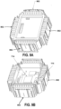
- FIGs. 9A and 9B are isometric views that illustrate that a grounding plate 802 may be integrated into each side of the integrated heatsink and antenna structure.
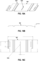
- FIGs. 10A-10C are illustrations of the grounding plate 802 in accordance with some embodiments.
- the grounding plate 802 may include ridges 1002 and slots 1004, any or all of which function to improve radio properties (e.g., radio patterns) of the RF antenna portions.
- the center slot 1004 illustrated in FIG. 10C may operate to improve the radio properties (e.g., radio patterns, etc.) of RF antenna portions of the integrated heatsink and antenna structure (e.g., by further tuning the antenna, etc.).
- a component may be, but is not limited to, a process running on a processor, a processor, an object, an executable, a thread of execution, a program, and/or a computer.
- a component may be, but is not limited to, a process running on a processor, a processor, an object, an executable, a thread of execution, a program, and/or a computer.
- an application running on a wireless device and the wireless device may be referred to as a component.
- One or more components may reside within a process and/or thread of execution and a component may be localized on one processor or core and/or distributed between two or more processors or cores.
- these components may execute from various non-transitory computer readable media having various instructions and/or data structures stored thereon.
- Components may communicate by way of local and/or remote processes, function or procedure calls, electronic signals, data packets, memory read/writes, and other known network, computer, processor, and/or process related communication methodologies.
- DSP digital signal processor
- ASIC application specific integrated circuit
- FPGA field programmable gate array
- a general-purpose processor may be a microprocessor, but, in the alternative, the processor may be any conventional processor, controller, microcontroller, or state machine.
- a processor may also be implemented as a combination of receiver smart objects, e.g., a combination of a DSP and a microprocessor, a plurality of microprocessors, one or more microprocessors in conjunction with a DSP core, or any other such configuration. Alternatively, some operations or methods may be performed by circuitry that is specific to a given function.
- the functions described may be implemented in hardware, software, firmware, or any combination thereof. If implemented in software, the functions may be stored as one or more instructions or code on a non-transitory computer-readable storage medium or non-transitory processor-readable storage medium.
- the operations of a method or algorithm disclosed herein may be embodied in a processor-executable software module or processor-executable instructions, which may reside on a non-transitory computer-readable or processor-readable storage medium.
- Non-transitory computer-readable or processor-readable storage media may be any storage media that may be accessed by a computer or a processor.
- non-transitory computer-readable or processor-readable storage media may include RAM, ROM, EEPROM, FLASH memory, CD-ROM or other optical disk storage, magnetic disk storage or other magnetic storage smart objects, or any other medium that may be used to store desired program code in the form of instructions or data structures and that may be accessed by a computer.
- Disk and disc includes compact disc (CD), laser disc, optical disc, digital versatile disc (DVD), floppy disk, and Blu-ray disc where disks usually reproduce data magnetically, while discs reproduce data optically with lasers. Combinations of the above are also included within the scope of non-transitory computer-readable and processor-readable media.
- the operations of a method or algorithm may reside as one or any combination or set of codes and/or instructions on a non-transitory processor-readable storage medium and/or computer-readable storage medium, which may be incorporated into a computer program product.
Landscapes
- Engineering & Computer Science (AREA)
- Computer Networks & Wireless Communication (AREA)
- Details Of Aerials (AREA)
- Cooling Or The Like Of Electrical Apparatus (AREA)
Claims (13)
- Dissipateur thermique intégré et structure d'antenne, comprenant :une partie d'antenne radiofréquence (120) ; etun partie de dissipateur thermique (140) couplée à au moins une extrémité d'un plan de masse (104) de la partie d'antenne radiofréquence (120), dans laquelle :la partie de dissipateur thermique (140) comprend une pluralité d'ailettes de dissipateur thermique (114) ;au moins une ailette de dissipateur thermique dans la pluralité d'ailettes de dissipateur thermique (114) comprend une languette (141) qui maintient le plan de masse (104) de la partie d'antenne radiofréquence (120) en place ;dans laquelle :la partie d'antenne radiofréquence est configurée pour améliorer les performances thermiques de la partie de dissipateur thermique ; etla partie de dissipateur thermique est configurée pour améliorer une ou plusieurs propriétés d'antenne de la partie d'antenne radiofréquence.
- Dissipateur thermique intégré et structure d'antenne selon la revendication 1, dans laquelle la pluralité d'ailettes de dissipateur thermique comprend des ailettes de dissipateur thermique flanquant le plan de masse sur des bords opposés de celui-ci.
- Dissipateur thermique intégré et structure d'antenne selon la revendication 1, dans laquelle la partie de dissipateur thermique est configurée pour modifier une ou plusieurs propriétés d'antenne de la partie d'antenne radiofréquence en modifiant une ou plusieurs des propriétés suivantes :les diagrammes de rayonnement de la partie d'antenne radiofréquence ;l'efficacité de rayonnement de la partie d'antenne radiofréquence ;la bande passante de la partie d'antenne radiofréquence ;l'impédance d'entrée de la partie d'antenne radiofréquence ;la polarisation de la partie d'antenne radiofréquence ;la directivité de la partie d'antenne radiofréquence ;le gain de la partie d'antenne radiofréquence ;la largeur du faisceau de la partie d'antenne radiofréquence ; oule rapport d'onde stationnaire de la partie d'antenne radiofréquence.
- Dissipateur thermique intégré et structure d'antenne selon la revendication 1, dans laquelle la partie d'antenne radiofréquence est configurée pour augmenter la surface du dissipateur thermique et la partie de dissipateur thermique est configurée pour étendre le plan de masse de la partie d'antenne radiofréquence de manière à modifier les diagrammes de rayonnement de la partie d'antenne radiofréquence.
- Dissipateur thermique intégré et structure d'antenne selon la revendication 1, dans laquelle la pluralité d'ailettes de dissipateur thermique comprend au moins une ailette de dissipateur thermique configurée pour fournir une charge capacitive à une extrémité ouverte d'un élément rayonnant de la partie d'antenne radiofréquence.
- Dissipateur thermique intégré et structure d'antenne selon la revendication 1, dans laquelle la partie d'antenne radiofréquence est configurée pour transmettre ou recevoir des communications sans fil et pour fournir un chemin pour dissiper l'énergie thermique ou la chaleur.
- Dissipateur thermique intégré et structure d'antenne selon la revendication 1, dans laquelle la partie d'antenne radiofréquence comprend plusieurs parties d'antenne radiofréquence séparées qui forment chacune une antenne en F inversé plane, PIFA.
- Dissipateur thermique intégré et structure d'antenne selon la revendication 7, dans laquelle la PIFA comprend :un composant d'alimentation; etun composant rayonnant qui comprend une partie court-circuitée et une partie rayonnante, la partie court-circuitée étant couplée au plan de masse de la partie d'antenne radiofréquence,dans laquelle :le composant d'alimentation engage le composant rayonnant à un point d'alimentation ; etla partie court-circuitée du composant rayonnant court-circuite électriquement une extrémité du composant rayonnant au plan de masse.
- Dissipateur thermique intégré et structure d'antenne selon la revendication 1, dans laquelle la partie d'antenne radiofréquence comprend plusieurs parties d'antenne radiofréquence séparées qui forment chacune une antenne monopolaire.
- Dissipateur thermique intégré et structure d'antenne selon la revendication 1, dans laquelle la partie d'antenne radiofréquence comprend un radiateur primaire configuré pour utiliser la partie de dissipateur thermique comme élément de mise en forme de champ pour produire un diagramme de rayonnement amélioré.
- Dissipateur thermique intégré et structure d'antenne selon la revendication 1, dans laquelle la totalité ou des parties du dissipateur thermique intégré et de la structure d'antenne est constituée d'aluminium ou de cuivre.
- Dissipateur thermique intégré et structure d'antenne selon la revendication 1, comprenant en outre :
une base de dissipateur thermique comprenant quatre surfaces latérales, dans laquelle :la partie d'antenne radiofréquence comprend multiples parties d'antenne radiofréquence, etchacune des multiples parties d'antenne radiofréquence est couplée à différentes surfaces des quatre surfaces latérales. - Dissipateur thermique intégré et structure d'antenne selon la revendication 12, dans laquelle :la base de dissipateur thermique comprend au moins une partie d'antenne radiofréquence supplémentaire montée entre les multiples parties d'antenne radiofréquence sur chacune des surfaces latérales ; ouchacune des multiples parties d'antenne radiofréquence comprend une plaque de mise à la terre fixée de manière fixe à l'une des quatre surfaces latérales.
Applications Claiming Priority (3)
| Application Number | Priority Date | Filing Date | Title |
|---|---|---|---|
| US201962945444P | 2019-12-09 | 2019-12-09 | |
| US17/110,744 US11563262B2 (en) | 2019-12-09 | 2020-12-03 | Integrated heatsink and antenna structure |
| PCT/US2020/063548 WO2021118907A1 (fr) | 2019-12-09 | 2020-12-07 | Dissipateur thermique intégré et structure d'antenne |
Related Child Applications (1)
| Application Number | Title | Priority Date | Filing Date |
|---|---|---|---|
| EP24222900.3 Division-Into | 2024-12-23 |
Publications (3)
| Publication Number | Publication Date |
|---|---|
| EP4073882A1 EP4073882A1 (fr) | 2022-10-19 |
| EP4073882B1 true EP4073882B1 (fr) | 2025-02-12 |
| EP4073882C0 EP4073882C0 (fr) | 2025-02-12 |
Family
ID=76211012
Family Applications (1)
| Application Number | Title | Priority Date | Filing Date |
|---|---|---|---|
| EP20829134.4A Active EP4073882B1 (fr) | 2019-12-09 | 2020-12-07 | Dissipateur thermique intégré et structure d'antenne |
Country Status (4)
| Country | Link |
|---|---|
| US (2) | US11563262B2 (fr) |
| EP (1) | EP4073882B1 (fr) |
| BR (1) | BR112022011117A2 (fr) |
| WO (1) | WO2021118907A1 (fr) |
Families Citing this family (8)
| Publication number | Priority date | Publication date | Assignee | Title |
|---|---|---|---|---|
| CN115706304A (zh) * | 2021-08-16 | 2023-02-17 | 华为技术有限公司 | 天线和网络设备 |
| USD1025047S1 (en) * | 2021-09-29 | 2024-04-30 | Veea Inc. | Computing device housing |
| USD1067233S1 (en) | 2021-09-24 | 2025-03-18 | Veea Inc. | Computing device housing |
| USD1028967S1 (en) * | 2021-09-28 | 2024-05-28 | Veea Inc. | Computing device housing |
| US11817624B1 (en) | 2021-10-01 | 2023-11-14 | Gregg Ehresmann | Ventilation apparatus for a containment of antenna elements |
| TWI897039B (zh) * | 2023-09-23 | 2025-09-11 | 啓碁科技股份有限公司 | 天線結構及電子裝置 |
| TWI873886B (zh) * | 2023-09-28 | 2025-02-21 | 啓碁科技股份有限公司 | 天線結構及電子裝置 |
| IL309781A (en) * | 2023-12-27 | 2025-07-01 | Elta Systems Ltd | Patch antenna with heat dissipation |
Family Cites Families (7)
| Publication number | Priority date | Publication date | Assignee | Title |
|---|---|---|---|---|
| WO2010148019A2 (fr) | 2009-06-15 | 2010-12-23 | Universit Of Florida Research Foundation, Inc. | Appareil et procédé pour une gestion thermique dans des antennes |
| US9209523B2 (en) | 2012-02-24 | 2015-12-08 | Futurewei Technologies, Inc. | Apparatus and method for modular multi-sector active antenna system |
| JP6520568B2 (ja) * | 2015-08-25 | 2019-05-29 | 住友電気工業株式会社 | アンテナ装置 |
| JP6525064B2 (ja) * | 2015-11-19 | 2019-06-05 | 日本電気株式会社 | 無線通信装置 |
| US10431868B2 (en) * | 2017-05-24 | 2019-10-01 | Plume Design, Inc. | Antenna structure incorporated in heat spreader, heat sink, and cooling fins |
| KR102489874B1 (ko) * | 2017-11-24 | 2023-01-18 | 삼성전자주식회사 | 방열 구조를 포함하는 전자 장치 |
| US10621503B1 (en) * | 2018-12-03 | 2020-04-14 | International Business Machines Corporation | Quantum computer hardware with reflectionless filters for thermalizing radio frequency signals |
-
2020
- 2020-12-03 US US17/110,744 patent/US11563262B2/en active Active
- 2020-12-07 EP EP20829134.4A patent/EP4073882B1/fr active Active
- 2020-12-07 BR BR112022011117A patent/BR112022011117A2/pt unknown
- 2020-12-07 WO PCT/US2020/063548 patent/WO2021118907A1/fr not_active Ceased
-
2022
- 2022-12-21 US US18/086,069 patent/US11949147B2/en active Active
Also Published As
| Publication number | Publication date |
|---|---|
| EP4073882A1 (fr) | 2022-10-19 |
| US20230126145A1 (en) | 2023-04-27 |
| BR112022011117A2 (pt) | 2022-08-23 |
| US20210175596A1 (en) | 2021-06-10 |
| WO2021118907A1 (fr) | 2021-06-17 |
| US11949147B2 (en) | 2024-04-02 |
| EP4073882C0 (fr) | 2025-02-12 |
| US11563262B2 (en) | 2023-01-24 |
Similar Documents
| Publication | Publication Date | Title |
|---|---|---|
| EP4073882B1 (fr) | Dissipateur thermique intégré et structure d'antenne | |
| US11837773B2 (en) | Resilient antenna securing mechanism | |
| US10299405B2 (en) | Mid-spreader for stacked circuit boards in an electronic device | |
| US20210234250A1 (en) | Antenna with Built-in Heatsink Structure | |
| US10461401B2 (en) | Antenna device and electronic device including the same | |
| CN103034291B (zh) | 终端设备 | |
| CN105009363B (zh) | 多天线系统 | |
| KR20220131335A (ko) | 안테나를 구비하는 전자 기기 | |
| JP2020517184A (ja) | 3スロット付きアンテナ装置及び方法 | |
| EP3905441A1 (fr) | Structure d'antenne et terminal de communication sans fil multibande haute fréquence | |
| CN110870139A (zh) | 多无线电、多通道(mrmc)网状网络设备的天线结构和隔离室 | |
| US10297921B2 (en) | Dipole antenna with cavity | |
| CN110199435A (zh) | 具有多天线系统的移动设备 | |
| US11575215B2 (en) | Antenna with enhanced azimuth gain | |
| US12183977B2 (en) | Antenna module and electronic device including same | |
| US11695438B2 (en) | Expandable architecture and bus for consumer gateway | |
| JP2007082179A (ja) | 多数のフィード点を有する組合せアンテナ | |
| EP2992568B1 (fr) | Système et procédé pour antenne mobile à fréquences de résonance et diagramme de rayonnement réglables | |
| Zhao et al. | Wideband internal antenna with coupled feeding for 4G mobile phone | |
| CN111799569B (zh) | 天线模组以及电子设备 | |
| Feng et al. | High performance resonant cavity antenna with non‐uniform metamaterial inspired superstrate | |
| Huang et al. | Miniaturized CPW‐Fed Triband Antenna with Asymmetric Ring for WLAN/WiMAX Applications | |
| CN114556701A (zh) | 天线装置 |
Legal Events
| Date | Code | Title | Description |
|---|---|---|---|
| STAA | Information on the status of an ep patent application or granted ep patent |
Free format text: STATUS: UNKNOWN |
|
| STAA | Information on the status of an ep patent application or granted ep patent |
Free format text: STATUS: THE INTERNATIONAL PUBLICATION HAS BEEN MADE |
|
| PUAI | Public reference made under article 153(3) epc to a published international application that has entered the european phase |
Free format text: ORIGINAL CODE: 0009012 |
|
| STAA | Information on the status of an ep patent application or granted ep patent |
Free format text: STATUS: REQUEST FOR EXAMINATION WAS MADE |
|
| 17P | Request for examination filed |
Effective date: 20220711 |
|
| AK | Designated contracting states |
Kind code of ref document: A1 Designated state(s): AL AT BE BG CH CY CZ DE DK EE ES FI FR GB GR HR HU IE IS IT LI LT LU LV MC MK MT NL NO PL PT RO RS SE SI SK SM TR |
|
| DAV | Request for validation of the european patent (deleted) | ||
| DAX | Request for extension of the european patent (deleted) | ||
| STAA | Information on the status of an ep patent application or granted ep patent |
Free format text: STATUS: EXAMINATION IS IN PROGRESS |
|
| 17Q | First examination report despatched |
Effective date: 20240313 |
|
| GRAP | Despatch of communication of intention to grant a patent |
Free format text: ORIGINAL CODE: EPIDOSNIGR1 |
|
| STAA | Information on the status of an ep patent application or granted ep patent |
Free format text: STATUS: GRANT OF PATENT IS INTENDED |
|
| RIC1 | Information provided on ipc code assigned before grant |
Ipc: H01Q 9/04 20060101ALI20240722BHEP Ipc: H01Q 1/24 20060101ALI20240722BHEP Ipc: H01Q 1/02 20060101AFI20240722BHEP |
|
| INTG | Intention to grant announced |
Effective date: 20240822 |
|
| GRAS | Grant fee paid |
Free format text: ORIGINAL CODE: EPIDOSNIGR3 |
|
| GRAA | (expected) grant |
Free format text: ORIGINAL CODE: 0009210 |
|
| STAA | Information on the status of an ep patent application or granted ep patent |
Free format text: STATUS: THE PATENT HAS BEEN GRANTED |
|
| AK | Designated contracting states |
Kind code of ref document: B1 Designated state(s): AL AT BE BG CH CY CZ DE DK EE ES FI FR GB GR HR HU IE IS IT LI LT LU LV MC MK MT NL NO PL PT RO RS SE SI SK SM TR |
|
| REG | Reference to a national code |
Ref country code: GB Ref legal event code: FG4D |
|
| REG | Reference to a national code |
Ref country code: CH Ref legal event code: EP |
|
| REG | Reference to a national code |
Ref country code: DE Ref legal event code: R096 Ref document number: 602020046037 Country of ref document: DE |
|
| REG | Reference to a national code |
Ref country code: IE Ref legal event code: FG4D |
|
| U01 | Request for unitary effect filed |
Effective date: 20250311 |
|
| U07 | Unitary effect registered |
Designated state(s): AT BE BG DE DK EE FI FR IT LT LU LV MT NL PT RO SE SI Effective date: 20250319 |
|
| PG25 | Lapsed in a contracting state [announced via postgrant information from national office to epo] |
Ref country code: RS Free format text: LAPSE BECAUSE OF FAILURE TO SUBMIT A TRANSLATION OF THE DESCRIPTION OR TO PAY THE FEE WITHIN THE PRESCRIBED TIME-LIMIT Effective date: 20250512 |
|
| PG25 | Lapsed in a contracting state [announced via postgrant information from national office to epo] |
Ref country code: PL Free format text: LAPSE BECAUSE OF FAILURE TO SUBMIT A TRANSLATION OF THE DESCRIPTION OR TO PAY THE FEE WITHIN THE PRESCRIBED TIME-LIMIT Effective date: 20250212 |
|
| PG25 | Lapsed in a contracting state [announced via postgrant information from national office to epo] |
Ref country code: ES Free format text: LAPSE BECAUSE OF FAILURE TO SUBMIT A TRANSLATION OF THE DESCRIPTION OR TO PAY THE FEE WITHIN THE PRESCRIBED TIME-LIMIT Effective date: 20250212 |
|
| PG25 | Lapsed in a contracting state [announced via postgrant information from national office to epo] |
Ref country code: NO Free format text: LAPSE BECAUSE OF FAILURE TO SUBMIT A TRANSLATION OF THE DESCRIPTION OR TO PAY THE FEE WITHIN THE PRESCRIBED TIME-LIMIT Effective date: 20250512 Ref country code: IS Free format text: LAPSE BECAUSE OF FAILURE TO SUBMIT A TRANSLATION OF THE DESCRIPTION OR TO PAY THE FEE WITHIN THE PRESCRIBED TIME-LIMIT Effective date: 20250612 |
|
| PG25 | Lapsed in a contracting state [announced via postgrant information from national office to epo] |
Ref country code: HR Free format text: LAPSE BECAUSE OF FAILURE TO SUBMIT A TRANSLATION OF THE DESCRIPTION OR TO PAY THE FEE WITHIN THE PRESCRIBED TIME-LIMIT Effective date: 20250212 |
|
| PG25 | Lapsed in a contracting state [announced via postgrant information from national office to epo] |
Ref country code: GR Free format text: LAPSE BECAUSE OF FAILURE TO SUBMIT A TRANSLATION OF THE DESCRIPTION OR TO PAY THE FEE WITHIN THE PRESCRIBED TIME-LIMIT Effective date: 20250513 |
|
| PG25 | Lapsed in a contracting state [announced via postgrant information from national office to epo] |
Ref country code: SM Free format text: LAPSE BECAUSE OF FAILURE TO SUBMIT A TRANSLATION OF THE DESCRIPTION OR TO PAY THE FEE WITHIN THE PRESCRIBED TIME-LIMIT Effective date: 20250212 |
|
| PG25 | Lapsed in a contracting state [announced via postgrant information from national office to epo] |
Ref country code: CZ Free format text: LAPSE BECAUSE OF FAILURE TO SUBMIT A TRANSLATION OF THE DESCRIPTION OR TO PAY THE FEE WITHIN THE PRESCRIBED TIME-LIMIT Effective date: 20250212 |
|
| PG25 | Lapsed in a contracting state [announced via postgrant information from national office to epo] |
Ref country code: SK Free format text: LAPSE BECAUSE OF FAILURE TO SUBMIT A TRANSLATION OF THE DESCRIPTION OR TO PAY THE FEE WITHIN THE PRESCRIBED TIME-LIMIT Effective date: 20250212 |
|
| PLBE | No opposition filed within time limit |
Free format text: ORIGINAL CODE: 0009261 |
|
| STAA | Information on the status of an ep patent application or granted ep patent |
Free format text: STATUS: NO OPPOSITION FILED WITHIN TIME LIMIT |
|
| 26N | No opposition filed |
Effective date: 20251113 |