EP4075155B1 - Procédé et appareil de mesure destinés à l'essai de matériaux d'une carte de stockage de données en forme de carte - Google Patents
Procédé et appareil de mesure destinés à l'essai de matériaux d'une carte de stockage de données en forme de carte Download PDFInfo
- Publication number
- EP4075155B1 EP4075155B1 EP22020170.1A EP22020170A EP4075155B1 EP 4075155 B1 EP4075155 B1 EP 4075155B1 EP 22020170 A EP22020170 A EP 22020170A EP 4075155 B1 EP4075155 B1 EP 4075155B1
- Authority
- EP
- European Patent Office
- Prior art keywords
- coil
- card
- data carrier
- pulse
- response
- Prior art date
- Legal status (The legal status is an assumption and is not a legal conclusion. Google has not performed a legal analysis and makes no representation as to the accuracy of the status listed.)
- Active
Links
Images


Classifications
-
- G—PHYSICS
- G06—COMPUTING OR CALCULATING; COUNTING
- G06K—GRAPHICAL DATA READING; PRESENTATION OF DATA; RECORD CARRIERS; HANDLING RECORD CARRIERS
- G06K7/00—Methods or arrangements for sensing record carriers, e.g. for reading patterns
- G06K7/10—Methods or arrangements for sensing record carriers, e.g. for reading patterns by electromagnetic radiation, e.g. optical sensing; by corpuscular radiation
- G06K7/10009—Methods or arrangements for sensing record carriers, e.g. for reading patterns by electromagnetic radiation, e.g. optical sensing; by corpuscular radiation sensing by radiation using wavelengths larger than 0.1 mm, e.g. radio-waves or microwaves
- G06K7/10118—Methods or arrangements for sensing record carriers, e.g. for reading patterns by electromagnetic radiation, e.g. optical sensing; by corpuscular radiation sensing by radiation using wavelengths larger than 0.1 mm, e.g. radio-waves or microwaves the sensing being preceded by at least one preliminary step
-
- G—PHYSICS
- G01—MEASURING; TESTING
- G01R—MEASURING ELECTRIC VARIABLES; MEASURING MAGNETIC VARIABLES
- G01R31/00—Arrangements for testing electric properties; Arrangements for locating electric faults; Arrangements for electrical testing characterised by what is being tested not provided for elsewhere
- G01R31/28—Testing of electronic circuits, e.g. by signal tracer
- G01R31/302—Contactless testing
- G01R31/315—Contactless testing by inductive methods
-
- G—PHYSICS
- G06—COMPUTING OR CALCULATING; COUNTING
- G06K—GRAPHICAL DATA READING; PRESENTATION OF DATA; RECORD CARRIERS; HANDLING RECORD CARRIERS
- G06K7/00—Methods or arrangements for sensing record carriers, e.g. for reading patterns
- G06K7/10—Methods or arrangements for sensing record carriers, e.g. for reading patterns by electromagnetic radiation, e.g. optical sensing; by corpuscular radiation
- G06K7/10009—Methods or arrangements for sensing record carriers, e.g. for reading patterns by electromagnetic radiation, e.g. optical sensing; by corpuscular radiation sensing by radiation using wavelengths larger than 0.1 mm, e.g. radio-waves or microwaves
- G06K7/10366—Methods or arrangements for sensing record carriers, e.g. for reading patterns by electromagnetic radiation, e.g. optical sensing; by corpuscular radiation sensing by radiation using wavelengths larger than 0.1 mm, e.g. radio-waves or microwaves the interrogation device being adapted for miscellaneous applications
Definitions
- the invention relates to a method for material testing of a card-shaped data carrier.
- Card-shaped data carriers are used in many areas, for example for carrying out cashless payment transactions, as identification documents or for proving access authorizations.
- a chip card has a card body and an integrated circuit embedded in the card body, for example in the form of a chip module with a chip. The chip module is inserted into a cavity or module opening in the card body.
- chip cards with an integrated coil that enable contactless or contactless communication.
- chip card controllers with RFID functionality can be used.
- the coil forms an oscillating circuit on the chip module with an additional capacitor.
- chip cards with dual interface (DI) functionality, where the card body of the chip card is made partly or completely of metal.
- DI dual interface
- a chip module is used which itself contains a coil (coil-on module). This coil couples to the metallic card body.
- An ID card may look optically correct, but determining the material or composition is not possible without mechanically or chemically destroying the structure.
- the EP 2765432 A2 describes a method for testing a circuit with an inductively coupling antenna for a terminal device, comprising the following steps: The circuit is excited to oscillate using an energy pulse. In a further step, the oscillation of the circuit is detected in response to the excitation of the circuit by the energy pulse. The detected oscillation of the circuit is finally evaluated, in particular with regard to a natural resonance frequency of the circuit.
- the step of evaluating the detected oscillation can be carried out as a function of a field strength (H) in which the circuit is located.
- the steps of generating an alternating magnetic field of predetermined field strength (H) and arranging the circuit in the alternating field can be carried out before the step of exciting the circuit.
- the detection of the oscillation of the circuit can be carried out using a broadband measuring antenna.
- the EP 2779031 A2 describes a method for measuring a property of an oscillating circuit intended for contactless data communication and a corresponding measuring device.
- the measuring device is guided to the oscillating circuit.
- the oscillating circuit is excited by the measuring device using an energy pulse and a decaying oscillation of the oscillating circuit in response to the excitation by the energy pulse is recorded with the measuring device.
- the measuring device comprises a handle for guiding the measuring device, an excitation antenna for the exciting energy pulse and a measuring antenna for recording the decaying oscillation.
- the object of the present invention is therefore to improve the control of a card-shaped data carrier.
- the parameter can be a physical parameter such as voltage or time or even a mathematical parameter such as a mean or an integral.
- An oscillating circuit is also understood here to be an open oscillating circuit with only one coil and the parasitic capacitance (C p ) that forms around the oscillating circuit.
- the oscillating circuit is influenced by the parasitic capacitance (C DuT ) of the material or structure to be tested.
- a test procedure can include exciting the coil to be tested to oscillate, recording the free, damped oscillation of the coil in response to the excitation, and evaluating the recorded oscillation.
- a Dirac measuring system (DiraTest ® measuring system) can be used as a measuring device.
- the measuring head is modified so that, for example, a card with RFID properties is firmly attached under the measuring head. A measurement is thus made possible using a simple reference card.
- the method proposed here has the advantage that card-shaped data carriers can be examined or tested easily and quickly and, above all, non-destructively.
- the reference oscillating circuit is calibrated by sending out a pulse, detecting a vibration response of the coil in response to the pulse and determining at least one calibration parameter from the vibration response and that the material and/or composition of the data carrier is determined based on the at least one specific parameter relative to at least one calibration parameter. This allows a comparison of individual measurement points in relation to the individual measurement points. In this way, a relative deviation between individual measurement points can be determined and conclusions can be drawn from this about the material and/or structure of a tested data carrier.
- the material and/or composition of the data carrier is determined absolutely based on the at least one specific parameter and a specified material and/or composition of the data carrier. In this way, absolute values can be determined.
- Information on the material and/or structure of a data carrier can be given at one or more reference points. Calibration then takes place at this or these reference points. The material and/or structure of a data carrier can then be determined at all measuring points by converting the deviation of the measured values at the measuring points.
- the transmission and detection take place without contact. Since electromagnetic pulses are used, the data carrier can be measured from a defined distance that makes measurements comparable. The data carrier thus remains without contact, so that the data carrier is not affected.
- the coil is part of an RFID transponder. Due to the widespread use, suitable measuring systems are available and accurate and comparable measurement results can be achieved.
- the reference oscillating circuit can be designed to have a coil, a capacitor and a resistor. This creates a defined oscillating circuit, which can simplify the comparability of measurements.
- the reference resonant circuit has a coil and a capacitor of an integrated circuit of the data carrier.
- the reference resonant circuit can thus be designed as a reference data carrier. In this way, identical electromagnetic properties as on a card-shaped data carrier can be created during measurement or material testing or quality control.
- At least one parameter is selected from the group of resonance frequency, quality, amplitude and mean error.
- these parameters individually and in combination, are well suited to characterizing the material or the card-shaped data carrier.
- a signature of the material or the card-shaped data carrier can be generated, which enables recognition and comparison.
- the quality of the coil is determined from a decay coefficient of the oscillation response.
- the quality of the coil or antenna coil can be determined from the decay coefficient ⁇ . The longer the decay process lasts, the higher the quality of the corresponding oscillating circuit. This allows an evaluation of the free damped oscillation of the coil, i.e. its decay immediately after excitation to determine the quality and also the natural resonance frequency of the coil.
- a measuring device for material testing of a card-shaped data carrier designed to emit a pulse of an electromagnetic oscillation and to detect an oscillation response of the coil in response to the pulse, comprises a measuring head and a reference oscillating circuit with a coil, which is arranged on the measuring head, wherein the reference oscillating circuit can be trimmed by means of at least one capacitor.
- trimmable reference resonant circuit uses the trimmable reference resonant circuit to traversed during a measurement. This allows frequency-dependent characteristics of the materials to be tested to be taken into account. This can increase the accuracy and significance of the measurement.
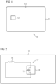
- Fig. 1 shows as an example of a card-shaped data carrier a chip card 10 with a card body 11.
- the card body 11 can consist of a plastic such as PVC, polycarbonate or similar.
- the thickness of the card body 11 can be, for example, between 50 ⁇ m and 920 ⁇ m.
- the chip card 10 further comprises a chip module 12 which is inserted into a main surface 13 of the card body 11 or the chip card 10.
- the chip module 12 can be inserted into a module opening or cavity.
- the cavity can comprise a central blind hole and a peripheral edge area. Here, the cavity is covered by the inserted chip module 12.
- the chip module 12 can be glued in the cavity.
- the chip module 12 comprises a coil that can be arranged on a module tape (not shown here).
- the coil can have approximately 12 to 16 turns, which here run concentrically around a chip or an electronic circuit of the chip module 12.
- the width of a turn can be 50 ⁇ m to 70 ⁇ m and the distance between two turns can be 100 ⁇ m.
- the turns can have copper thicknesses of up to approximately 30 ⁇ m. A maximum of 2.5 ⁇ H can be achieved with such a coil.
- the chip can be implemented in the form of an integrated circuit, for example, and is attached to an underside of the chip module 12 in a potting compound, for example.
- the chip is supplied with energy and/or signals via the coil.
- An electromagnetic field can be coupled into the coil.
- the chip can be a chip card controller with RFID functionality or contain it.
- Fig. 2 shows an equivalent circuit diagram of the chip module 12 of the chip card 10.
- the chip module 12 includes the chip 14, for example in the form of an integrated circuit.
- the chip 14 can be soldered onto the chip module 12, for example, or attached to the chip module 12 using flip-chip assembly.
- the chip 14 contains a card controller for the chip card 10.
- the chip 14 usually contains a processor for carrying out control functions for the chip card 10 and for communication and for carrying out computing operations, for example for security functions.
- the chip 14 contains a memory area for storing and/or making data available.
- the chip 14 also contains a capacitor 15 with a capacitance of, for example, 78 pF.
- the coil 16 is connected in parallel to the chip 14 and has a maximum inductance of 2.5 ⁇ H.
- the coil 16 and the capacitor 15 of the chip 14 form an oscillating circuit 17.
- the chip module 12 can communicate with a reader or a measuring device external to the chip card 10.
- the reader introduces energy into the coil 16 via an electromagnetic field, which activates the chip 14.
- the chip card 10 can be used as a measuring device with a reference oscillating circuit 17. This chip card 10 can then be used to measure other chip cards or similar.
- Fig. 3 shows an equivalent circuit diagram of a chip module 12 of the chip card with a reference resonant circuit in the form of an open resonant circuit 17.
- the open resonant circuit 17 is represented by the two contact points 18.
- the capacitor 15 shown here corresponds to the capacitance of a card-shaped data carrier to be tested when it is arranged on the chip module 12 or the measuring device.
- the data carrier can be placed directly on the two contact points 18 or can be arranged a short distance from them. The short distance is in the range of millimeters to a few centimeters.
- a parasitic capacitance 15a is present in parallel with the capacitor 15.
- This parasitic capacitance 15a is formed by the coil 16 and the material in which the coil 16 is located.
- the parasitic capacitance is also present, but is negligible in the closed resonant circuits there.
- this structure has a resonant frequency of between 45 MHz and 75 MHz.
- the frequency is determined exclusively by the inductance L of the coil 16 and the parasitic capacitance 15a from the coil 16 and the material carrier of the coil 16.
- a change in the capacitor 15 causes a significant change in the resonant circuit 17.
- the capacitance is, for example, between 1 pF and 3 pF.
- a circuit board or a similar carrier can also be used for the oscillating circuit 17.
- the form factor of the measuring head can then be smaller.
- Fig. 4 shows an equivalent circuit diagram of a chip module 12 of the chip card with an oscillating circuit 17 with capacitor 15, coil 16 and resistor 19.
- the oscillating circuit 17 is formed without the object to be tested.
- the object to be tested changes the oscillating circuit through its presence as previously described.
- a circuit board or a similar carrier can also be used for the oscillating circuit 17.
- the form factor of the measuring head can then be smaller.
- the capacitance of the capacitor 15 can be in a range from 1 pF to about 100 pF.
- the value of the resistor 19 can be in a range from about 0 ohms to 5 kOhms.
- the oscillating circuit 17 can therefore also be constructed without a resistor.
- Fig. 5 shows a basic representation of a measuring device 20 for material testing of a card-shaped data carrier, here in the form of a chip card 10.
- the chip card 10 is shown enlarged. While only the chip card 10 is referred to below for reasons of clarity, all card-shaped data carriers are included.
- the measuring device 20 may be a pulse measuring device with a measuring head 21 arranged to emit a pulse of an electromagnetic oscillation and to detect an oscillation response of the oscillating circuit 17 in response to the pulse.
- the measuring head 21 or the measuring device 20 is set up to excite the reference oscillating circuit 17 to oscillate.
- An evaluation device 22 of the measuring device 20 is set up to evaluate an oscillation of the reference oscillating circuit 17 detected in response to the excitation by the measuring head 21 or the measuring device 20.
- the oscillation behavior of the reference oscillating circuit 17 changes depending on the material and/or the structure, such as a layer sequence of the chip card 10.
- the resonance frequency, the quality and the amplitude of the vibration response or of the antenna coil can be determined in a simple and reliable manner. An evaluation of these parameters then allows conclusions to be drawn about the material and/or the composition of the chip card 10.
- At least one of the parameters resonance frequency, quality and amplitude from the vibration response is used to characterize the chip card 10. The more parameters are used, the more accurately the measurement or test can be carried out.
- a feature matrix can be set up in which the three parameters resonance frequency, quality and amplitude are plotted against different materials or layer sequences of a chip card 10.
- the measuring device 20 can, for example, be a test device for testing the functionality of the coil 16 for a contactless communicating chip card 10 or can comprise such a test device.
- the measuring device 20 comprises a pulse generator 23. This is set up to excite the reference oscillating circuit 17 in a contactless manner via an excitation coil 24 connected to the pulse generator 23.
- the measuring device 20 comprises a measuring antenna 25, which, like the excitation coil 24, can be arranged in the measuring head 21.
- a test device can thus be used to test the functionality of the coil 16 for the material testing of the chip card 10.
- the measuring head 21 is expanded with the reference oscillating circuit 17.
- the chip card 10 to be measured then changes the oscillating circuit 17, which is then measured.
- the measuring head 21 and the reference oscillating circuit 17 form a measuring unit for the chip card 10.
- the reference oscillating circuit 17 is used as a sensor for the chip card 10.
- the reference oscillating circuit 17 can be part of another chip card not shown here. This other chip card not shown here is then used as a sensor for the chip card 10.
- the measuring antenna 25 is designed to detect a free, damped oscillation of the reference resonant circuit 17 without contact.
- the evaluation device 22 is connected to the measuring antenna 25 and designed to evaluate the free, damped oscillation detected by the measuring antenna 25.
- the chip card 10 can be arranged on a base with a low dielectric constant of less than 10, preferably less than 5.
- a POM plate can be used as a base. This material has a very low dielectric constant of around 4, which is also constant over the entire surface of the plate. This creates a defined environment that increases the test quality and makes different test runs more comparable.
- the chip card 10 can also be stored in air or as far in air as possible, for example using thin bands such as fishing line. This allows the dielectric constant behind the chip card 10 to be further reduced.
- the measurement or material testing may include moving the chip card 10 and/or the measuring head 21 to a single measuring point or moving or traveling along a movement route.
- individual measuring points can also be approached or the chip card 10 can, for example, be moved past one or more stationary measuring heads during production.
- individual measuring points are specified in a sense via the time interval, which can then lie on a movement route.
- the reference resonant circuit 17 can, for example, be trimmed using at least one capacitor. This allows different frequency bands to be traversed during a measurement. This allows frequency-dependent characteristics of the materials to be tested to be taken into account.
- Fig. 6 shows a flow chart of a method for material testing of a card-shaped data carrier, for example in the form of a chip card 10.
- the reference oscillating circuit 17 is arranged on a measuring head 21 of the pulse measuring device 20.
- the reference oscillating circuit 17 is attached to the measuring head 21 in a defined manner, for example as part of a reference chip card, so that a clear position relative to the measuring head 21 is achieved.
- the coil 16 of the reference oscillating circuit 17 and the excitation coil 24 of the measuring head 21 are arranged parallel and overlapping, preferably one above the other, i.e. completely overlapping.
- the reference oscillating circuit 17 and the measuring head 21 are arranged in such a way that a pulse of an electromagnetic oscillation is transmitted from the excitation coil 24 to the coil 16 is possible and that it is possible to detect an oscillation response of the coil 16 in response to the pulse.
- calibration can be carried out by sending out a pulse, recording an oscillation response of the coil 16 or the reference oscillating circuit 17 in response to the pulse and determining at least one calibration parameter resonance frequency, quality and amplitude from the oscillation response.
- the quality of the coil 16 can be determined, for example, from a decay coefficient ⁇ of the oscillation response. The longer the decay process, the higher the quality of the corresponding oscillating circuit. Thus, an evaluation of the free damped oscillation of the coil 16, i.e. its decay immediately after excitation, allows the quality and also the natural resonance frequency of the coil 16 to be determined.
- the amplitude can, for example, be determined simply as the maximum amplitude.
- the calibration of the reference oscillating circuit 17 can be carried out in the open air, i.e. without the presence of a material in the vicinity of the measuring head 21.
- Known materials, data carriers or layer sequences of materials can also be calibrated. These materials etc. are then arranged on the measuring head 21 for a measurement.
- a second step 110 the reference oscillating circuit 17 is moved relative to at least one measuring point on the chip card 10.
- the reference oscillating circuit 17 is moved together with the measuring head 21.
- the measurement or material testing can be carried out in a movement route over the surface of the chip card 10 or purely at specific points.
- a pulse is sent out, a vibration response of the coil 16 is recorded in response to the pulse and one of the parameters resonance frequency, quality and amplitude is recorded from the vibration response.
- This step is analogous to the optional calibration step, whereby the chip card 10 present in the area of the reference resonant circuit 17 now changes the vibration response of the coil 16.
- the reference resonant circuit 17 changes when there is a capacitive influence from material in the area of the measuring head 21. If, for example, an additional capacitance is introduced into the resonant circuit 17, the frequency drops significantly and the Q factor drops slightly.
- each form of data carrier, intermediate product of data carrier or material an identification can be created based on at least one of the parameters resonance frequency, quality and amplitude. This assignment of parameter values and materials or compositions can be stored in a list or matrix.
- the material and/or composition of the data carrier is determined based on at least one of the determined parameters. For this purpose, for example, current values of the determined parameter(s) can be compared with a list or matrix in which an assignment of parameter values and materials or compositions is stored.
- the measuring points can come from one or more measuring objects.
- quantities or sub-parameters such as a maximum value, minimum value and average value or spatial progression of the parameters can be determined from the individual parameters. These quantities can, for example, be used to identify materials or compositions.
Landscapes
- Physics & Mathematics (AREA)
- Engineering & Computer Science (AREA)
- Health & Medical Sciences (AREA)
- Toxicology (AREA)
- General Physics & Mathematics (AREA)
- Electromagnetism (AREA)
- General Health & Medical Sciences (AREA)
- Artificial Intelligence (AREA)
- Computer Vision & Pattern Recognition (AREA)
- Theoretical Computer Science (AREA)
- General Engineering & Computer Science (AREA)
- Credit Cards Or The Like (AREA)
Claims (8)
- Procédé d'essai de matériau d'un support de données (10) sous forme de carte, comprenant les étapes consistant à :- disposer (100) un circuit oscillant de référence (17) présentant une bobine (16) sur une tête de mesure (21) d'un appareil de mesure à impulsion (20) qui est conçu pour émettre une impulsion d'une oscillation électromagnétique et pour détecter une réponse en oscillation de la bobine (16) en réaction à l'impulsion ;- déplacer (120) relativement le circuit oscillant de référence (17) par rapport au support de données (10) ;- émettre (130) une impulsion, détecter une réponse en oscillation de la bobine (16) en réaction à l'impulsion, et déterminer au moins un paramètre à partir de la réponse en oscillation ; et- établir (140) un matériau et/ou une composition du support de données (10) sur la base dudit au moins un paramètre déterminé.
- Procédé selon la revendication 1, caractérisé en ce qu'un étalonnage du circuit oscillant de référence (17) est effectué par l'émission d'une impulsion, la détection d'une réponse en oscillation de la bobine (16) en réaction à l'impulsion, et la détermination d'au moins un paramètre d'étalonnage à partir de la réponse en oscillation, et en ce que l'établissement du matériau et/ou de la composition du support de données (10) est effectué sur la base dudit au moins un paramètre déterminé par rapport audit au moins un paramètre d'étalonnage.
- Procédé selon l'une quelconque des revendications 1 à 2, caractérisé en ce qu'une qualité de la bobine (16) est établie à partir d'un coefficient d'évanouissement (δ) de la réponse en oscillation.
- Procédé selon l'une quelconque des revendications 1 à 3, caractérisé en ce que l'émission et la détection sont effectuées sans contact.
- Procédé selon l'une quelconque des revendications 1 à 4, caractérisé en ce que la bobine (16) fait partie d'un transpondeur RFID.
- Procédé selon l'une quelconque des revendications 1 à 5, caractérisé en ce que le circuit oscillant de référence (17) présente la bobine (16), un condensateur (15) et une résistance (19).
- Procédé selon l'une quelconque des revendications 1 à 6, caractérisé en ce que le circuit oscillant de référence (17) présente la bobine (16) et un condensateur (15) d'un circuit intégré du support de données (10).
- Procédé selon l'une quelconque des revendications 1 à 7, caractérisé en ce que ledit au moins un paramètre est sélectionné dans le groupe de la fréquence de résonance, de la qualité, de l'amplitude et de l'erreur quadratique moyenne.
Applications Claiming Priority (1)
| Application Number | Priority Date | Filing Date | Title |
|---|---|---|---|
| DE102021001965.2A DE102021001965A1 (de) | 2021-04-14 | 2021-04-14 | Verfahren und Messgerät zur Materialprüfung eines kartenförmigen Datenträgers |
Publications (2)
| Publication Number | Publication Date |
|---|---|
| EP4075155A1 EP4075155A1 (fr) | 2022-10-19 |
| EP4075155B1 true EP4075155B1 (fr) | 2024-12-18 |
Family
ID=81580456
Family Applications (1)
| Application Number | Title | Priority Date | Filing Date |
|---|---|---|---|
| EP22020170.1A Active EP4075155B1 (fr) | 2021-04-14 | 2022-04-13 | Procédé et appareil de mesure destinés à l'essai de matériaux d'une carte de stockage de données en forme de carte |
Country Status (2)
| Country | Link |
|---|---|
| EP (1) | EP4075155B1 (fr) |
| DE (1) | DE102021001965A1 (fr) |
Families Citing this family (1)
| Publication number | Priority date | Publication date | Assignee | Title |
|---|---|---|---|---|
| DE102024105661A1 (de) * | 2024-02-28 | 2025-08-28 | Giesecke+Devrient ePayments GmbH | Verfahren und Vorrichtung zum Bestimmen der Resonanzfrequenz einer Chipkarte |
Family Cites Families (3)
| Publication number | Priority date | Publication date | Assignee | Title |
|---|---|---|---|---|
| DE102012002884A1 (de) | 2012-02-14 | 2013-08-14 | Giesecke & Devrient Gmbh | Verfahren und Vorrichtung zum kontaktlosen Prüfen eines flächigen Sicherheitsdokuments |
| DE102013002138A1 (de) * | 2013-02-07 | 2014-08-07 | Giesecke & Devrient Gmbh | Verfahren und Vorrichtung zum Prüfen eines Schaltkreises eines Endgeräts |
| DE102013004194A1 (de) * | 2013-03-12 | 2014-09-18 | Giesecke & Devrient Gmbh | Messverfahren und Messvorrichtung |
-
2021
- 2021-04-14 DE DE102021001965.2A patent/DE102021001965A1/de active Pending
-
2022
- 2022-04-13 EP EP22020170.1A patent/EP4075155B1/fr active Active
Also Published As
| Publication number | Publication date |
|---|---|
| DE102021001965A1 (de) | 2022-10-20 |
| EP4075155A1 (fr) | 2022-10-19 |
Similar Documents
| Publication | Publication Date | Title |
|---|---|---|
| DE60103742T2 (de) | Modul zur leistungsbewertung eines rf-identifizierungsetiketts (rfid) | |
| EP2954338B1 (fr) | Procédé et dispositif pour tester un circuit de commutation | |
| EP2754086B1 (fr) | Methode pour tester une bobine d'antenne | |
| DE10232398A1 (de) | Verfahren und Vorrichtung zur Inspektion von Leiterplatten | |
| EP1381874B1 (fr) | Procede et dispositif pour tester sans contact une antenne non equipee | |
| EP4226170B1 (fr) | Dispositif de contrôle d'authenticité d'un support de données à caractéristique rmn à champ nul | |
| EP4075155A1 (fr) | Procédé et appareil de mesure destinés à l'essai de matériaux d'une carte de stockage de données en forme de carte | |
| EP1779057B1 (fr) | Procede de determination sans contact d'une epaisseur de couche par mesure de la resistance et de l'inductance d'une bobine de capteur | |
| DE102013110017A1 (de) | Vorrichtung und Verfahren zur Klassifikation und Identifikation mit einer RFID-Leseeinrichtung | |
| EP2581984B1 (fr) | Procédé de contrôle d'une bobine-antenne | |
| EP2779031B1 (fr) | Procédé de mesure et dispositif de mesure | |
| EP3070636B1 (fr) | Indicateur de champ de lecture destiné à vérifier le champ de lecture d'un lecteur rfid | |
| EP2722794A2 (fr) | Vérification d'un circuit de commutation | |
| EP2815387B1 (fr) | Procédé et dispositif de contrôle sans contact d'un document de sécurité plan | |
| EP4075322B1 (fr) | Procédé de contrôle de la qualité d'une feuille métallique d'un corps de carte | |
| DE212009000026U1 (de) | Verbindungssensor zur Identifikation einer Anschlussstelle in einer Schalttafel | |
| EP4315156B1 (fr) | Procédé de détermination d'une valeur d'intensité de champ électromagnétique, procédé de couplage d'un appareil de lecture, carte à puce et appareil de lecture pour carte à puce | |
| DE3013611A1 (de) | Verfahren und vorrichtung zum identifizieren von muenzen o.dgl. | |
| DE102005006853B4 (de) | Messsystem und Verfahren zur Ankopplung eines Sensorelements in dem Messsystem | |
| DE102013002138A1 (de) | Verfahren und Vorrichtung zum Prüfen eines Schaltkreises eines Endgeräts | |
| DE102013002140A1 (de) | Verfahren und Vorrichtung zum Bestimmen einer Schaltkreiseigenschaft | |
| WO2025180557A1 (fr) | Procédé et dispositif de détermination de la fréquence de résonance d'une carte à puce | |
| DE102013002139A1 (de) | Verfahren und Vorrichtung zum Prüfen eines Schaltkreises | |
| DE102020212475A1 (de) | Sensorvorrichtung und Verfahren zur Bestimmung einer Eigenschaft einer Magnetisierung einer Sensorstruktur für eine Drehmomenterkennung | |
| DE102024130007A1 (de) | Verfahren und Lokalisierungsvorrichtung zum Lokalisieren einer verdeckt in einem Halbfabrikat angeordneten Antennenspule sowie Herstellungsanlage |
Legal Events
| Date | Code | Title | Description |
|---|---|---|---|
| PUAI | Public reference made under article 153(3) epc to a published international application that has entered the european phase |
Free format text: ORIGINAL CODE: 0009012 |
|
| STAA | Information on the status of an ep patent application or granted ep patent |
Free format text: STATUS: THE APPLICATION HAS BEEN PUBLISHED |
|
| AK | Designated contracting states |
Kind code of ref document: A1 Designated state(s): AL AT BE BG CH CY CZ DE DK EE ES FI FR GB GR HR HU IE IS IT LI LT LU LV MC MK MT NL NO PL PT RO RS SE SI SK SM TR |
|
| STAA | Information on the status of an ep patent application or granted ep patent |
Free format text: STATUS: REQUEST FOR EXAMINATION WAS MADE |
|
| RAP3 | Party data changed (applicant data changed or rights of an application transferred) |
Owner name: GIESECKE+DEVRIENT MOBILE SECURITY GMBH |
|
| 17P | Request for examination filed |
Effective date: 20230419 |
|
| RBV | Designated contracting states (corrected) |
Designated state(s): AL AT BE BG CH CY CZ DE DK EE ES FI FR GB GR HR HU IE IS IT LI LT LU LV MC MK MT NL NO PL PT RO RS SE SI SK SM TR |
|
| P01 | Opt-out of the competence of the unified patent court (upc) registered |
Effective date: 20230519 |
|
| STAA | Information on the status of an ep patent application or granted ep patent |
Free format text: STATUS: EXAMINATION IS IN PROGRESS |
|
| 17Q | First examination report despatched |
Effective date: 20230725 |
|
| RAP3 | Party data changed (applicant data changed or rights of an application transferred) |
Owner name: GIESECKE+DEVRIENT EPAYMENTS GMBH |
|
| GRAP | Despatch of communication of intention to grant a patent |
Free format text: ORIGINAL CODE: EPIDOSNIGR1 |
|
| STAA | Information on the status of an ep patent application or granted ep patent |
Free format text: STATUS: GRANT OF PATENT IS INTENDED |
|
| INTG | Intention to grant announced |
Effective date: 20241008 |
|
| GRAS | Grant fee paid |
Free format text: ORIGINAL CODE: EPIDOSNIGR3 |
|
| GRAA | (expected) grant |
Free format text: ORIGINAL CODE: 0009210 |
|
| STAA | Information on the status of an ep patent application or granted ep patent |
Free format text: STATUS: THE PATENT HAS BEEN GRANTED |
|
| AK | Designated contracting states |
Kind code of ref document: B1 Designated state(s): AL AT BE BG CH CY CZ DE DK EE ES FI FR GB GR HR HU IE IS IT LI LT LU LV MC MK MT NL NO PL PT RO RS SE SI SK SM TR |
|
| REG | Reference to a national code |
Ref country code: CH Ref legal event code: EP |
|
| REG | Reference to a national code |
Ref country code: DE Ref legal event code: R096 Ref document number: 502022002391 Country of ref document: DE |
|
| REG | Reference to a national code |
Ref country code: IE Ref legal event code: FG4D Free format text: LANGUAGE OF EP DOCUMENT: GERMAN |
|
| REG | Reference to a national code |
Ref country code: LT Ref legal event code: MG9D |
|
| PG25 | Lapsed in a contracting state [announced via postgrant information from national office to epo] |
Ref country code: HR Free format text: LAPSE BECAUSE OF FAILURE TO SUBMIT A TRANSLATION OF THE DESCRIPTION OR TO PAY THE FEE WITHIN THE PRESCRIBED TIME-LIMIT Effective date: 20241218 |
|
| PG25 | Lapsed in a contracting state [announced via postgrant information from national office to epo] |
Ref country code: FI Free format text: LAPSE BECAUSE OF FAILURE TO SUBMIT A TRANSLATION OF THE DESCRIPTION OR TO PAY THE FEE WITHIN THE PRESCRIBED TIME-LIMIT Effective date: 20241218 |
|
| PG25 | Lapsed in a contracting state [announced via postgrant information from national office to epo] |
Ref country code: BG Free format text: LAPSE BECAUSE OF FAILURE TO SUBMIT A TRANSLATION OF THE DESCRIPTION OR TO PAY THE FEE WITHIN THE PRESCRIBED TIME-LIMIT Effective date: 20241218 |
|
| PG25 | Lapsed in a contracting state [announced via postgrant information from national office to epo] |
Ref country code: NO Free format text: LAPSE BECAUSE OF FAILURE TO SUBMIT A TRANSLATION OF THE DESCRIPTION OR TO PAY THE FEE WITHIN THE PRESCRIBED TIME-LIMIT Effective date: 20250318 |
|
| REG | Reference to a national code |
Ref country code: NL Ref legal event code: MP Effective date: 20241218 |
|
| PG25 | Lapsed in a contracting state [announced via postgrant information from national office to epo] |
Ref country code: LV Free format text: LAPSE BECAUSE OF FAILURE TO SUBMIT A TRANSLATION OF THE DESCRIPTION OR TO PAY THE FEE WITHIN THE PRESCRIBED TIME-LIMIT Effective date: 20241218 Ref country code: GR Free format text: LAPSE BECAUSE OF FAILURE TO SUBMIT A TRANSLATION OF THE DESCRIPTION OR TO PAY THE FEE WITHIN THE PRESCRIBED TIME-LIMIT Effective date: 20250319 |
|
| PG25 | Lapsed in a contracting state [announced via postgrant information from national office to epo] |
Ref country code: RS Free format text: LAPSE BECAUSE OF FAILURE TO SUBMIT A TRANSLATION OF THE DESCRIPTION OR TO PAY THE FEE WITHIN THE PRESCRIBED TIME-LIMIT Effective date: 20250318 |
|
| PG25 | Lapsed in a contracting state [announced via postgrant information from national office to epo] |
Ref country code: NL Free format text: LAPSE BECAUSE OF FAILURE TO SUBMIT A TRANSLATION OF THE DESCRIPTION OR TO PAY THE FEE WITHIN THE PRESCRIBED TIME-LIMIT Effective date: 20241218 |
|
| PG25 | Lapsed in a contracting state [announced via postgrant information from national office to epo] |
Ref country code: SM Free format text: LAPSE BECAUSE OF FAILURE TO SUBMIT A TRANSLATION OF THE DESCRIPTION OR TO PAY THE FEE WITHIN THE PRESCRIBED TIME-LIMIT Effective date: 20241218 |
|
| PG25 | Lapsed in a contracting state [announced via postgrant information from national office to epo] |
Ref country code: PL Free format text: LAPSE BECAUSE OF FAILURE TO SUBMIT A TRANSLATION OF THE DESCRIPTION OR TO PAY THE FEE WITHIN THE PRESCRIBED TIME-LIMIT Effective date: 20241218 |
|
| PGFP | Annual fee paid to national office [announced via postgrant information from national office to epo] |
Ref country code: DE Payment date: 20250519 Year of fee payment: 4 |
|
| PG25 | Lapsed in a contracting state [announced via postgrant information from national office to epo] |
Ref country code: ES Free format text: LAPSE BECAUSE OF FAILURE TO SUBMIT A TRANSLATION OF THE DESCRIPTION OR TO PAY THE FEE WITHIN THE PRESCRIBED TIME-LIMIT Effective date: 20241218 |
|
| PG25 | Lapsed in a contracting state [announced via postgrant information from national office to epo] |
Ref country code: IS Free format text: LAPSE BECAUSE OF FAILURE TO SUBMIT A TRANSLATION OF THE DESCRIPTION OR TO PAY THE FEE WITHIN THE PRESCRIBED TIME-LIMIT Effective date: 20250418 |
|
| PG25 | Lapsed in a contracting state [announced via postgrant information from national office to epo] |
Ref country code: PT Free format text: LAPSE BECAUSE OF FAILURE TO SUBMIT A TRANSLATION OF THE DESCRIPTION OR TO PAY THE FEE WITHIN THE PRESCRIBED TIME-LIMIT Effective date: 20250421 |
|
| PG25 | Lapsed in a contracting state [announced via postgrant information from national office to epo] |
Ref country code: EE Free format text: LAPSE BECAUSE OF FAILURE TO SUBMIT A TRANSLATION OF THE DESCRIPTION OR TO PAY THE FEE WITHIN THE PRESCRIBED TIME-LIMIT Effective date: 20241218 |
|
| PGFP | Annual fee paid to national office [announced via postgrant information from national office to epo] |
Ref country code: FR Payment date: 20250424 Year of fee payment: 4 |
|
| PG25 | Lapsed in a contracting state [announced via postgrant information from national office to epo] |
Ref country code: RO Free format text: LAPSE BECAUSE OF FAILURE TO SUBMIT A TRANSLATION OF THE DESCRIPTION OR TO PAY THE FEE WITHIN THE PRESCRIBED TIME-LIMIT Effective date: 20241218 |
|
| PGFP | Annual fee paid to national office [announced via postgrant information from national office to epo] |
Ref country code: AT Payment date: 20250721 Year of fee payment: 4 |
|
| PG25 | Lapsed in a contracting state [announced via postgrant information from national office to epo] |
Ref country code: SK Free format text: LAPSE BECAUSE OF FAILURE TO SUBMIT A TRANSLATION OF THE DESCRIPTION OR TO PAY THE FEE WITHIN THE PRESCRIBED TIME-LIMIT Effective date: 20241218 |
|
| PG25 | Lapsed in a contracting state [announced via postgrant information from national office to epo] |
Ref country code: CZ Free format text: LAPSE BECAUSE OF FAILURE TO SUBMIT A TRANSLATION OF THE DESCRIPTION OR TO PAY THE FEE WITHIN THE PRESCRIBED TIME-LIMIT Effective date: 20241218 |
|
| PG25 | Lapsed in a contracting state [announced via postgrant information from national office to epo] |
Ref country code: IT Free format text: LAPSE BECAUSE OF FAILURE TO SUBMIT A TRANSLATION OF THE DESCRIPTION OR TO PAY THE FEE WITHIN THE PRESCRIBED TIME-LIMIT Effective date: 20241218 |
|
| PG25 | Lapsed in a contracting state [announced via postgrant information from national office to epo] |
Ref country code: SE Free format text: LAPSE BECAUSE OF FAILURE TO SUBMIT A TRANSLATION OF THE DESCRIPTION OR TO PAY THE FEE WITHIN THE PRESCRIBED TIME-LIMIT Effective date: 20241218 |
|
| REG | Reference to a national code |
Ref country code: DE Ref legal event code: R097 Ref document number: 502022002391 Country of ref document: DE |
|
| PG25 | Lapsed in a contracting state [announced via postgrant information from national office to epo] |
Ref country code: DK Free format text: LAPSE BECAUSE OF FAILURE TO SUBMIT A TRANSLATION OF THE DESCRIPTION OR TO PAY THE FEE WITHIN THE PRESCRIBED TIME-LIMIT Effective date: 20241218 |
|
| PLBE | No opposition filed within time limit |
Free format text: ORIGINAL CODE: 0009261 |
|
| STAA | Information on the status of an ep patent application or granted ep patent |
Free format text: STATUS: NO OPPOSITION FILED WITHIN TIME LIMIT |
|
| REG | Reference to a national code |
Ref country code: CH Ref legal event code: L10 Free format text: ST27 STATUS EVENT CODE: U-0-0-L10-L00 (AS PROVIDED BY THE NATIONAL OFFICE) Effective date: 20251029 |
|
| REG | Reference to a national code |
Ref country code: CH Ref legal event code: H13 Free format text: ST27 STATUS EVENT CODE: U-0-0-H10-H13 (AS PROVIDED BY THE NATIONAL OFFICE) Effective date: 20251125 |
|
| 26N | No opposition filed |
Effective date: 20250919 |
|
| PG25 | Lapsed in a contracting state [announced via postgrant information from national office to epo] |
Ref country code: LU Free format text: LAPSE BECAUSE OF NON-PAYMENT OF DUE FEES Effective date: 20250413 |
|
| PG25 | Lapsed in a contracting state [announced via postgrant information from national office to epo] |
Ref country code: MC Free format text: LAPSE BECAUSE OF FAILURE TO SUBMIT A TRANSLATION OF THE DESCRIPTION OR TO PAY THE FEE WITHIN THE PRESCRIBED TIME-LIMIT Effective date: 20241218 |
|
| REG | Reference to a national code |
Ref country code: BE Ref legal event code: MM Effective date: 20250430 |
|
| PG25 | Lapsed in a contracting state [announced via postgrant information from national office to epo] |
Ref country code: BE Free format text: LAPSE BECAUSE OF NON-PAYMENT OF DUE FEES Effective date: 20250430 |
|
| PG25 | Lapsed in a contracting state [announced via postgrant information from national office to epo] |
Ref country code: CH Free format text: LAPSE BECAUSE OF NON-PAYMENT OF DUE FEES Effective date: 20250430 |
|
| PG25 | Lapsed in a contracting state [announced via postgrant information from national office to epo] |
Ref country code: IE Free format text: LAPSE BECAUSE OF NON-PAYMENT OF DUE FEES Effective date: 20250413 |