EP4075191B1 - Verre commutable et fenêtre de véhicule intelligent - Google Patents
Verre commutable et fenêtre de véhicule intelligent Download PDFInfo
- Publication number
- EP4075191B1 EP4075191B1 EP20864335.3A EP20864335A EP4075191B1 EP 4075191 B1 EP4075191 B1 EP 4075191B1 EP 20864335 A EP20864335 A EP 20864335A EP 4075191 B1 EP4075191 B1 EP 4075191B1
- Authority
- EP
- European Patent Office
- Prior art keywords
- electrode layer
- voltage transmission
- pads
- light
- substrate
- Prior art date
- Legal status (The legal status is an assumption and is not a legal conclusion. Google has not performed a legal analysis and makes no representation as to the accuracy of the status listed.)
- Active
Links
Images


Classifications
-
- G—PHYSICS
- G02—OPTICS
- G02F—OPTICAL DEVICES OR ARRANGEMENTS FOR THE CONTROL OF LIGHT BY MODIFICATION OF THE OPTICAL PROPERTIES OF THE MEDIA OF THE ELEMENTS INVOLVED THEREIN; NON-LINEAR OPTICS; FREQUENCY-CHANGING OF LIGHT; OPTICAL LOGIC ELEMENTS; OPTICAL ANALOGUE/DIGITAL CONVERTERS
- G02F1/00—Devices or arrangements for the control of the intensity, colour, phase, polarisation or direction of light arriving from an independent light source, e.g. switching, gating or modulating; Non-linear optics
- G02F1/01—Devices or arrangements for the control of the intensity, colour, phase, polarisation or direction of light arriving from an independent light source, e.g. switching, gating or modulating; Non-linear optics for the control of the intensity, phase, polarisation or colour
- G02F1/13—Devices or arrangements for the control of the intensity, colour, phase, polarisation or direction of light arriving from an independent light source, e.g. switching, gating or modulating; Non-linear optics for the control of the intensity, phase, polarisation or colour based on liquid crystals, e.g. single liquid crystal display cells
- G02F1/133—Constructional arrangements; Operation of liquid crystal cells; Circuit arrangements
- G02F1/1333—Constructional arrangements; Manufacturing methods
- G02F1/1345—Conductors connecting electrodes to cell terminals
- G02F1/13456—Cell terminals located on one side of the display only
-
- G—PHYSICS
- G02—OPTICS
- G02F—OPTICAL DEVICES OR ARRANGEMENTS FOR THE CONTROL OF LIGHT BY MODIFICATION OF THE OPTICAL PROPERTIES OF THE MEDIA OF THE ELEMENTS INVOLVED THEREIN; NON-LINEAR OPTICS; FREQUENCY-CHANGING OF LIGHT; OPTICAL LOGIC ELEMENTS; OPTICAL ANALOGUE/DIGITAL CONVERTERS
- G02F1/00—Devices or arrangements for the control of the intensity, colour, phase, polarisation or direction of light arriving from an independent light source, e.g. switching, gating or modulating; Non-linear optics
- G02F1/01—Devices or arrangements for the control of the intensity, colour, phase, polarisation or direction of light arriving from an independent light source, e.g. switching, gating or modulating; Non-linear optics for the control of the intensity, phase, polarisation or colour
- G02F1/13—Devices or arrangements for the control of the intensity, colour, phase, polarisation or direction of light arriving from an independent light source, e.g. switching, gating or modulating; Non-linear optics for the control of the intensity, phase, polarisation or colour based on liquid crystals, e.g. single liquid crystal display cells
- G02F1/133—Constructional arrangements; Operation of liquid crystal cells; Circuit arrangements
- G02F1/1333—Constructional arrangements; Manufacturing methods
- G02F1/1345—Conductors connecting electrodes to cell terminals
- G02F1/13452—Conductors connecting driver circuitry and terminals of panels
-
- B—PERFORMING OPERATIONS; TRANSPORTING
- B60—VEHICLES IN GENERAL
- B60J—WINDOWS, WINDSCREENS, NON-FIXED ROOFS, DOORS, OR SIMILAR DEVICES FOR VEHICLES; REMOVABLE EXTERNAL PROTECTIVE COVERINGS SPECIALLY ADAPTED FOR VEHICLES
- B60J1/00—Windows; Windscreens; Accessories therefor
-
- B—PERFORMING OPERATIONS; TRANSPORTING
- B60—VEHICLES IN GENERAL
- B60J—WINDOWS, WINDSCREENS, NON-FIXED ROOFS, DOORS, OR SIMILAR DEVICES FOR VEHICLES; REMOVABLE EXTERNAL PROTECTIVE COVERINGS SPECIALLY ADAPTED FOR VEHICLES
- B60J3/00—Antiglare equipment associated with windows or windscreens; Sun visors for vehicles
- B60J3/04—Antiglare equipment associated with windows or windscreens; Sun visors for vehicles adjustable in transparency
-
- G—PHYSICS
- G02—OPTICS
- G02F—OPTICAL DEVICES OR ARRANGEMENTS FOR THE CONTROL OF LIGHT BY MODIFICATION OF THE OPTICAL PROPERTIES OF THE MEDIA OF THE ELEMENTS INVOLVED THEREIN; NON-LINEAR OPTICS; FREQUENCY-CHANGING OF LIGHT; OPTICAL LOGIC ELEMENTS; OPTICAL ANALOGUE/DIGITAL CONVERTERS
- G02F1/00—Devices or arrangements for the control of the intensity, colour, phase, polarisation or direction of light arriving from an independent light source, e.g. switching, gating or modulating; Non-linear optics
- G02F1/01—Devices or arrangements for the control of the intensity, colour, phase, polarisation or direction of light arriving from an independent light source, e.g. switching, gating or modulating; Non-linear optics for the control of the intensity, phase, polarisation or colour
- G02F1/13—Devices or arrangements for the control of the intensity, colour, phase, polarisation or direction of light arriving from an independent light source, e.g. switching, gating or modulating; Non-linear optics for the control of the intensity, phase, polarisation or colour based on liquid crystals, e.g. single liquid crystal display cells
- G02F1/133—Constructional arrangements; Operation of liquid crystal cells; Circuit arrangements
- G02F1/1333—Constructional arrangements; Manufacturing methods
- G02F1/133345—Insulating layers
-
- G—PHYSICS
- G02—OPTICS
- G02F—OPTICAL DEVICES OR ARRANGEMENTS FOR THE CONTROL OF LIGHT BY MODIFICATION OF THE OPTICAL PROPERTIES OF THE MEDIA OF THE ELEMENTS INVOLVED THEREIN; NON-LINEAR OPTICS; FREQUENCY-CHANGING OF LIGHT; OPTICAL LOGIC ELEMENTS; OPTICAL ANALOGUE/DIGITAL CONVERTERS
- G02F1/00—Devices or arrangements for the control of the intensity, colour, phase, polarisation or direction of light arriving from an independent light source, e.g. switching, gating or modulating; Non-linear optics
- G02F1/01—Devices or arrangements for the control of the intensity, colour, phase, polarisation or direction of light arriving from an independent light source, e.g. switching, gating or modulating; Non-linear optics for the control of the intensity, phase, polarisation or colour
- G02F1/13—Devices or arrangements for the control of the intensity, colour, phase, polarisation or direction of light arriving from an independent light source, e.g. switching, gating or modulating; Non-linear optics for the control of the intensity, phase, polarisation or colour based on liquid crystals, e.g. single liquid crystal display cells
- G02F1/133—Constructional arrangements; Operation of liquid crystal cells; Circuit arrangements
- G02F1/1333—Constructional arrangements; Manufacturing methods
- G02F1/133354—Arrangements for aligning or assembling substrates
-
- G—PHYSICS
- G02—OPTICS
- G02F—OPTICAL DEVICES OR ARRANGEMENTS FOR THE CONTROL OF LIGHT BY MODIFICATION OF THE OPTICAL PROPERTIES OF THE MEDIA OF THE ELEMENTS INVOLVED THEREIN; NON-LINEAR OPTICS; FREQUENCY-CHANGING OF LIGHT; OPTICAL LOGIC ELEMENTS; OPTICAL ANALOGUE/DIGITAL CONVERTERS
- G02F1/00—Devices or arrangements for the control of the intensity, colour, phase, polarisation or direction of light arriving from an independent light source, e.g. switching, gating or modulating; Non-linear optics
- G02F1/01—Devices or arrangements for the control of the intensity, colour, phase, polarisation or direction of light arriving from an independent light source, e.g. switching, gating or modulating; Non-linear optics for the control of the intensity, phase, polarisation or colour
- G02F1/13—Devices or arrangements for the control of the intensity, colour, phase, polarisation or direction of light arriving from an independent light source, e.g. switching, gating or modulating; Non-linear optics for the control of the intensity, phase, polarisation or colour based on liquid crystals, e.g. single liquid crystal display cells
- G02F1/133—Constructional arrangements; Operation of liquid crystal cells; Circuit arrangements
- G02F1/1333—Constructional arrangements; Manufacturing methods
- G02F1/1339—Gaskets; Spacers; Sealing of cells
-
- G—PHYSICS
- G02—OPTICS
- G02F—OPTICAL DEVICES OR ARRANGEMENTS FOR THE CONTROL OF LIGHT BY MODIFICATION OF THE OPTICAL PROPERTIES OF THE MEDIA OF THE ELEMENTS INVOLVED THEREIN; NON-LINEAR OPTICS; FREQUENCY-CHANGING OF LIGHT; OPTICAL LOGIC ELEMENTS; OPTICAL ANALOGUE/DIGITAL CONVERTERS
- G02F1/00—Devices or arrangements for the control of the intensity, colour, phase, polarisation or direction of light arriving from an independent light source, e.g. switching, gating or modulating; Non-linear optics
- G02F1/01—Devices or arrangements for the control of the intensity, colour, phase, polarisation or direction of light arriving from an independent light source, e.g. switching, gating or modulating; Non-linear optics for the control of the intensity, phase, polarisation or colour
- G02F1/13—Devices or arrangements for the control of the intensity, colour, phase, polarisation or direction of light arriving from an independent light source, e.g. switching, gating or modulating; Non-linear optics for the control of the intensity, phase, polarisation or colour based on liquid crystals, e.g. single liquid crystal display cells
- G02F1/133—Constructional arrangements; Operation of liquid crystal cells; Circuit arrangements
- G02F1/1333—Constructional arrangements; Manufacturing methods
- G02F1/1343—Electrodes
- G02F1/134309—Electrodes characterised by their geometrical arrangement
-
- G—PHYSICS
- G02—OPTICS
- G02F—OPTICAL DEVICES OR ARRANGEMENTS FOR THE CONTROL OF LIGHT BY MODIFICATION OF THE OPTICAL PROPERTIES OF THE MEDIA OF THE ELEMENTS INVOLVED THEREIN; NON-LINEAR OPTICS; FREQUENCY-CHANGING OF LIGHT; OPTICAL LOGIC ELEMENTS; OPTICAL ANALOGUE/DIGITAL CONVERTERS
- G02F1/00—Devices or arrangements for the control of the intensity, colour, phase, polarisation or direction of light arriving from an independent light source, e.g. switching, gating or modulating; Non-linear optics
- G02F1/01—Devices or arrangements for the control of the intensity, colour, phase, polarisation or direction of light arriving from an independent light source, e.g. switching, gating or modulating; Non-linear optics for the control of the intensity, phase, polarisation or colour
- G02F1/13—Devices or arrangements for the control of the intensity, colour, phase, polarisation or direction of light arriving from an independent light source, e.g. switching, gating or modulating; Non-linear optics for the control of the intensity, phase, polarisation or colour based on liquid crystals, e.g. single liquid crystal display cells
- G02F1/133—Constructional arrangements; Operation of liquid crystal cells; Circuit arrangements
- G02F1/1333—Constructional arrangements; Manufacturing methods
- G02F1/1343—Electrodes
- G02F1/13439—Electrodes characterised by their electrical, optical, physical properties; materials therefor; method of making
-
- G—PHYSICS
- G02—OPTICS
- G02F—OPTICAL DEVICES OR ARRANGEMENTS FOR THE CONTROL OF LIGHT BY MODIFICATION OF THE OPTICAL PROPERTIES OF THE MEDIA OF THE ELEMENTS INVOLVED THEREIN; NON-LINEAR OPTICS; FREQUENCY-CHANGING OF LIGHT; OPTICAL LOGIC ELEMENTS; OPTICAL ANALOGUE/DIGITAL CONVERTERS
- G02F1/00—Devices or arrangements for the control of the intensity, colour, phase, polarisation or direction of light arriving from an independent light source, e.g. switching, gating or modulating; Non-linear optics
- G02F1/01—Devices or arrangements for the control of the intensity, colour, phase, polarisation or direction of light arriving from an independent light source, e.g. switching, gating or modulating; Non-linear optics for the control of the intensity, phase, polarisation or colour
- G02F1/13—Devices or arrangements for the control of the intensity, colour, phase, polarisation or direction of light arriving from an independent light source, e.g. switching, gating or modulating; Non-linear optics for the control of the intensity, phase, polarisation or colour based on liquid crystals, e.g. single liquid crystal display cells
- G02F1/133—Constructional arrangements; Operation of liquid crystal cells; Circuit arrangements
- G02F1/1333—Constructional arrangements; Manufacturing methods
- G02F1/1345—Conductors connecting electrodes to cell terminals
-
- G—PHYSICS
- G02—OPTICS
- G02F—OPTICAL DEVICES OR ARRANGEMENTS FOR THE CONTROL OF LIGHT BY MODIFICATION OF THE OPTICAL PROPERTIES OF THE MEDIA OF THE ELEMENTS INVOLVED THEREIN; NON-LINEAR OPTICS; FREQUENCY-CHANGING OF LIGHT; OPTICAL LOGIC ELEMENTS; OPTICAL ANALOGUE/DIGITAL CONVERTERS
- G02F1/00—Devices or arrangements for the control of the intensity, colour, phase, polarisation or direction of light arriving from an independent light source, e.g. switching, gating or modulating; Non-linear optics
- G02F1/01—Devices or arrangements for the control of the intensity, colour, phase, polarisation or direction of light arriving from an independent light source, e.g. switching, gating or modulating; Non-linear optics for the control of the intensity, phase, polarisation or colour
- G02F1/13—Devices or arrangements for the control of the intensity, colour, phase, polarisation or direction of light arriving from an independent light source, e.g. switching, gating or modulating; Non-linear optics for the control of the intensity, phase, polarisation or colour based on liquid crystals, e.g. single liquid crystal display cells
- G02F1/133—Constructional arrangements; Operation of liquid crystal cells; Circuit arrangements
- G02F1/1333—Constructional arrangements; Manufacturing methods
- G02F1/1345—Conductors connecting electrodes to cell terminals
- G02F1/13458—Terminal pads
-
- G—PHYSICS
- G02—OPTICS
- G02F—OPTICAL DEVICES OR ARRANGEMENTS FOR THE CONTROL OF LIGHT BY MODIFICATION OF THE OPTICAL PROPERTIES OF THE MEDIA OF THE ELEMENTS INVOLVED THEREIN; NON-LINEAR OPTICS; FREQUENCY-CHANGING OF LIGHT; OPTICAL LOGIC ELEMENTS; OPTICAL ANALOGUE/DIGITAL CONVERTERS
- G02F1/00—Devices or arrangements for the control of the intensity, colour, phase, polarisation or direction of light arriving from an independent light source, e.g. switching, gating or modulating; Non-linear optics
- G02F1/01—Devices or arrangements for the control of the intensity, colour, phase, polarisation or direction of light arriving from an independent light source, e.g. switching, gating or modulating; Non-linear optics for the control of the intensity, phase, polarisation or colour
- G02F1/13—Devices or arrangements for the control of the intensity, colour, phase, polarisation or direction of light arriving from an independent light source, e.g. switching, gating or modulating; Non-linear optics for the control of the intensity, phase, polarisation or colour based on liquid crystals, e.g. single liquid crystal display cells
- G02F1/137—Devices or arrangements for the control of the intensity, colour, phase, polarisation or direction of light arriving from an independent light source, e.g. switching, gating or modulating; Non-linear optics for the control of the intensity, phase, polarisation or colour based on liquid crystals, e.g. single liquid crystal display cells characterised by the electro-optical or magneto-optical effect, e.g. field-induced phase transition, orientation effect, guest-host interaction or dynamic scattering
- G02F1/13725—Devices or arrangements for the control of the intensity, colour, phase, polarisation or direction of light arriving from an independent light source, e.g. switching, gating or modulating; Non-linear optics for the control of the intensity, phase, polarisation or colour based on liquid crystals, e.g. single liquid crystal display cells characterised by the electro-optical or magneto-optical effect, e.g. field-induced phase transition, orientation effect, guest-host interaction or dynamic scattering based on guest-host interaction
-
- G—PHYSICS
- G02—OPTICS
- G02F—OPTICAL DEVICES OR ARRANGEMENTS FOR THE CONTROL OF LIGHT BY MODIFICATION OF THE OPTICAL PROPERTIES OF THE MEDIA OF THE ELEMENTS INVOLVED THEREIN; NON-LINEAR OPTICS; FREQUENCY-CHANGING OF LIGHT; OPTICAL LOGIC ELEMENTS; OPTICAL ANALOGUE/DIGITAL CONVERTERS
- G02F2202/00—Materials and properties
- G02F2202/04—Materials and properties dye
-
- G—PHYSICS
- G02—OPTICS
- G02F—OPTICAL DEVICES OR ARRANGEMENTS FOR THE CONTROL OF LIGHT BY MODIFICATION OF THE OPTICAL PROPERTIES OF THE MEDIA OF THE ELEMENTS INVOLVED THEREIN; NON-LINEAR OPTICS; FREQUENCY-CHANGING OF LIGHT; OPTICAL LOGIC ELEMENTS; OPTICAL ANALOGUE/DIGITAL CONVERTERS
- G02F2203/00—Function characteristic
- G02F2203/48—Variable attenuator
Definitions
- the present disclosure relates to the field of display vehicle window technology, and in particular to a light-adjusting glass and a smart vehicle window.
- the light-adjusting glass is used more and more extensively in the fields of building and traffic, and existing customers of automobiles, high-speed rails, passenger planes and the like are interested in a dye liquid crystal light-adjusting glass.
- Products such as Polymer Dispersed Liquid Crystal (PDLC) smart glass, electrochromic smart glass and the like exist in an existing smart glass market.
- the PDLC smart glass may only realize a switching between transparency and haze, and does not shade light or insulate heat;
- the electrochromic smart glass has the problems of a complex film forming process, a long response time (8 to 20s), bluish light in a dark state and the like.
- the dye liquid crystal light-adjusting glass realizes a switching between a bright state and a dark state by utilizing a selective absorption of dichroic dye molecules in liquid crystals to light, and greatly improves optical properties such as black state purity, response time and the like compared with the existing PDLC smart glass and the electrochromic smart glass.
- International patent application WO2017082403 (A1 ) relates to, for example, even when a light control film is used as an intermediate material of laminated glass, enable effective avoidance of a reduction in external appearance quality, and sufficiently stable driving, and prevent diffracted light from being discerned by effectively avoiding a reduction in transmittance and a deterioration in liquid crystal alignment.
- a light control film 1 is provided with: a first laminate 13 in which an alignment layer 23B is provided; a second laminate 12 in which an alignment layer 23A is provided; a liquid crystal layer 14 which is sandwiched between the first laminate 13 and the second laminate 12 and contains liquid crystal molecules; a spacer 24 which is disposed in the liquid crystal layer 14 to hold the thickness of the liquid crystal layer 14; and electrodes 22B, 22A provided in the first laminate 13 and/or the second laminate 12, and controls transmitted light by controlling the alignment of the liquid crystal molecules by driving by the electrodes 22B, 22A, wherein the proportion of an area occupied by the spacer 2 per unit area when the light control film 1 is viewed from the front in a light controllable-region of the liquid crystal layer is 0.1-10% inclusive.
- CN103135291A discloses a three dimensional (3D) liquid crystal grating device.
- the 3D liquid crystal grating device comprises an upper substrate and a lower substrate.
- the lower substrate is provided with a strip-type grating, a first conducting terminal, and a second conducting terminal, wherein the first conducting terminal is connected with the strip-type grating and inputs a first voltage signal to the strip-type grating.
- One side of the upper substrate, which faces towards a liquid crystal layer, is provided with a common electrode.
- a ring-shaped electrode is further arranged outside the strip-type grating, the ring-shaped electrode is connected with the second conducting terminal and connected with the common electrode through frame sealing glue which contains conductive materials, so that the second conducting terminal is connected with the common electrode, and the second conducting terminal input a second voltage signal to the common electrode.
- the invention further provides a 3D liquid crystal display device which comprises the 3D liquid crystal grating device.
- the 3D liquid crystal grating device and the 3D liquid crystal display device are suitable for fluid dispensing process and full circle conduction process and can be well compatible with the prior art, so that a better conducting effect is achieved.
- US2019041680A1 discloses a light control module including a light control sheet and a drive circuit that applies a voltage to a first electrode and a second electrode of the light control sheet.
- the light control sheet includes a light control layer switchable between a transparent state and an opaque state according to an applied voltage.
- the light control sheet has a feeding area for applying a voltage to the first and second electrodes.
- the light control sheet is formed such that when the light control sheet receives a voltage that causes a transmittance of the light control sheet to be equivalent to a Munsell value of 90% in a region closest to the feeding area, the light control sheet has a transmittance equivalent to a Munsell value of 50% in a region farthest from the feeding area, where a Munsell value of 100% is a maximum transmittance of the light control sheet.
- the present disclosure provides a light-adjusting glass and a smart vehicle window.
- the claimed invention provides a light-adjusting glass, which is according to claim 1 and inter alia has a transmittance adjustment region and an encapsulation region at least partially surrounding the transmittance adjustment region;
- the light-adjusting glass includes: a first substrate and a second substrate opposite to each other, and a dye liquid crystal layer between the first substrate and the second substrate in the transmittance adjustment region, and a frame sealant in the encapsulation region;
- the first substrate includes a first base and a first electrode layer on a side of the first base proximal to the dye liquid crystal layer;
- the second substrate includes a second base and a second electrode layer on a side of the second base proximal to the dye liquid crystal layer;
- a conductive structure is in the frame sealant; a first voltage transmission structure and a second voltage transmission structure electrically insulated from each other are on the first base; the first voltage transmission structure is electrically connected to the first electrode layer; and the frame sealant at least covers a part of the second voltage transmission structure, so that
- the second voltage transmission structure is in a peripheral region of the first electrode layer by at least partially surrounding the first electrode layer.
- the first electrode layer and the second electrode layer are both plate-shaped electrodes.
- the first voltage transmission structure and the first electrode layer are formed as a single piece.
- the first electrode layer includes a plurality of strip-shaped electrodes; the second electrode layer includes a plate-shaped electrode.
- the first voltage transmission structure includes a plurality of first pads and a plurality of second pads; first ends of the plurality of first pads proximal to the first electrode layer are connected to the plurality of strip-shaped electrodes, respectively; second ends of the plurality of first pads distal to the first electrode layer are electrically connected to first ends of the plurality of second pads proximal to the first electrode layer through a plurality of fan-out traces, respectively.
- the plurality of second pads are located outside the encapsulation region on the first base.
- the plurality of first pads and the second plurality of pads are in a same layer and are made of the same material as the second voltage transmission structure.
- a transition layer is at a second end of each of the plurality of second pads distal to the first electrode layer, and the transition layer is in a same layer and is made of the same material as the strip-shaped electrodes.
- the second voltage transmission structure includes: a first transmission sub-structure and a second transmission sub-structure; the first transmission sub-structure and the first voltage transmission structure are on a same side of the encapsulation region; and the second transmission sub-structure is on the other sides of the encapsulation region except the side with the first transmission sub-structure, and the first transmission sub-structure is electrically connected to the second transmission sub-structure.
- the first transmission sub-structure includes a third pad electrically connected to the second transmission sub-structure via a connection trace; the third pad and the plurality of second pads are arranged side by side; and the connection trace and the fan-out traces are arranged side by side.
- an orthographic projection of the second electrode layer on the first base covers an orthographic projection of the first transmission sub-structure on the first base.
- the light-adjusting glass further includes an interlayer insulating layer, wherein the interlayer insulating layer covers at least the first electrode layer, and exposes the first transmission sub-structure and the second transmission sub-structure.
- the claimed invention further provides a smart vehicle window according to claim 11 and including the above light-adjusting glass.
- the claimed invention further provides a method of manufacturing a light-adjusting glass, according to claim 12 and inter alia including: forming a first substrate including: manufacturing a first base and forming a first electrode layer, a first voltage transmission structure and a second voltage transmission structure on the first substrate, wherein the first voltage transmission structure and the second voltage transmission structure are electrically insulated from each other; the first electrode layer is provided in a transmittance adjustment region, and at least a part of the second voltage transmission structure is provided in an encapsulation region at least partially surrounding the transmittance adjustment region; forming a frame sealant in the encapsulation region, so that the frame sealant includes a conductive structure and a first portion which at least partially covers the second voltage transmission structure; forming a second substrate such that the second substrate includes a second base and a second electrode layer formed on the second base; and aligning and assembling the first substrate and the second substrate, so that the frame sealant is arranged between the first substrate and the second substrate and is bonded to the second electrode layer.
- the method of manufacturing a light-adjusting glass further includes forming an interlayer insulating layer on the first electrode layer to cover the first electrode layer and expose the second voltage transmission structure, before forming the frame sealant in the encapsulation region.
- forming the first electrode layer and the first voltage transmission structure includes forming the first electrode layer and the first voltage transmission structure as a single piece by a single patterning process with a same material.
- forming the first electrode layer and the first voltage transmission structure includes forming the first electrode layer including a plurality of strip-shaped electrodes and the first voltage transmission structure including a plurality of first pads and a plurality of second pads, such that first ends of the plurality of first pads proximal to the first electrode layer are connected to the plurality of strip-shaped electrodes, respectively; second ends of the plurality of first pads distal to the first electrode layer are electrically connected to first ends of the plurality of second pads proximal to the first electrode layer through a plurality of fan-out traces, respectively.
- forming the first and second voltage transmission structures includes forming the plurality of first pads, the plurality of second pads, and the second voltage transmission structure by using a same material and a same patterning process.
- forming the first and second voltage transmission structures includes forming a transition layer and the plurality of strip-shaped electrodes by using a same material and a same patterning process, wherein the transition layer is disposed at a second end of each of the plurality of second pads distal to the first electrode layer.
- connection or “coupled” and the like is not limited to physical or mechanical connections, but may include electrical connections, regardless of direct or indirect.
- the words “upper”, “lower”, “left”, “right” and the like are used only to indicate relative positional relationships among objects, and when an absolute position of a described object is changed, the relative positional relationships may be changed accordingly.
- a first layer is located on a second layer, which means that the first layer is not macroscopically above the second layer, but that the order for forming the layers is one by one. That is, a later formed film layer is on an earlier formed film layer.
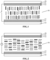
- an exemplary light-adjusting glass which includes a first substrate, a second substrate and a dye liquid crystal layer 30, wherein the first substrate and the second substrate are oppositely arranged, and the dye liquid crystal layer is arranged between the first substrate and the second substrate;
- the first substrate includes a first base 10, and a first electrode layer 11 and a first alignment layer 12 which are sequentially arranged on a side of the first base 10 proximal to the liquid crystal layer;
- the second substrate includes: a second base 20, and a second electrode layer 21 and a second alignment layer 22 which are sequentially arranged on a side of the second base 20 proximal to the liquid crystal layer;
- a material of the liquid crystal layer 30 includes liquid crystal molecules and dichroic dye molecules. Depending on dichroic properties of the dichroic dye molecules, only light in an incident light that is parallel to a long axis of the dye molecules may be absorbed.
- the light-adjusting glass is a TN-type liquid crystal cell, that is, a display mode thereof is a normally white mode.
- a display mode thereof is a normally white mode.
- the light-adjusting glass is in a bright state, as shown in FIG. 1 ; when a voltage is applied to the first electrode layer 11 and the second electrode layer 21, the light-adjusting glass is in a dark state, as shown in FIG. 2 .
- applying a voltage to the first electrode layer 11 and the second electrode layer 21 of the light-adjusting glass mainly includes two ways of: providing pads in peripheral regions of the first base 10 and the second base 20, exposing the pads, and welding the pads with leads, respectively, so that a size of the light-adjusting glass is inevitably increased by providing the pad regions in the peripheral regions of the first base and the second base; providing pads at a location corresponding to half of the peripheral region of the first base 10, and cutting off the other half of the peripheral region; providing the pads at the positions of the peripheral region of the second base 20 corresponding to the positions where the first base 10 is cut, cutting the other half of the peripheral region, and then welding the pads with leads, respectively.
- a size of the light-adjusting glass may be reduced compared to the first way, the second way needs an additional cutting process.
- a light-adjusting glass is provided in the following embodiments of the present disclosure.
- embodiments of the present disclosure provide a light-adjusting glass having an encapsulation region and a transmittance adjustment region defined by the encapsulation region; this light-adjusting glass includes: a first substrate, a second substrate, a dye liquid crystal layer 30 and a frame sealant 16, wherein the first substrate and the second substrate are provided oppositely, the dye liquid crystal layer is provided between the first substrate and the second substrate and is positioned in the transmittance adjustment region, and the frame sealant 16 is positioned in the encapsulation region; wherein, the first substrate includes: a first base 10, the first electrode layer 11 is arranged on a side of the first base 10 proximal to a dye liquid crystal layer; the second substrate includes: a second base 20, and a second electrode layer 21 disposed on a side of the second base 20 proximal to the dye liquid crystal layer.
- a conductive structure is disposed in the frame sealant 16; a first voltage transmission structure 14 and a second voltage transmission structure 13 electrically insulated from each other are further provided on the first base 10; the first voltage transmission structure 14 is connected to the first electrode layer 11; the second voltage transmission structure 13 is electrically connected to the second electrode layer 21 through the conductive structure in the frame sealant 16.
- a voltage may be applied to the first electrode layer 11 through the first voltage transmission structure 14, and a voltage may be applied to the second electrode layer 21 through the second voltage transmission structure 13, so that the liquid crystal molecules and the dye molecules in the dye liquid crystal layer sandwiched between the first electrode layer 11 and the second electrode layer 21 are rotated to adjust the transmittance of the light irradiated to the light-adjusting glass.
- the frame sealant 16 at least covers a portion of the second voltage transmission structure so that the conductive structure in the frame sealant 16 serves as a conductive medium between the second voltage transmission structure and the second electrode layer 21, and the second electrode layer 21 is powered by the second voltage transmission structure.
- the conductive structure in the frame sealant 16 includes, but is not limited to, a conductive gold ball formed in the frame sealant 16 in a doped manner. Conductive gold balls may be doped at each position of the frame sealant 16, or only the position corresponding to the second voltage transmission structure 13. It should be understood that, in order to prevent the first electrode layer 11 and the second electrode layer 21 from being electrically connected, the frame sealant 16 is disposed in an insulating manner from the first electrode layer 11.
- the light-adjusting glass includes: a first substrate, a second substrate, a dye liquid crystal layer and a frame sealant 16, wherein the first substrate and the second substrate are provided oppositely; the dye liquid crystal layer and the frame sealant 16 are provided between the first substrate and the second substrate; wherein the first substrate includes a first base 10, and a second voltage transmission structure 13, a first electrode layer 11 and a first voltage transmission structure 14 in a same layer, and an interlayer insulating layer 15 sequentially arranged on a side of the first base 10 distal to the dye liquid crystal layer.
- the second substrate includes a second base 20, and a second electrode layer 21 disposed on a side of the second base 20 proximal to the dye liquid crystal layer.
- the first electrode layer 11 and the second electrode layer 21 each include a plate-shaped electrode.
- the frame sealant 16 is disposed in the encapsulation region, specifically, may be disposed on the first base 10, or may be disposed on the second base 20. In this embodiment, the frame sealant 16 is disposed on the first base 10, the second voltage transmission structure 13 at least contacts with a position where a conductive structure is provided in the frame sealant 16.
- the first voltage transmission structure 14 and the first electrode layer 11 are formed as a single piece. That is, as shown in FIG. 1 , the first voltage transmission structure 14 and the first electrode layer 11 are integrally formed as a single piece, so that the first voltage transmission structure 14 and the first electrode layer 11 may be formed by a single patterning process.
- a material of the first electrode layer 11 includes, but is not limited to, Indium Tin Oxide (ITO).
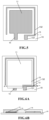
- the second voltage transmission structure 13 may be made of a metal conductive material, such as copper (C u ). Since the second electrode layer 21 is a plate-shaped electrode, in order to ensure that the voltage applied on the second electrode layer 21 is uniform, at this time, the second voltage transmission structure 13 is designed as a structure composed of a first transmission sub-structure 131 and a second transmission sub-structure 132, as shown in FIG. 4 ; wherein, the first transmission sub-structure 131 and the first voltage transmission structure 14 are located at the same side of the encapsulation region, as shown in FIG.
- a metal conductive material such as copper (C u ).
- the second transmission sub-structure 132 is located at the other sides of the encapsulation region except the side where the first transmission sub-structure 131 is located, that is, the second transmission sub-structure 132 is a U-shaped structure shown in FIG. 4 , and the first transmission sub-structure 131 is electrically connected to the second transmission sub-structure 132.
- the interlayer insulating layer 15 is hollowed at the positions where the first transmission sub-structure and the second transmission sub-structure are located, the first transmission sub-structure and the second transmission sub-structure are exposed, and the frame sealant 16 is provided in the encapsulation region and covers the first transmission sub-structure and the second transmission sub-structure.
- the second electrode layer 21 may be electrically connected to the first transmission sub-structure and the second transmission sub-structure through the conductive structure in the frame sealant 16.
- the embodiment of the present disclosure provides a method for manufacturing the light-adjusting glass.
- the encapsulation region is a rectangular closed loop structure having a first side and a second side which are oppositely disposed (opposite to each other in the left-right direction in FIG. 3 ), and a third side and a fourth side which are oppositely disposed (opposite to each other in the up-down direction in FIG. 3 ).
- the method includes steps of forming a first substrate, a second substrate, and a dye liquid crystal layer filled between the first substrate and the second substrate.
- the step of forming the first substrate includes the following steps:
- the first substrate has been manufactured.
- the step of forming the second substrate includes the following steps: Step 1, as shown in FIG. 11 , a pattern including the second electrode layer 21 is formed on the second base 20 through a patterning process; the second electrode layer 21 is sized to cover the transmittance adjustment region and the encapsulation region (corresponding to the region where the frame sealant 16 is located) when the second electrode layer 21 is assembled with the first substrate to form the light-adjusting glass, and at least a portion of the block-shaped structures of the first voltage transmission structures 14 and the second voltage transmission structures 13 is exposed by an orthographic projection of the second electrode layer 21 on the first base 10, so as to solder the leads onto the block-shaped structures of the first voltage transmission structures 14 and the second voltage transmission structures 13, so as to apply an external voltage to the first electrode layer 11 and the second electrode layer 21.
- the material of the second electrode layer 21 includes, but is not limited to, ITO.
- an insulating layer may be formed on the second base 20 to prevent the second base 20 from being damaged when the second electrode layer 21 is etched.
- the frame sealant 16 may also be formed on the second substrate, as long as the frame sealant 16 bonds the first and second substrates together. Thus, the second substrate has been manufactured.
- the structure of the light-adjusting glass is similar to that of the light-adjusting glass described above, except that the first electrode layer 11 includes a plurality of strip-shaped electrodes. In this way, different voltages are applied to the strip-shaped electrodes, such that rotation angles of liquid crystal molecules in the dye liquid crystal layer corresponding to different positions of the light-adjusting glass are different, thereby implementing a louver function.
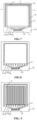
- the first voltage transmission structure 14 includes a plurality of first pads 141 and a plurality of second pads 142 that are disposed in one-to-one correspondence with the plurality of strip-shaped electrodes; the plurality of first pads 141 may be arranged side by side, a first end of each first pad 141 is connected to the corresponding strip-shaped electrode, a second end of each first pad 141 is connected to a first end of the corresponding second pad 142 through a fan-out trace 143 located in a fan-out region, and a second end of each second pad 142 is used for bonding to a chip IC to provide a voltage to the strip-shaped electrode.
- the second voltage transmission structure 13 may adopt the same structure as described above.
- the first transmission sub-structure of the second voltage transmission structure 13 may also adopt a third pad 133 disposed side by side with the second pads 142, where the third pad 133 is connected with the second transmission sub-structure through the fan-out trace 143.
- the first voltage transmission structure 14 and the second voltage transmission structure 13 are disposed in a same layer and have the same material. That is, the first pads 141 and the second pads 142 in the first voltage transmission structure 14 and the first transmission sub-structure and the second transmission sub-structure in the second voltage transmission structure 13 are manufactured by a single patterning process, and the material includes, but is not limited to, a conductive metal.
- a transition layer may also be disposed on the second ends of the second pads 142 for better bonding of the second pads 142 with the chip IC.
- the material of the transition layer includes, but is not limited to, ITO.
- the transition layer may be disposed in a same layer as the strip-shaped electrodes, that is, manufactured by a single patterning process.
- the embodiment of the present disclosure provides a method for manufacturing the light-adjusting glass.
- the light-adjusting glass is a rectangular glass
- the encapsulation region is a rectangular closed loop structure having a first side a and a second side b which are oppositely disposed (opposite to each other in the left-right direction in FIG. 7 ), and a third side c and a fourth side d which are oppositely disposed (opposite to each other in the up-down direction in FIG. 7 ).
- the method includes steps of forming a first substrate, a second substrate, and a dye liquid crystal layer filled between the first substrate and the second substrate.
- the formation of the second substrate and the dye liquid crystal layer is the same as the above steps and will not be described again.
- the step of forming the first substrate includes the following steps:
- the present disclosure provides a smart vehicle window, which includes the above light-adjusting glass.
- the smart vehicle window may be applied to an airplane, a building, and the like.
Landscapes
- Physics & Mathematics (AREA)
- Nonlinear Science (AREA)
- Mathematical Physics (AREA)
- Chemical & Material Sciences (AREA)
- Crystallography & Structural Chemistry (AREA)
- General Physics & Mathematics (AREA)
- Optics & Photonics (AREA)
- Geometry (AREA)
- Engineering & Computer Science (AREA)
- Mechanical Engineering (AREA)
- Liquid Crystal (AREA)
Claims (15)
- Verre de réglage de la lumière, comportant une zone de réglage de la transmission et une région d'encapsulation entourant au moins partiellement la région de réglage de la transmission ; le verre de réglage de la lumière comprend : un premier substrat et un deuxième substrat opposés l'un à l'autre, et une couche de cristaux liquides colorants (30) entre le premier substrat et le deuxième substrat dans la région de réglage de la transmission, et un scellant de cadre (16) dans la région d'encapsulation ; dans lequel le premier substrat comprend une première base (10) et une première couche d'électrodes (11) sur une face de la première base (10) proche de la couche de cristaux liquides colorants (30) ; le deuxième substrat comprend une deuxième base (20) et une deuxième couche d'électrodes (21) sur un côté de la deuxième base (20) à proximité de la couche de cristaux liquides colorants (30); caractérisé par le fait queune structure conductrice est prévue dans le scellant du cadre (16) ;une première structure de transmission de tension (14) et une deuxième structure de transmission de tension (13) isolés électriquement l'une de l'autre se trouvent sur la première base (10) ;la première structure de transmission de tension (14) est connectée électriquement à la première couche d'électrode (11) ; etle scellant du cadre (16) recouvre au moins une partie de la deuxième structure de transmission de tension (13), de sorte que la deuxième structure de transmission de tension (13) soit connectée électriquement à la deuxième couche d'électrodes (21) par l'intermédiaire de la structure conductrice dans le scellant du cadre (16),où la deuxième structure de transmission de tension (13) comprend : une première sous-structure de transmission (131) et une deuxième sous-structure de transmission (132) ;la première sous-structure de transmission (131) et la première structure de transmission de tension (14) se trouvent sur un même côté de la région d'encapsulation ; etla deuxième sous-structure de transmission (132) se trouve sur les autres côtés de la région d'encapsulation, à l'exception du côté pourvu de la première sous-structure de transmission (131) ; et est en forme de U et est positionnée sur un premier côté, un deuxième côté et un troisième côté de la région d'encapsulation ; la première sous-structure de transmission (131) est positionnée sur un quatrième côté de la région d'encapsulation ; et la première sous-structure de transmission (131) est connectée électriquement à la deuxième sous-structure de transmission (132) ; etune extrémité de la première sous-structure de transmission (131) est une structure en forme de bloc, et l'autre extrémité de la première sous-structure de transmission (131) et la deuxième sous-structure de transmission (131) sont formées d'une seule pièce.
- Verre de réglage de la lumière selon la revendication 1, dans lequel la deuxième structure de transmission de tension (13) se trouve dans une zone périphérique de la première couche d'électrodes (11) en entourant au moins partiellement la première couche d'électrode (11).
- Verre de réglage de la lumière selon la revendication 1 ou 2, dans lequel la première couche d'électrodes (11) et la deuxième couche d'électrodes (21) comprennent toutes deux des électrodes en forme de plaque.
- Verre de réglage de la lumière selon la revendication 3, dans lequel la première structure de transmission de tension (14) et la première couche d'électrodes (11) sont formées d'une seule pièce.
- Verre de réglage de la lumière selon la revendication 1 ou 2, dans lequel la première couche d'électrodes (11) comprend une pluralité d'électrodes en forme de bandes ; et la deuxième couche d'électrodes (21) comprend une électrode en forme de plaque.
- Verre de réglage de la lumière selon la revendication 5, dans lequel la première structure de transmission de tension (14) comprend une pluralité de premiers plots (141) et une pluralité de deuxièmes plots (142) ;les premières extrémités de la pluralité de premiers plots (141) proches de la première couche d'électrodes (11) sont couplées à la pluralité d'électrodes en forme de bande, respectivement ;les deuxièmes extrémités de la pluralité de premiers plots (141) distantes de la première couche d'électrodes (11) sont couplées électriquement aux premières extrémités de la pluralité de deuxièmes plots (142) proches de la première couche d'électrodes (11), par l'intermédiaire d'une pluralité de pistes en éventail (143), respectivement,de préférence, la pluralité de deuxièmes plots (142) se trouve sur la première base (10) à l'extérieur de la zone d'encapsulation.
- Verre de réglage de la lumière selon la revendication 6, dans lequel la pluralité de premiers plots (141) et la deuxième pluralité de plots se trouve dans une même couche et sont constituée d'un même matériau que la deuxième structure de transmission de tension (13) ; ou bien
le verre de réglage de la luminosité comprend en outre une couche de transition située à une deuxième extrémité de chacun des plots (142) de la deuxième pluralité distants de la première couche d'électrodes (11), et la couche de transition se trouve dans une même couche et est constituée d'un même matériau que les électrodes en forme de bande. - Verre de réglage de la lumière selon l'une des revendications 6 à 7, dans lequel l'extrémité de la première sous-structure de transmission (131) est un troisième plot relié électriquement à la deuxième sous-structure de transmission (132) par une piste de connexion ;le troisième plot et la pluralité de deuxièmes plots (142) sont disposés côte à côte ; etla piste de connexion et les pistes de sortie en éventail (143) sont disposées côte à côte.
- Verre de réglage de la lumière selon la revendication 7, dans lequel une projection orthographique de la deuxième couche d'électrodes (21) sur la première base (10) recouvre une projection orthographique de la première sous-structure de transmission (131) sur la première base (10).
- Verre de réglage de la lumière selon l'une des revendications 8 à 9, comprenant en outre une couche isolante intercalaire, dans laquelle la couche isolante intercalaire recouvre au moins la première couche d'électrodes (11) et expose la première sous-structure de transmission (131) et la deuxième sous-structure de transmission (132).
- Fenêtre de véhicule intelligente, comprenant le verre de réglage de la lumière de l'une des revendications 1 à 10.
- Méthode de fabrication d'un verre de réglage de la lumière, comprenant :former un premier substrat, comprenant : préparer une première base (10) et former une première couche d'électrodes (11), une première structure de transmission de tension (14) et une deuxième structure de transmission de tension (13) sur le premier substrat, où la première structure de transmission de tension (14) et la deuxième structure de transmission de tension (13) sont isolées électriquement l'une de l'autre ; la première couche d'électrodes (11) est pourvue d'une région de réglage de la transmission, et au moins une partie de la deuxième structure de transmission de tension (13) est pourvue d'une région de région d'encapsulation entourant au moins partiellement la région de réglage de la transmission ;former un scellant de cadre (16) dans la région d'encapsulation de telle sorte que le scellant de cadre (16) comprend une structure conductrice et une première partie qui recouvre au moins partiellement la deuxième structure de transmission de tension (13) ;former un deuxième substrat de sorte que le deuxième substrat comprend une deuxième base (20) et une deuxième couche d'électrodes (21) formée sur la deuxième base (20) ; etaligner et assembler le premier substrat et le deuxième substrat de manière à ce que le scellant de cadre (16) soit disposé entre le premier substrat et le deuxième substrat et qu'il soit lié à la deuxième couche d'électrode (21) ,où la deuxième structure de transmission de tension (13) comprend : une première sous-structure de transmission (131) et une deuxième sous-structure de transmission (132) ;la première sous-structure de transmission (131) et la première structure de transmission de tension (14) se trouvent du même côté de la région d'encapsulation ; etla deuxième sous-structure de transmission (132) se trouve sur les autres côtés de la région d'encapsulation, à l'exception du côté pourvu de la première sous-structure de transmission (131), et est en forme de U et est positionnée sur un premier côté, un deuxième côté et un troisième côté de la région d'encapsulation ; la première sous-structure de transmission (131) est positionnée sur un quatrième côté de la région d'encapsulation ; et la première sous-structure de transmission (131) est connectée électriquement à la deuxième sous-structure de transmission (132) ; etUne extrémité de la première sous-structure de transmission (131) est une structure en forme de bloc, et l'autre extrémité de la première sous-structure de transmission (131) et la deuxième sous-structure de transmission (132) sont formés d'une seule pièce.
- Méthode de fabrication d'un verre de réglage de la lumière selon la revendication 12, comprenant en outre la formation d'une couche isolante intercalaire sur la première couche d'électrodes (11) pour couvrir la première couche d'électrodes (11) et exposer la deuxième structure de transmission de tension (13), avant de former le scellant du cadre (16) dans la région d'encapsulation.
- Méthode de fabrication d'un verre de réglage de lumière selon la revendication 12 ou 13, dans laquelle la formation de la première couche d'électrodes (11) et de la première structure de transmission de tension (14) comprend la formation de la première couche d'électrodes (11) et de la première structure de transmission de tension (14) en une seule pièce par un seul procédé de façonnage avec un même matériau ; ou bien
dans laquelle la formation de la première couche d'électrodes (11) et de la première structure de transmission de tension (14) comprend la formation de la première couche d'électrodes (11) comprenant une pluralité d'électrodes en forme de bande et la première structure de transmission de tension (14) comprenant une pluralité de premiers plots (141) et une pluralité de deuxièmes plots (142), de sorte que les premières extrémités de la pluralité de premiers plots (141) à proximité de la première couche d'électrodes (11) sont connectées à la pluralité d'électrodes en forme de bande, respectivement ; les deuxièmes extrémités de la pluralité de premiers plots (141) distantes de la première couche d'électrodes (11) sont connectées électriquement aux premières extrémités de la pluralité de deuxièmes plots (142) proches de la première couche d'électrodes (11) par l'intermédiaire d'une pluralité de pistes en éventail (143), respectivement. - Méthode de fabrication d'un verre de réglage de la lumière selon la revendication 14, dans laquelle la formation des première et deuxième structures de transmission de tension (13, 14) comprend la formation de la pluralité des premiers plots (141), la pluralité de deuxièmes plots (142) et la deuxième structure de transmission de tension (13) par un seul processus de façonnage avec un même matériau, ou bien
dans laquelle la formation des première et deuxième structures de transmission de tension (13, 14) comprend la formation d'une couche de transition et la pluralité d'électrodes en forme de bande par un processus de façonnage unique avec un même matériau de sorte que la couche de transition soit disposée à une deuxième extrémité de chacune de la pluralité de deuxièmes électrodes (142) distantes de la première couche d'électrodes (11).
Applications Claiming Priority (2)
| Application Number | Priority Date | Filing Date | Title |
|---|---|---|---|
| CN201911271293.6A CN112987417B (zh) | 2019-12-12 | 2019-12-12 | 调光玻璃及智能车窗 |
| PCT/CN2020/134516 WO2021115253A1 (fr) | 2019-12-12 | 2020-12-08 | Verre commutable et fenêtre de véhicule intelligent |
Publications (3)
| Publication Number | Publication Date |
|---|---|
| EP4075191A1 EP4075191A1 (fr) | 2022-10-19 |
| EP4075191A4 EP4075191A4 (fr) | 2023-01-18 |
| EP4075191B1 true EP4075191B1 (fr) | 2025-06-18 |
Family
ID=76329559
Family Applications (1)
| Application Number | Title | Priority Date | Filing Date |
|---|---|---|---|
| EP20864335.3A Active EP4075191B1 (fr) | 2019-12-12 | 2020-12-08 | Verre commutable et fenêtre de véhicule intelligent |
Country Status (4)
| Country | Link |
|---|---|
| US (1) | US11598996B2 (fr) |
| EP (1) | EP4075191B1 (fr) |
| CN (1) | CN112987417B (fr) |
| WO (1) | WO2021115253A1 (fr) |
Families Citing this family (4)
| Publication number | Priority date | Publication date | Assignee | Title |
|---|---|---|---|---|
| CN114002871B (zh) * | 2020-07-27 | 2023-01-31 | 京东方科技集团股份有限公司 | 调光玻璃窗总成 |
| TWI793977B (zh) * | 2022-01-17 | 2023-02-21 | 絢麗光電股份有限公司 | 調光玻璃切換方法 |
| DE102023111079B4 (de) * | 2023-04-28 | 2025-02-13 | Webasto SE | Funktionsschicht-Rohling und Verfahren zum Kontaktieren eines Funktionsschicht-Rohlings |
| CN118244530B (zh) * | 2024-05-23 | 2024-09-10 | 惠科股份有限公司 | 显示装置及其制作方法 |
Family Cites Families (11)
| Publication number | Priority date | Publication date | Assignee | Title |
|---|---|---|---|---|
| JP2006106077A (ja) * | 2004-09-30 | 2006-04-20 | Seiko Epson Corp | 電気光学装置及び電子機器 |
| US20120044445A1 (en) * | 2010-08-17 | 2012-02-23 | Semiconductor Energy Laboratory Co., Ltd. | Liquid Crystal Device and Manufacturing Method Thereof |
| CN103135291B (zh) * | 2011-12-05 | 2015-09-16 | 上海天马微电子有限公司 | 一种3d液晶光栅装置及3d液晶显示装置 |
| JP6508656B2 (ja) | 2014-03-18 | 2019-05-08 | Tianma Japan株式会社 | 調光素子及びスマートガラス |
| EP4386475A3 (fr) * | 2015-11-13 | 2024-09-18 | Dai Nippon Printing Co., Ltd. | Film de commande de lumière et verre feuilleté |
| JP6716323B2 (ja) * | 2016-04-01 | 2020-07-01 | 株式会社ジャパンディスプレイ | 表示装置 |
| WO2017175796A1 (fr) * | 2016-04-05 | 2017-10-12 | 凸版印刷株式会社 | Module de gradation de lumière |
| CN107703663A (zh) * | 2017-09-26 | 2018-02-16 | 张家港康得新光电材料有限公司 | 2d/3d可切换面板及显示装置 |
| JP7062912B2 (ja) * | 2017-10-11 | 2022-05-09 | 大日本印刷株式会社 | 調光フィルム、調光部材、車両、調光システム及び調光フィルムの駆動方法 |
| CN209674156U (zh) * | 2019-05-24 | 2019-11-22 | 京东方科技集团股份有限公司 | 调光玻璃 |
| CN210803935U (zh) * | 2019-12-12 | 2020-06-19 | 京东方科技集团股份有限公司 | 调光玻璃及智能车窗 |
-
2019
- 2019-12-12 CN CN201911271293.6A patent/CN112987417B/zh active Active
-
2020
- 2020-12-08 EP EP20864335.3A patent/EP4075191B1/fr active Active
- 2020-12-08 WO PCT/CN2020/134516 patent/WO2021115253A1/fr not_active Ceased
- 2020-12-08 US US17/280,901 patent/US11598996B2/en active Active
Also Published As
| Publication number | Publication date |
|---|---|
| WO2021115253A1 (fr) | 2021-06-17 |
| EP4075191A4 (fr) | 2023-01-18 |
| EP4075191A1 (fr) | 2022-10-19 |
| CN112987417B (zh) | 2025-07-11 |
| CN112987417A (zh) | 2021-06-18 |
| US11598996B2 (en) | 2023-03-07 |
| US20220100021A1 (en) | 2022-03-31 |
Similar Documents
| Publication | Publication Date | Title |
|---|---|---|
| EP4075191A1 (fr) | Verre commutable et fenêtre de véhicule intelligent | |
| US11543719B2 (en) | Light control unit | |
| KR102108830B1 (ko) | 전기변색 디바이스 | |
| CN100380212C (zh) | 调光体及夹层玻璃 | |
| CN210803935U (zh) | 调光玻璃及智能车窗 | |
| KR20150031917A (ko) | 전극 플레이트와 이를 이용하는 전기변색 플레이트, 전기변색 미러 및 디스플레이 장치 | |
| EP1251391B1 (fr) | Dispositif électro-optique, son procédé de fabrication, et appareil électronique | |
| US7372534B2 (en) | Light adjuster with electrically conductive tape stuck on electrically conductive cylindrical housing in which is accommodated part of wiring | |
| JP7119305B2 (ja) | 調光体 | |
| JP7151137B2 (ja) | 調光ユニット | |
| EP4095594A1 (fr) | Panneau de gradation et son procédé de fabrication | |
| US20230121640A1 (en) | Laminated glazing with electrically connected layer and method of preparing a laminated glazing | |
| CN113711118B (zh) | 调光片以及调光装置 | |
| KR100856151B1 (ko) | 고분자 분산형 액정표시장치의 전극 단자부 제조방법 | |
| JP7254436B2 (ja) | 調光装置及び構造体 | |
| KR101153299B1 (ko) | 액정표시소자 및 그 제조방법 | |
| CN115421326B (zh) | 显示面板及其制备方法 | |
| JP2021076640A (ja) | 調光シートおよびその製造方法 | |
| WO2022222129A1 (fr) | Fenêtre de gradation et son procédé de fabrication | |
| US12326625B2 (en) | Tiled light transmitting controller | |
| US20260072317A1 (en) | Light control sheet and method of producing a light control sheet | |
| US20250389983A1 (en) | Cholesteric liquid crystal display device and manufacturing method thereof | |
| KR100348994B1 (ko) | 인 플레인 스위칭 모드의 액정 표시장치 제조방법 및 그 제조방법에 따른 액정표시장치 | |
| CN118011693A (zh) | 一种光电器件及应用其的可切换窗口、玻璃窗 | |
| JP2025171517A (ja) | 調光装置及び調光モジュール |
Legal Events
| Date | Code | Title | Description |
|---|---|---|---|
| STAA | Information on the status of an ep patent application or granted ep patent |
Free format text: STATUS: UNKNOWN |
|
| STAA | Information on the status of an ep patent application or granted ep patent |
Free format text: STATUS: THE INTERNATIONAL PUBLICATION HAS BEEN MADE |
|
| PUAI | Public reference made under article 153(3) epc to a published international application that has entered the european phase |
Free format text: ORIGINAL CODE: 0009012 |
|
| STAA | Information on the status of an ep patent application or granted ep patent |
Free format text: STATUS: REQUEST FOR EXAMINATION WAS MADE |
|
| 17P | Request for examination filed |
Effective date: 20210326 |
|
| AK | Designated contracting states |
Kind code of ref document: A1 Designated state(s): AL AT BE BG CH CY CZ DE DK EE ES FI FR GB GR HR HU IE IS IT LI LT LU LV MC MK MT NL NO PL PT RO RS SE SI SK SM TR |
|
| A4 | Supplementary search report drawn up and despatched |
Effective date: 20221216 |
|
| RIC1 | Information provided on ipc code assigned before grant |
Ipc: G02F 1/137 20060101ALI20221212BHEP Ipc: G02F 1/1343 20060101ALI20221212BHEP Ipc: G02F 1/1345 20060101AFI20221212BHEP |
|
| DAV | Request for validation of the european patent (deleted) | ||
| DAX | Request for extension of the european patent (deleted) | ||
| STAA | Information on the status of an ep patent application or granted ep patent |
Free format text: STATUS: EXAMINATION IS IN PROGRESS |
|
| 17Q | First examination report despatched |
Effective date: 20240223 |
|
| GRAP | Despatch of communication of intention to grant a patent |
Free format text: ORIGINAL CODE: EPIDOSNIGR1 |
|
| STAA | Information on the status of an ep patent application or granted ep patent |
Free format text: STATUS: GRANT OF PATENT IS INTENDED |
|
| RIC1 | Information provided on ipc code assigned before grant |
Ipc: B60J 3/04 20060101ALN20250115BHEP Ipc: G02F 1/1339 20060101ALN20250115BHEP Ipc: G02F 1/137 20060101ALI20250115BHEP Ipc: G02F 1/1343 20060101ALI20250115BHEP Ipc: G02F 1/1345 20060101AFI20250115BHEP |
|
| INTG | Intention to grant announced |
Effective date: 20250207 |
|
| GRAS | Grant fee paid |
Free format text: ORIGINAL CODE: EPIDOSNIGR3 |
|
| GRAA | (expected) grant |
Free format text: ORIGINAL CODE: 0009210 |
|
| STAA | Information on the status of an ep patent application or granted ep patent |
Free format text: STATUS: THE PATENT HAS BEEN GRANTED |
|
| AK | Designated contracting states |
Kind code of ref document: B1 Designated state(s): AL AT BE BG CH CY CZ DE DK EE ES FI FR GB GR HR HU IE IS IT LI LT LU LV MC MK MT NL NO PL PT RO RS SE SI SK SM TR |
|
| REG | Reference to a national code |
Ref country code: GB Ref legal event code: FG4D |
|
| REG | Reference to a national code |
Ref country code: CH Ref legal event code: EP |
|
| REG | Reference to a national code |
Ref country code: DE Ref legal event code: R096 Ref document number: 602020053054 Country of ref document: DE |
|
| REG | Reference to a national code |
Ref country code: CH Ref legal event code: EP |
|
| REG | Reference to a national code |
Ref country code: IE Ref legal event code: FG4D |
|
| PG25 | Lapsed in a contracting state [announced via postgrant information from national office to epo] |
Ref country code: FI Free format text: LAPSE BECAUSE OF FAILURE TO SUBMIT A TRANSLATION OF THE DESCRIPTION OR TO PAY THE FEE WITHIN THE PRESCRIBED TIME-LIMIT Effective date: 20250618 |
|
| REG | Reference to a national code |
Ref country code: LT Ref legal event code: MG9D |
|
| PG25 | Lapsed in a contracting state [announced via postgrant information from national office to epo] |
Ref country code: NO Free format text: LAPSE BECAUSE OF FAILURE TO SUBMIT A TRANSLATION OF THE DESCRIPTION OR TO PAY THE FEE WITHIN THE PRESCRIBED TIME-LIMIT Effective date: 20250918 Ref country code: GR Free format text: LAPSE BECAUSE OF FAILURE TO SUBMIT A TRANSLATION OF THE DESCRIPTION OR TO PAY THE FEE WITHIN THE PRESCRIBED TIME-LIMIT Effective date: 20250919 |
|
| PG25 | Lapsed in a contracting state [announced via postgrant information from national office to epo] |
Ref country code: BG Free format text: LAPSE BECAUSE OF FAILURE TO SUBMIT A TRANSLATION OF THE DESCRIPTION OR TO PAY THE FEE WITHIN THE PRESCRIBED TIME-LIMIT Effective date: 20250618 |
|
| PG25 | Lapsed in a contracting state [announced via postgrant information from national office to epo] |
Ref country code: HR Free format text: LAPSE BECAUSE OF FAILURE TO SUBMIT A TRANSLATION OF THE DESCRIPTION OR TO PAY THE FEE WITHIN THE PRESCRIBED TIME-LIMIT Effective date: 20250618 |
|
| PG25 | Lapsed in a contracting state [announced via postgrant information from national office to epo] |
Ref country code: RS Free format text: LAPSE BECAUSE OF FAILURE TO SUBMIT A TRANSLATION OF THE DESCRIPTION OR TO PAY THE FEE WITHIN THE PRESCRIBED TIME-LIMIT Effective date: 20250918 |
|
| REG | Reference to a national code |
Ref country code: NL Ref legal event code: MP Effective date: 20250618 |
|
| PG25 | Lapsed in a contracting state [announced via postgrant information from national office to epo] |
Ref country code: LV Free format text: LAPSE BECAUSE OF FAILURE TO SUBMIT A TRANSLATION OF THE DESCRIPTION OR TO PAY THE FEE WITHIN THE PRESCRIBED TIME-LIMIT Effective date: 20250618 |
|
| PG25 | Lapsed in a contracting state [announced via postgrant information from national office to epo] |
Ref country code: NL Free format text: LAPSE BECAUSE OF FAILURE TO SUBMIT A TRANSLATION OF THE DESCRIPTION OR TO PAY THE FEE WITHIN THE PRESCRIBED TIME-LIMIT Effective date: 20250618 |
|
| PG25 | Lapsed in a contracting state [announced via postgrant information from national office to epo] |
Ref country code: PT Free format text: LAPSE BECAUSE OF FAILURE TO SUBMIT A TRANSLATION OF THE DESCRIPTION OR TO PAY THE FEE WITHIN THE PRESCRIBED TIME-LIMIT Effective date: 20251020 |
|
| REG | Reference to a national code |
Ref country code: AT Ref legal event code: MK05 Ref document number: 1804731 Country of ref document: AT Kind code of ref document: T Effective date: 20250618 |
|
| PG25 | Lapsed in a contracting state [announced via postgrant information from national office to epo] |
Ref country code: IS Free format text: LAPSE BECAUSE OF FAILURE TO SUBMIT A TRANSLATION OF THE DESCRIPTION OR TO PAY THE FEE WITHIN THE PRESCRIBED TIME-LIMIT Effective date: 20251018 |
|
| PGFP | Annual fee paid to national office [announced via postgrant information from national office to epo] |
Ref country code: DE Payment date: 20251211 Year of fee payment: 6 |
|
| PGFP | Annual fee paid to national office [announced via postgrant information from national office to epo] |
Ref country code: GB Payment date: 20251219 Year of fee payment: 6 |
|
| PG25 | Lapsed in a contracting state [announced via postgrant information from national office to epo] |
Ref country code: AT Free format text: LAPSE BECAUSE OF FAILURE TO SUBMIT A TRANSLATION OF THE DESCRIPTION OR TO PAY THE FEE WITHIN THE PRESCRIBED TIME-LIMIT Effective date: 20250618 Ref country code: SM Free format text: LAPSE BECAUSE OF FAILURE TO SUBMIT A TRANSLATION OF THE DESCRIPTION OR TO PAY THE FEE WITHIN THE PRESCRIBED TIME-LIMIT Effective date: 20250618 |
|
| PG25 | Lapsed in a contracting state [announced via postgrant information from national office to epo] |
Ref country code: CZ Free format text: LAPSE BECAUSE OF FAILURE TO SUBMIT A TRANSLATION OF THE DESCRIPTION OR TO PAY THE FEE WITHIN THE PRESCRIBED TIME-LIMIT Effective date: 20250618 |
|
| PG25 | Lapsed in a contracting state [announced via postgrant information from national office to epo] |
Ref country code: PL Free format text: LAPSE BECAUSE OF FAILURE TO SUBMIT A TRANSLATION OF THE DESCRIPTION OR TO PAY THE FEE WITHIN THE PRESCRIBED TIME-LIMIT Effective date: 20250618 |
|
| PG25 | Lapsed in a contracting state [announced via postgrant information from national office to epo] |
Ref country code: EE Free format text: LAPSE BECAUSE OF FAILURE TO SUBMIT A TRANSLATION OF THE DESCRIPTION OR TO PAY THE FEE WITHIN THE PRESCRIBED TIME-LIMIT Effective date: 20250618 |
|
| PG25 | Lapsed in a contracting state [announced via postgrant information from national office to epo] |
Ref country code: SK Free format text: LAPSE BECAUSE OF FAILURE TO SUBMIT A TRANSLATION OF THE DESCRIPTION OR TO PAY THE FEE WITHIN THE PRESCRIBED TIME-LIMIT Effective date: 20250618 |
|
| PG25 | Lapsed in a contracting state [announced via postgrant information from national office to epo] |
Ref country code: ES Free format text: LAPSE BECAUSE OF FAILURE TO SUBMIT A TRANSLATION OF THE DESCRIPTION OR TO PAY THE FEE WITHIN THE PRESCRIBED TIME-LIMIT Effective date: 20250618 |
|
| PG25 | Lapsed in a contracting state [announced via postgrant information from national office to epo] |
Ref country code: RO Free format text: LAPSE BECAUSE OF FAILURE TO SUBMIT A TRANSLATION OF THE DESCRIPTION OR TO PAY THE FEE WITHIN THE PRESCRIBED TIME-LIMIT Effective date: 20250618 |
|
| REG | Reference to a national code |
Ref country code: DE Ref legal event code: R097 Ref document number: 602020053054 Country of ref document: DE |
|
| PG25 | Lapsed in a contracting state [announced via postgrant information from national office to epo] |
Ref country code: DK Free format text: LAPSE BECAUSE OF FAILURE TO SUBMIT A TRANSLATION OF THE DESCRIPTION OR TO PAY THE FEE WITHIN THE PRESCRIBED TIME-LIMIT Effective date: 20250618 |
|
| PG25 | Lapsed in a contracting state [announced via postgrant information from national office to epo] |
Ref country code: IT Free format text: LAPSE BECAUSE OF FAILURE TO SUBMIT A TRANSLATION OF THE DESCRIPTION OR TO PAY THE FEE WITHIN THE PRESCRIBED TIME-LIMIT Effective date: 20250618 |
|
| PLBE | No opposition filed within time limit |
Free format text: ORIGINAL CODE: 0009261 |
|
| STAA | Information on the status of an ep patent application or granted ep patent |
Free format text: STATUS: NO OPPOSITION FILED WITHIN TIME LIMIT |
|
| REG | Reference to a national code |
Ref country code: CH Ref legal event code: L10 Free format text: ST27 STATUS EVENT CODE: U-0-0-L10-L00 (AS PROVIDED BY THE NATIONAL OFFICE) Effective date: 20260430 |