EP4075596A1 - Antennenmodul, das schwimmende strahler in einem kommunikationssystem umfasst, und elektronische vorrichtung, die dasselbe umfasst - Google Patents
Antennenmodul, das schwimmende strahler in einem kommunikationssystem umfasst, und elektronische vorrichtung, die dasselbe umfasst Download PDFInfo
- Publication number
- EP4075596A1 EP4075596A1 EP21741861.5A EP21741861A EP4075596A1 EP 4075596 A1 EP4075596 A1 EP 4075596A1 EP 21741861 A EP21741861 A EP 21741861A EP 4075596 A1 EP4075596 A1 EP 4075596A1
- Authority
- EP
- European Patent Office
- Prior art keywords
- floating
- electronic device
- antenna
- radiator
- radiators
- Prior art date
- Legal status (The legal status is an assumption and is not a legal conclusion. Google has not performed a legal analysis and makes no representation as to the accuracy of the status listed.)
- Pending
Links
Images


Classifications
-
- H—ELECTRICITY
- H01—ELECTRIC ELEMENTS
- H01Q—ANTENNAS, i.e. RADIO AERIALS
- H01Q21/00—Antenna arrays or systems
- H01Q21/06—Arrays of individually energised antenna units similarly polarised and spaced apart
- H01Q21/061—Two dimensional planar arrays
- H01Q21/065—Patch antenna array
-
- H—ELECTRICITY
- H01—ELECTRIC ELEMENTS
- H01Q—ANTENNAS, i.e. RADIO AERIALS
- H01Q1/00—Details of, or arrangements associated with, antennas
- H01Q1/12—Supports; Mounting means
- H01Q1/22—Supports; Mounting means by structural association with other equipment or articles
- H01Q1/24—Supports; Mounting means by structural association with other equipment or articles with receiving set
- H01Q1/241—Supports; Mounting means by structural association with other equipment or articles with receiving set used in mobile communications, e.g. GSM
- H01Q1/246—Supports; Mounting means by structural association with other equipment or articles with receiving set used in mobile communications, e.g. GSM specially adapted for base stations
-
- H—ELECTRICITY
- H01—ELECTRIC ELEMENTS
- H01Q—ANTENNAS, i.e. RADIO AERIALS
- H01Q21/00—Antenna arrays or systems
- H01Q21/06—Arrays of individually energised antenna units similarly polarised and spaced apart
-
- H—ELECTRICITY
- H01—ELECTRIC ELEMENTS
- H01Q—ANTENNAS, i.e. RADIO AERIALS
- H01Q1/00—Details of, or arrangements associated with, antennas
- H01Q1/12—Supports; Mounting means
- H01Q1/22—Supports; Mounting means by structural association with other equipment or articles
- H01Q1/24—Supports; Mounting means by structural association with other equipment or articles with receiving set
-
- H—ELECTRICITY
- H01—ELECTRIC ELEMENTS
- H01Q—ANTENNAS, i.e. RADIO AERIALS
- H01Q1/00—Details of, or arrangements associated with, antennas
- H01Q1/36—Structural form of radiating elements, e.g. cone, spiral, umbrella; Particular materials used therewith
- H01Q1/38—Structural form of radiating elements, e.g. cone, spiral, umbrella; Particular materials used therewith formed by a conductive layer on an insulating support
-
- H—ELECTRICITY
- H01—ELECTRIC ELEMENTS
- H01Q—ANTENNAS, i.e. RADIO AERIALS
- H01Q1/00—Details of, or arrangements associated with, antennas
- H01Q1/52—Means for reducing coupling between antennas; Means for reducing coupling between an antenna and another structure
- H01Q1/521—Means for reducing coupling between antennas; Means for reducing coupling between an antenna and another structure reducing the coupling between adjacent antennas
- H01Q1/523—Means for reducing coupling between antennas; Means for reducing coupling between an antenna and another structure reducing the coupling between adjacent antennas between antennas of an array
-
- H—ELECTRICITY
- H01—ELECTRIC ELEMENTS
- H01Q—ANTENNAS, i.e. RADIO AERIALS
- H01Q15/00—Devices for reflection, refraction, diffraction or polarisation of waves radiated from an antenna, e.g. quasi-optical devices
- H01Q15/0006—Devices acting selectively as reflecting surface, as diffracting or as refracting device, e.g. frequency filtering or angular spatial filtering devices
- H01Q15/006—Selective devices having photonic band gap materials or materials of which the material properties are frequency dependent, e.g. perforated substrates, high-impedance surfaces
-
- H—ELECTRICITY
- H01—ELECTRIC ELEMENTS
- H01Q—ANTENNAS, i.e. RADIO AERIALS
- H01Q19/00—Combinations of primary active antenna elements and units with secondary devices, e.g. with quasi-optical devices, for giving the antenna a desired directional characteristic
- H01Q19/005—Patch antenna using one or more coplanar parasitic elements
-
- H—ELECTRICITY
- H01—ELECTRIC ELEMENTS
- H01Q—ANTENNAS, i.e. RADIO AERIALS
- H01Q5/00—Arrangements for simultaneous operation of antennas on two or more different wavebands, e.g. dual-band or multi-band arrangements
- H01Q5/30—Arrangements for providing operation on different wavebands
- H01Q5/378—Combination of fed elements with parasitic elements
- H01Q5/385—Two or more parasitic elements
-
- H—ELECTRICITY
- H01—ELECTRIC ELEMENTS
- H01Q—ANTENNAS, i.e. RADIO AERIALS
- H01Q5/00—Arrangements for simultaneous operation of antennas on two or more different wavebands, e.g. dual-band or multi-band arrangements
- H01Q5/30—Arrangements for providing operation on different wavebands
- H01Q5/378—Combination of fed elements with parasitic elements
- H01Q5/392—Combination of fed elements with parasitic elements the parasitic elements having dual-band or multi-band characteristics
-
- H—ELECTRICITY
- H01—ELECTRIC ELEMENTS
- H01Q—ANTENNAS, i.e. RADIO AERIALS
- H01Q9/00—Electrically-short antennas having dimensions not more than twice the operating wavelength and consisting of conductive active radiating elements
- H01Q9/04—Resonant antennas
- H01Q9/0407—Substantially flat resonant element parallel to ground plane, e.g. patch antenna
- H01Q9/0464—Annular ring patch
Definitions
- the disclosure relates to a communication system and, more specifically, to an antenna module including multiple floating radiators, and an electronic device including the same.
- the 5G or pre-5G communication system is also called a 'Beyond 4G Network' or a 'Post Long Term Evolution (LTE) System'.
- the 5G communication system is considered to be implemented in higher frequency (mmWave) bands, e.g., 60GHz bands, so as to accomplish higher data rates.
- the beamforming, massive multiple-input multiple-output (MIMO), Full Dimensional MIMO (FD-MIMO), array antenna, an analog beam forming, large scale antenna techniques are discussed in 5G communication systems.
- MIMO massive multiple-input multiple-output
- FD-MIMO Full Dimensional MIMO
- array antenna an analog beam forming, large scale antenna techniques.
- system network improvement is under way based on advanced small cells, cloud Radio Access Networks (RANs), ultra-dense networks, device-to-device (D2D) communication, wireless backhaul, moving network, cooperative communication, Coordinated Multi-Points (CoMP), reception-end interference cancellation and the like.
- RANs cloud Radio Access Networks
- D2D device-to-device
- CoMP Coordinated Multi-Points
- FSK Hybrid Frequency Shift Keying
- QAM Quadrature Amplitude Modulation
- SWSC sliding window superposition coding
- ACM advanced coding modulation
- FBMC filter bank multi carrier
- NOMA non-orthogonal multiple access
- SCMA sparse code multiple access
- the Internet which is a human centered connectivity network where humans generate and consume information
- IoT Internet of Things
- IoE Internet of Everything
- sensing technology “wired/wireless communication and network infrastructure”, “service interface technology”, and “Security technology”
- M2M Machine-to-Machine
- MTC Machine Type Communication
- IoT Internet technology services
- IoT may be applied to a variety of fields including smart home, smart building, smart city, smart car or connected cars, smart grid, health care, smart appliances and advanced medical services through convergence and combination between existing Information Technology (IT) and various industrial applications.
- IT Information Technology
- technologies such as a sensor network, Machine Type Communication (MTC), and Machine-to-Machine (M2M) communication may be implemented by beamforming, MIMO, and array antennas.
- MTC Machine Type Communication
- M2M Machine-to-Machine
- Application of a cloud Radio Access Network (RAN) as the above-described Big Data processing technology may also be considered to be as an example of convergence between the 5G technology and the IoT technology.
- RAN Radio Access Network
- the disclosure may provide an antenna module structure for improving the side ratio and rear ratio of an antenna module of an electronic device in a communication system.
- the disclosure may provide an antenna module structure for improving the directivity of a beam radiated from an antenna module.
- the disclosure may provide an antenna module structure having a wide aperture for improving the directivity of a beam radiated from an antenna module.
- the disclosure may provide an antenna module structure for reducing surface waves of electromagnetic waves radiated from an antenna module.
- An electronic device includes: a board; a plurality of antenna arrays arranged on the board; and a plurality of floating radiator arrays arranged to be spaced apart from the plurality of antenna arrays by a predetermined distance on the board.
- the plurality of floating radiator arrays are electromagnetically coupled to the plurality of antenna arrays.
- a first floating radiator array among the plurality of floating radiator arrays may be disposed to be spaced apart from a first side of a first antenna array among the plurality of antenna arrays by a predetermined distance.
- a second floating radiator array among the plurality of floating radiator arrays may be disposed to be spaced apart from a second side of the first antenna array among the plurality of antenna arrays by a predetermined distance.
- the second floating radiator array may be disposed to be spaced apart from a first side of a second antenna array among the plurality of antenna arrays by a predetermined distance.
- Each of the plurality of floating radiator arrays may include a plurality of floating radiators.
- Each of the plurality of floating radiators may have a ring shape.
- the ring shape may include at least one of a rectangular ring shape, a circular ring shape, and a diamond-shaped ring shape.
- Each of the plurality of floating radiators may include a capacitor and first to fourth inductors.
- a factor value of each of the capacitor and the first to fourth inductors may be determined according to at least one of a horizontal length, a vertical length, a thickness, and a line width of each of the plurality of floating radiators.
- a first end of the first inductor may be electrically connected to a second end of the fourth inductor.
- a second end of the first inductor may be electrically connected to a first end of the second inductor.
- a second end of the second inductor may be electrically connected to a first end of the third inductor.
- a third end of the second inductor may be electrically connected to a first end of the capacitor.
- a second end of the third inductor may be electrically connected to the second end of the fourth inductor.
- a third end of the fourth inductor may be electrically connected to a second end of the capacitor.
- Each of the plurality of floating radiators may be a patch-type radiator.
- the patch-type radiator may have at least one shape of a diamond shape and a rectangular patch shape.
- the electronic device may further include a feeding circuit configured to supply an electrical signal to the plurality of antenna arrays.
- the plurality of antenna arrays may radiate a first electromagnetic wave, based on the electrical signal.
- the plurality of floating radiator arrays may be electromagnetically coupled to the plurality of antenna arrays, based on the first electromagnetic wave, so as to radiate a second electromagnetic wave.
- a phase of the first electromagnetic wave may correspond to a phase of the second electromagnetic wave.
- the phase of the first electromagnetic wave and the phase of the second electromagnetic wave may be determined according to at least one of a horizontal length, a vertical length, a thickness, and a line width of each of the plurality of floating radiators.
- An electronic device may improve communication performance by improving the side ratio and rear ratio of an antenna module.
- An electronic device may improve the directivity of a beam radiated from an antenna module.
- An electronic device may improve the directivity of a beam radiated from an antenna module by increasing the area of an aperture for radiating beams through multiple floating radiators.
- An electronic device may reduce surface waves of electromagnetic waves radiated from an antenna module.
- the disclosure will be described using terms and names defined in the 5GS and NR standard, which is the latest standard specified by the 3rd generation partnership project (3GPP) group among the existing communication standards, for the convenience of description.
- 3GPP 3rd generation partnership project
- the disclosure is not limited by these terms and names, and may be applied in the same way to systems that conform other standards.
- the disclosure may be applied to 3GPP 5GS/NR (5th generation mobile communication standard).
- Fig. 1 is a block diagram illustrating an electronic device 10 in a network environment according to various embodiments.
- the electronic device 10 in the network environment may communicate with any other electronic device (not shown) or a server (not shown) via a network (e.g., a wired or wireless communication network).
- a network e.g., a wired or wireless communication network
- the electronic device 10 may be a base station and the other electronic device may be a terminal.
- the electronic device 10 may include an antenna module 11, a communication module 12, a processor 13, a memory 14, and an interface 15.
- at least one of the components may be omitted from the electronic device 10, or one or more other components may be added in the electronic device 10.
- some of the components may be integrated into a single element.
- the processor 13 may control, for example, at least one other component (e.g., a hardware or software component) of the electronic device 10, coupled with the processor 13, and may perform various data processing or computation. According to one embodiment, as at least part of the data processing or computation, the processor 13 may store a command or data received from another component (e.g., the communication module 12) in the memory 14, process the command or the data stored in the memory 14, and store resulting data in the memory 14.
- another component e.g., the communication module 12
- the memory 14 may store various data used by at least one component of the electronic device 10.
- the data may include, for example, software and input data or output data for a command related thereto.
- the interface 15 may support one or more specified protocols that may be used for the electronic device 10 to be coupled directly or wirelessly with any other electronic device.
- the interface 15 may include, for example, a universal serial bus (USB) interface or a secure digital (SD) card interface.
- USB universal serial bus
- SD secure digital
- the communication module 12 may support establishing a wired communication channel or a wireless communication channel between the electronic device 10 and any other electronic device and performing communication via the established communication channel.
- the communication module 12 may include one or more communication processors that are operable independently from the processor 13 and supports a wired communication or a wireless communication.
- the communication module 12 may communicate with any other electronic device or a server via a legacy cellular network, a 5G network, a next-generation communication network, the Internet, or a computer network (e.g., LAN or WAN).
- a legacy cellular network e.g., a single chip
- multi components e.g., multi chips
- the communication module 12 may supports 5G network and next-generation communication technologies beyond the 4G network, for example, new radio (NR) access technology.
- the NR access technology may support high-speed transmission of high-capacity data (enhanced mobile broadband (eMBB)), terminal power minimization and multi-terminal access (massive machine type communications (mMTC)), or ultra-reliable and low-latency communications (URLLC).
- eMBB enhanced mobile broadband
- mMTC massive machine type communications
- URLLC ultra-reliable and low-latency communications
- the communication module 12 may support ultrahigh frequency (mmWave) bands so as to accomplish higher data rates.
- the communication module 12 may support various techniques for ensuring performance in the ultrahigh frequency bands, such as beamforming, massive multiple-input multiple-output (massive MIMO), full dimensional MIMO (FD-MIMO), array antenna, analog beam forming, large scale antenna techniques.
- the communication module 12 support various requirements specified for the electronic device 10, any other electronic device, or a network system.
- the antenna module 11 may transmit or receive a signal or power to or from the outside (e.g., any other electronic device) of the electronic device 10.
- the antenna module 11 may include an antenna including a radiating element composed of a conductive material or a conductive pattern formed on a substrate (e.g., PCB).
- the antenna module 11 may include a plurality of antennas. In such a case, at least one antenna appropriate for a communication scheme used in a network may be selected, for example, by the communication module 12 from the plurality of antennas. The signal or the power may then be transmitted or received between the communication module 12 and any other external electronic device via the selected at least one antenna.
- another component e.g., a radio frequency integrated circuit (RFIC)
- RFIC radio frequency integrated circuit
- the antenna module 11 may form a mmWave antenna module.
- the mmWave antenna module may include a printed circuit board, a RFIC disposed at a first surface (e.g., the lower surface) of the printed circuit board or adjacent thereto and capable of supporting specified high-frequency bands (e.g., mmWave bands), and a plurality of antennas (e.g., an array antenna) disposed at a second surface (e.g., the upper or side surface) of the printed circuit board or adjacent thereto and capable of transmitting or receiving signals in the specified high-frequency bands.
- a RFIC disposed at a first surface (e.g., the lower surface) of the printed circuit board or adjacent thereto and capable of supporting specified high-frequency bands (e.g., mmWave bands)
- a plurality of antennas e.g., an array antenna
- At least some of the above-described components may be coupled mutually and communicate signals (e.g., commands or data) therebetween via an inter-peripheral communication scheme (e.g., a bus, general purpose input and output (GPIO), serial peripheral interface (SPI), or mobile industry processor interface (MIPI)).
- an inter-peripheral communication scheme e.g., a bus, general purpose input and output (GPIO), serial peripheral interface (SPI), or mobile industry processor interface (MIPI)
- commands or data may be transmitted or received between the electronic device 10 and any other external electronic device via a server coupled with a network.
- the other external electronic device may be a device of a same type as, or a different type, from the electronic device 10.
- all or some of operations to be executed at the electronic device 10 may be executed at the other external electronic device. For example, if the electronic device 10 should perform a function or a service automatically, or in response to a request from a user or another device, the electronic device 10, instead of, or in addition to, executing the function or the service, may request one or more other external electronic devices to perform at least part of the function or the service.
- the one or more other external electronic devices receiving the request may perform the at least part of the function or the service requested, or an additional function or an additional service related to the request, and transfer an outcome of the performing to the electronic device 10.
- the electronic device 10 may provide the outcome, with or without further processing of the outcome, as at least part of a reply to the request.
- a cloud computing, distributed computing, mobile edge computing (MEC), or client-server computing technology may be used, for example.
- the electronic device 10 may provide, for example, an ultra-low-latency service using distributed computing or MEC.
- the other external electronic devices may include Internet of things (IoT) devices.
- IoT Internet of things
- the electronic device according to various embodiments disclosed herein may be one of various types of electronic devices.
- the electronic device according to embodiments of the disclosure is not limited to those described above.
- each of such phrases as “A or B,” “at least one of A and B,” “at least one of A or B,” “A, B, or C,” “at least one of A, B, and C,” and “at least one of A, B, or C” may include all possible combinations of the items enumerated together in a corresponding one of the phrases.
- such terms as “a first”, “a second”, “the first”, and “the second” may be used to simply distinguish a corresponding element from another, and does not limit the elements in other aspect (e.g., importance or order).
- an element e.g., a first element
- the element may be coupled/connected with/to the other element directly (e.g., wiredly), wirelessly, or via a third element.
- module may include a unit implemented in hardware, software, or firmware, and may be interchangeably used with other terms, for example, “logic,” “logic block,” “component,” or “circuit”.
- the “module” may be a minimum unit of a single integrated component adapted to perform one or more functions, or a part thereof.
- the “module” may be implemented in the form of an application-specific integrated circuit (ASIC).
- ASIC application-specific integrated circuit
- Various embodiments as set forth herein may be implemented as software including one or more instructions that are stored in a storage medium (e.g., the memory 14) that is readable by a machine (e.g., the electronic device 10).
- a processor e.g., the processor 13
- the one or more instructions may include a code generated by a complier or a code executable by an interpreter.
- the machine-readable storage medium may be provided in the form of a non-transitory storage medium.
- non-transitory simply means that the storage medium is a tangible device, and does not include a signal (e.g., an electromagnetic wave), but this term does not differentiate between where data is semi-permanently stored in the storage medium and where the data is temporarily stored in the storage medium.
- a signal e.g., an electromagnetic wave
- a method may be included and provided in a computer program product.
- the computer program product may be traded as a product between a seller and a buyer.
- the computer program product may be distributed in the form of a machine-readable storage medium (e.g., compact disc read only memory (CD-ROM)), or be distributed (e.g., downloaded or uploaded) online via an application store (e.g., Play StoreTM), or between two user devices (e.g., smart phones) directly. If distributed online, at least part of the computer program product may be temporarily generated or at least temporarily stored in the machine-readable storage medium, such as memory of the manufacturer's server, a server of the application store, or a relay server.
- CD-ROM compact disc read only memory
- an application store e.g., Play StoreTM
- two user devices e.g., smart phones
- each element e.g., a module or a program of the above-described elements may include a single entity or multiple entities, and some of the multiple entities may be separately disposed in any other element.
- one or more of the above-described elements may be omitted, or one or more other elements may be added.
- a plurality of elements e.g., modules or programs
- the integrated element may still perform one or more functions of each of the plurality of elements in the same or similar manner as they are performed by a corresponding one of the plurality of elements before the integration.
- operations performed by the module, the program, or another element may be carried out sequentially, in parallel, repeatedly, or heuristically, or one or more of the operations may be executed in a different order or omitted, or one or more other operations may be added.
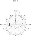
- FIG. 2 is a graph illustrating antenna gain of an antenna module 11 of an electronic device 10, according to various embodiments.
- a value 21 in a front direction and values 22 and 23 in a lateral direction may be different from each other.
- a side ratio of an antenna may be defined as a difference between an antenna gain value 21 with respect to the front direction and an antenna gain value 21 or 22 with respect to the lateral direction of the electromagnetic wave radiated from the antenna module 11.
- the antenna module 11 may include a plurality of antenna arrays.
- the influence on another antenna array positioned on a side surface of the one antenna array may be reduced.
- the mutual influence of the plurality of antenna arrays may be reduced.
- the antenna module 11 of the electronic device 10 may have a structure which reduces a side ratio.
- the structure of the antenna module 11 may be as shown in FIG. 3 .
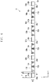
- FIG. 3 is a top view of the antenna module 11 of the electronic device 10, according to various embodiments.
- FIG. 4 is a side view of the antenna module 11 of the electronic device 10, according to various embodiments.
- the antenna module 11 may include a board 100, a plurality of antenna elements 110a to 140c, and a plurality of floating radiators 210a to 250c.
- the plurality of antenna elements 110a to 140c may be disposed on an upper surface of the board 100.
- First antenna elements 110a to 110c may be disposed in a first column of the board 100.
- a 1a-th antenna element 110a may be disposed in a first row of the first column of the board 100.
- the 1a-th antenna element 110a may include a 1a-th body 111a and a 1a-th supporter 112a.
- a 1b-th antenna element 110b may be disposed in a second row of the first column of the board 100.
- the 1b-th antenna element 110b may include a 1b-th body 111b and a 1b-th supporter 112b.
- a 1c-th antenna element 110c may be disposed in a third row of the first column of the board 100.
- the 1c-th antenna element 110c may include a 1c-th body 111c and a 1c-th supporter 112c.
- Second antenna elements 120a to 120c may be disposed in a second column of the board 100.
- a 2a-th antenna element 120a may be disposed in a first row of the second column of the board 100.
- the 2a-th antenna element 120a may include a 2a-th body 121a and a 2a-th supporter 122a.
- a 2b-th antenna element 120b may be disposed in a second row of the second column of the board 100.
- the 2b-th antenna element 120b may include a 2b-th body 121b and a 2b-th supporter 122b.
- a 2c-th antenna element 120c may be disposed in a third row of the second column of the board 100.
- the 2c-th antenna element 120c may include a 2c-th body 121c and a 2c-th supporter 122c.
- Third antenna elements 130a to 130c may be disposed in a third column of the board 100.
- a 3a-th antenna element 130a may be disposed in a first row of the third column of the board 100.
- the 3a-th antenna element 130a may include a 3a-th body 131a and a 3a-th supporter 132a.
- a 3b-th antenna element 130b may be disposed in a second row of the third column of the board 100.
- the 3b-th antenna element 130b may include a 3b-th body 131b and a 3b-th supporter 132b.
- a 3c-th antenna element 130c may be disposed in a third row of the third column of the board 100.
- the 3c-th antenna element 130c may include a 3c-th body 131c and a 3c-th supporter 132c.
- Fourth antenna elements 140a to 140c may be disposed in a fourth column of the board 100.
- a 4a-th antenna element 140a may be disposed in a first row of the fourth column of the board 100.
- the 4a-th antenna element 140a may include a 4a-th body 141a and a 4a-th supporter 142a.
- a 4b-th antenna element 140b may be disposed in a second row of the fourth column of the board 100.
- the 4b-th antenna element 140b may include a 4b-th body 141b and a 4b-th supporter 142b.
- a 4c-th antenna element 140c may be disposed in a third row of the fourth column of the board 100.
- the 4c-th antenna element 140c may include a 4c-th body 141c and a 4c-th supporter 142c.
- a plurality of floating radiators 210a to 250j may be disposed on the upper surface of the board 100.
- first floating radiators 210a to 210j may be disposed on the left side of the first antenna elements 110a to 110c on the upper surface of the board 100.
- the first floating radiators 210a to 210j may be spaced apart from the first antenna elements 110a to 110c by a predetermined distance.
- Second floating radiators 220a to 220j may be disposed between the first antenna elements 110a to 110c and the second antenna elements 120a to 120c on the upper surface of the board 100.
- the second floating radiators 220a to 220j may be disposed on the right side of the first antenna elements 110a to 110c.
- the second floating radiators 220a to 220j may be spaced apart from the first antenna elements 110a to 110c by a predetermined distance.
- the second floating radiators 220a to 220j may be disposed on the left side of the second antenna elements 120a to 120c.
- the second floating radiators 220a to 220j may be spaced apart from the second antenna elements 120a to 120c by a predetermined distance.
- Third floating radiators 230a to 230j may be disposed between the second antenna elements 120a to 120c and the third antenna elements 130a to 130c on the upper surface of the board 100.
- the third floating radiators 230a to 230j may be disposed on the right side of the second antenna elements 120a to 120c.
- the third floating radiators 230a to 230j may be spaced apart from the second antenna elements 120a to 120c by a predetermined distance.
- the third floating radiators 230a to 230j may be disposed on the left side of the third antenna elements 130a to 130c.
- the third floating radiators 230a to 230j may be spaced apart from the third antenna elements 130a to 130c by a predetermined distance.
- Fourth floating radiators 240a to 240j may be disposed between the third antenna elements 130a to 130c and the fourth antenna elements 140a to 140c on the upper surface of the board 100.
- the fourth floating radiators 240a to 240j may be disposed on the right side of the third antenna elements 130a to 130c.
- the fourth floating radiators 240a to 240j may be spaced apart from the third antenna elements 130a to 130c by a predetermined distance.
- the fourth floating radiators 240a to 240j may be disposed on the left side of the fourth antenna elements 140a to 140c.
- the fourth floating radiators 240a to 240j may be spaced apart from the fourth antenna elements 140a to 140c by a predetermined distance.
- Fifth floating radiators 250a to 250j may be disposed on the left side of the fourth antenna elements 140a to 140c on the upper surface of the board 100.
- the fifth floating radiators 250a to 250j may be spaced apart from the fourth antenna elements 140a to 140c by a predetermined distance.
- the directivity of a beam radiated from the antenna module 11 may be proportional to the width of an aperture of the antenna module 11 radiating the beam. For example, as the aperture of the antenna module 11 increases, the width of a beam radiated from the antenna module 11 may be reduced.
- the antenna module 11 may increase the aperture of the antenna module 11 through the plurality of floating radiators 210a to 250c. That is, the antenna module 11 may reduce the width of a beam radiated from the antenna module 11 through the plurality of floating radiators 210a to 250c. Accordingly, the antenna module 11 may increase the directivity of a beam radiated from the antenna module 11 through the plurality of floating radiators 210a to 250c.
- the antenna module 11 may reduce a surface wave caused by an electromagnetic wave radiated from the plurality of antenna elements 110a to 140c through the plurality of floating radiators 210a to 250c.
- an upper surface of the 1a-th antenna element 110a may be spaced apart from the upper surface of the board 100 by a predetermined distance h1.
- a 1a-th floating radiator 210a may be disposed to be spaced apart from the left side of the 1a-th antenna element 110a by a predetermined distance d on the board 100.
- An upper surface of the 1a-th floating radiator 210a may be spaced apart from the upper surface of the board 100 by a predetermined distance h2.
- a horizontal width w of the 1a-th floating radiator 210a may have a predetermined size.
- FIG. 5 is a top view of the antenna module 11 of the electronic device 10, according to various embodiments.
- the plurality of floating radiators 210a to 210e and 220a to 220e of the antenna module 11 may be electromagnetically coupled to the plurality of antenna elements 110a to 110b.
- the plurality of antenna elements 110a to 110b may radiate a first electromagnetic wave.
- An electromagnetic field may be induced in the plurality of floating radiators 210a to 210e and 220a to 220e by the first electromagnetic wave radiated from the plurality of antenna elements 110a to 110b.
- the plurality of floating radiators 210a to 210e and 220a to 220e may radiate a second electromagnetic wave due to the electromagnetic field induced by the first electromagnetic wave.
- the antenna module 11 may have a wider aperture due to the plurality of floating radiators 210a to 210e and 220a to 220e.
- the antenna module 11 may radiate a beam, based on the first electromagnetic wave and the second electromagnetic wave. For example, the width of a beam radiated from the antenna module 11 may be narrowed by the first electromagnetic wave and the second electromagnetic wave.
- the plurality of floating radiators 210a to 210e and 220a to 220e may prevent the first electromagnetic wave radiated from the plurality of antenna elements 110a to 110b from propagating to the surface of the antenna module 11.
- the plurality of floating radiators 210a to 210e and 220a to 220e may reduce the influence of a surface wave caused by the first electromagnetic wave.
- the plurality of floating radiators 210a to 210e and 220a to 220e may have a capacitance factor and an inductance factor.
- a 2a-th floating radiator 220a may have a plurality of inductance factors and a capacitance factor.
- an inductance factor may be referred to as an inductor.
- a capacitance factor may be referred to as a capacitor.
- the 2a-th floating radiator 220a may include a plurality of inductors 411 to 414 and a capacitor 420. A first end of a first inductor 411 may be electrically connected to a first end of a fourth inductor 414.
- a second end of the first inductor 411 may be electrically connected to a first end of a second inductor 412.
- a second end of the second inductor 412 may be electrically connected to a first end of a third inductor 413.
- a second end of the third inductor 413 may be electrically connected to the first end of the fourth inductor 414.
- One end of the capacitor 420 may be electrically connected to a third end of the first inductor 411.
- One end of the capacitor 420 may be electrically connected to a third end of the third inductor 413.
- a capacitance factor and an inductance factor of each of the plurality of floating radiators 210a to 210e and 220a to 220e may be determined according to at least one of a horizontal length, a vertical length, a thickness, and a line width of each of the plurality of floating radiators 210a to 210e and 220a to 220e.
- a factor value of each of a plurality of inductors 511 to 514 and a capacitor 520 may be determined according to at least one of a horizontal length, a vertical length, a thickness, and a line width of the 2a-th floating radiator 220a.
- an imaginary component of the factor value of each of the plurality of inductors 511 to 514 and the capacitor 520 may be determined according to at least one of the horizontal length, the vertical length, the thickness, and the line width of the 2a-th floating radiator 220a.
- an imaginary component of an inductance value of each of the plurality of inductors 511 to 514 and an imaginary component of a capacitance value of the capacitor 520 may be determined according to at least one of the horizontal length, the vertical length, the thickness, and the line width of the 2a-th floating radiator 220a.
- a phase of a second electromagnetic wave radiated from the 2a-th floating radiator 220a may be determined based on the imaginary component of the factor value of each of the plurality of inductors 511 to 514 and the capacitor 520. That is, the phase of the second electromagnetic wave radiated from the 2a-th floating radiator 220a may be determined based on at least one of the horizontal length, the vertical length, the thickness, and the line width of the 2a-th floating radiator 220a. At least one of the horizontal length, the vertical length, the thickness, and the line width of the 2a-th floating radiator 220a may be determined such that a phase of a second electromagnetic wave is the same as a phase of a first electromagnetic wave.
- FIG. 6 is a side view of the antenna module 11 of the electronic device 10, according to various embodiments.
- an upper surface of the body 111a of the 1a-th antenna element 110a of the antenna module 11 may be spaced apart from the upper surface of the board 100 by a predetermined distance h1.
- the 1a-th floating radiator 210a may include a 1a-th body 211a and a 1a-th supporter 212a.
- the 1a-th supporter 212a may be disposed on the upper surface of the board 100.
- the 1a-th supporter 212a may be integrally injected with the board 100.
- the 1a-th body 211a may be disposed on an upper surface of the 1a-th supporter 212a.
- the 1a-th body 211a may be disposed to be spaced apart from the left side of the 1a-th antenna element 110a by a predetermined distance d on the board 100.
- An upper surface of the 1a-th body 211a may be spaced apart from the upper surface of the board 100 by a predetermined distance h2.
- a factor value of each of the plurality of inductors 511 to 514 and the capacitor 520 of FIG. 5 may be determined based on a thickness t and a length w of a horizontal or vertical width of the 1a-th body 211a.
- an imaginary component of the factor value of each of the plurality of inductors 511 to 514 and the capacitor 520 may be determined according to at least one of the thickness t and the length w of the horizontal or vertical width of the 1a-th body 211a.
- an imaginary component of an inductance value of each of the plurality of inductors 511 to 514 and an imaginary component of a capacitance value of the capacitor 520 may be determined according to at least one of the thickness t and the length w of the horizontal or vertical width of the 1a-th body 211a.
- a direction of a second electromagnetic wave radiated from the 1a-th floating radiator 210a may be determined based on the imaginary component of the factor value of each of the plurality of inductors 511 to 514 and the capacitor 520 of FIG. 5 . That is, a phase of the second electromagnetic wave radiated from the 1a-th floating radiator 210a may be determined based on at least one of the thickness t and the length w of the horizontal or vertical width of the 1a-th body 211a. At least one of the thickness t and the length w of the horizontal or vertical width of the 1a-th body 211a may be determined such that a phase of a second electromagnetic wave is the same as a radiation direction of a first electromagnetic wave.
- the 2a-th floating radiator 220a may include a 2a-th body 221a and a 2a-th supporter 222a.
- the 2a-th supporter 222a may be disposed on the upper surface of the board 100.
- the 2a-th supporter 222a may be integrally injected with the board 100.
- the 2a-th body 221a may be disposed on an upper surface of the 2a-th supporter 222a.
- the 2a-th body 221a may be disposed to be spaced apart from the right side of the 1a-th antenna element 110a by a predetermined distance d on the board 100.
- An upper surface of the 2a-th body 221a may be spaced apart from the upper surface of the board 100 by a predetermined distance.
- a distance h1 from the upper surface of the board 100 to the upper surface of the body 111a of the 1a-th antenna element 110a, a distance h2 from the upper surface of the board 100 to the upper surface of the 1a-th body 211a of the 1a-th floating radiator 210a, and a distance from the upper surface of the board 100 to the upper surface of the 2a-th body 221a of the 2a-th floating radiator 220a may be the same or similar.
- the distance h1 from the upper surface of the board 100 to the upper surface of the body 111a of the 1a-th antenna element 110a, the distance h2 from the upper surface of the board 100 to the upper surface of the 1a-th body 211a of the 1a-th floating radiator 210a, and the distance from the upper surface of the board 100 to the upper surface of the 2a-th body 221a of the 2a-th floating radiator 220a may be different from each other.
- the 1a-th antenna element 110a may radiate a first electromagnetic wave.
- the first electromagnetic wave may be radiated from the 1a-th antenna element 110a on an x-axis, a y-axis, and a z-axis.
- a component radiated on the x-axis from the first electromagnetic wave may induce an electromagnetic field in the 1a-th floating radiator 210a and the 2a-th floating radiator 220a.
- the 1a-th floating radiator 210a may re-radiate an electromagnetic wave, based on the first electromagnetic wave.
- the 2a-th floating radiator 220a may re-radiate an electromagnetic wave, based on the first electromagnetic wave.
- an electromagnetic field may be induced in the 1a-th floating radiator 210a by the first electromagnetic wave radiated from the 1a-th antenna element 110a.
- the 1a-th floating radiator 210a may radiate a second electromagnetic wave by the induced electromagnetic field.
- An electromagnetic field may be induced in the 2a-th floating radiator 220a by the first electromagnetic wave radiated from the 1a-th antenna element 110a.
- the 2a-th floating radiator 220a may radiate a second electromagnetic wave by the induced electromagnetic field.
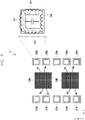
- FIG. 7 is a conceptual diagram illustrating the flow of a current in the antenna module 11 of the electronic device 10, according to various embodiments.
- the plurality of floating radiators 220a to 220d may be electromagnetically coupled to the 1a-th antenna element 110a.
- an electromagnetic field may be induced in each of the plurality of floating radiators 220a to 220d by a first electromagnetic wave radiated from the 1a-th antenna element 110a.
- Each of the plurality of floating radiators 220a to 220d in which the electromagnetic field is induced by the first electromagnetic wave may radiate a second electromagnetic wave by the electromagnetic field.
- the 1a-th floating radiator 220a may radiate a second electromagnetic wave by an electromagnetic field induced from the 1a-th antenna element 110a.
- a 1b-th floating radiator 220b may radiate a second electromagnetic wave by the electromagnetic field induced from the 1a-th antenna element 110a.
- a 1c-th floating radiator 220c may radiate a second electromagnetic wave by the electromagnetic field induced from the 1a-th antenna element 110a.
- a 1d-th floating radiator 220d may radiate a second electromagnetic wave by the electromagnetic field induced from the 1a-th antenna element 110a.
- FIG. 8 is a conceptual diagram illustrating the flow of a current in at least one floating radiator among the plurality of floating radiators 210a to 250c of the antenna module 11 of the electronic device 10, according to various embodiments.
- At least one floating radiator among the plurality of floating radiators 210a to 250c may be designed in a wavelength loop manner.
- the 2a-th floating radiator 220a may be designed in the wavelength loop manner.
- the 2a-th floating radiator 220a designed in the wavelength loop manner may operate as a radiator.
- a horizontal or vertical length d of the 2a-th floating radiator 220a may be determined based on a length ⁇ of wavelength of a first electromagnetic wave radiated from the 1a-th antenna element 110a.
- the horizontal or vertical length d of the 2a-th floating radiator 220a may be 1/4 of the length ⁇ of the wavelength of the first electromagnetic wave radiated from the 1a-th antenna element 110a.
- a total length d ⁇ 4 of the 2a-th floating radiator 220a may be the same as the length ⁇ of the wavelength of the first electromagnetic wave radiated from the 1a-th antenna element 110a.
- the polarization of the first electromagnetic wave radiated from the 1a-th antenna element 110a may be in a z-axis direction or close to the z-axis direction with reference to the upper surface of the 1a-th antenna element 110a.
- a horizontal component of a current in an electromagnetic field induced in the 2a-th floating radiator 220a having a horizontal or vertical length of ⁇ /4 may be extinguished by mutual interference between upper and lower surfaces of the 2a-th floating radiator 220a. Therefore, in the electromagnetic field induced in the 2a-th floating radiator 220a, the horizontal component of the current may be extinguished and only a vertical component may exist.
- a direction of a current of the 1a-th antenna element 110a may be the same as or similar to a direction of a current flowing through the 2a-th floating radiator 220a.
- the antenna module 11 may have a wider aperture due to the plurality of floating radiators 210a to 250c and the plurality of antenna elements 110a to 140c having the same or similar current direction.
- a shape and size of each of the plurality of floating radiators 210a to 250j may be the same as or similar to a shape and size of at least one of the floating radiators of FIGS. 9 to 13 .
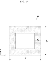
- FIG. 9 is a conceptual diagram illustrating at least one floating radiator among the plurality of floating radiators 210a to 250c of the antenna module 11 of the electronic device 10, according to various embodiments.
- a floating radiator 900 may have a rectangular ring shape.
- the floating radiator 400 may be the same as or similar to at least one of the plurality of floating radiators 210a to 250j of FIG. 3 .
- a horizontal length w9, a vertical length d9, and a line width w'9 of the floating radiator 900 may be determined based on the magnitude of wavelength of an electromagnetic field output from the plurality of antenna elements 110a to 140c of FIG. 3 .
- a factor value of each of the plurality of inductors 511 to 514 and the capacitor 520 of FIG. 5 may be determined according to at least one of the horizontal length w9, the vertical length d9, and the line width w'9 of the floating radiator 900.
- an imaginary component of the factor value of each of the plurality of inductors 511 to 514 and the capacitor 520 may be determined according to at least one of the horizontal length w9, the vertical length d9, and the line width w'9 of the floating radiator 900.
- an imaginary component of an inductance value of each of the plurality of inductors 511 to 514 and an imaginary component of a capacitance value of the capacitor 520 may be determined according to at least one of the horizontal length w9, the vertical length d9, and the line width w'9 of the floating radiator 900.
- a direction of a second electromagnetic wave radiated from the floating radiator 900 may be determined based on the imaginary component of the factor value of each of the plurality of inductors 511 to 514 and the capacitor 520 of FIG. 5 .
- the direction of the second electromagnetic wave radiated from the floating radiator 900 may be determined based on at least one of the horizontal length w9, the vertical length d9, and the line width w'9 of the floating radiator 900.
- At least one of the horizontal length w9, the vertical length d9, and the line width w'9 of the floating radiator 900 may be determined such that a radiation direction of a second electromagnetic wave radiated from the floating radiator 900 is the same as a radiation direction of a first electromagnetic wave radiated from the 1a-th antenna element 110a.
- FIG. 10 is a conceptual diagram illustrating at least one floating radiator among the plurality of floating radiators 210a to 250c of the antenna module 11 of the electronic device 10, according to various embodiments.
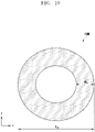
- a floating radiator 1000 may have a circular ring shape.
- the floating radiator 1000 may be the same as or similar to at least one of the plurality of floating radiators 210a to 250j of FIG. 3 .
- a line width w10 and a length d10 of a diameter of the floating radiator 1000 may be determined based on the magnitude of wavelength of an electromagnetic field output from the plurality of antenna elements 110a to 140c of FIG. 3 .
- a factor value of each of the plurality of inductors 511 to 514 and the capacitor 520 of FIG. 5 may be determined according to at least one of the line width w10 and the length d10 of the diameter of the floating radiator 1000.
- an imaginary component of the factor value of each of the plurality of inductors 511 to 514 and the capacitor 520 may be determined according to at least one of the line width w10 and the length d10 of the diameter of the floating radiator 1000.
- an imaginary component of an inductance value of each of the plurality of inductors 511 to 514 and an imaginary component of a capacitance value of the capacitor 520 may be determined according to at least one of the line width w10 and the length d10 of the diameter of the floating radiator 1000.
- a direction of a second electromagnetic wave radiated from the floating radiator 1000 may be determined based on the imaginary component of the factor value of each of the plurality of inductors 511 to 514 and the capacitor 520 of FIG. 5 .
- the direction of the second electromagnetic wave radiated from the floating radiator 1000 may be determined based on at least one of the line width w10 and the length d10 of the diameter of the floating radiator 1000.
- At least one of the line width w10 and the length d10 of the diameter of the floating radiator 1000 may be determined such that a radiation direction of a second electromagnetic wave radiated from the floating radiator 1000 is the same as a radiation direction of a first electromagnetic wave radiated from the 1a-th antenna element 110a.
- FIG. 11 is a conceptual diagram illustrating at least one floating radiator among the plurality of floating radiators 210a to 250c of the antenna module 11 of the electronic device 10, according to various embodiments.
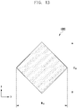
- a floating radiator 1100 may have a diamond-shaped ring shape.
- the floating radiator 1100 may be the same as or similar to at least one of the plurality of floating radiators 210a to 250j of FIG. 3 .
- a horizontal length w11, a vertical length d11, and a line width w'11 of the floating radiator 1100 may be determined based on the magnitude of wavelength of an electromagnetic field output from the plurality of antenna elements 110a to 140c of FIG. 3 .
- a factor value of each of the plurality of inductors 511 to 514 and the capacitor 520 of FIG. 5 may be determined according to at least one of the horizontal length w11, the vertical length d11, and the line width w'11 of the floating radiator 1100.
- an imaginary component of the factor value of each of the plurality of inductors 511 to 514 and the capacitor 520 may be determined according to at least one of the horizontal length w11, the vertical length d11, and the line width w'11 of the floating radiator 1100.
- an imaginary component of an inductance value of each of the plurality of inductors 511 to 514 and an imaginary component of a capacitance value of the capacitor 520 may be determined according to at least one of the horizontal length w11, the vertical length d11, and the line width w'11 of the floating radiator 1100.
- a direction of a second electromagnetic wave radiated from the floating radiator 1100 may be determined based on the imaginary component of the factor value of each of the plurality of inductors 511 to 514 and the capacitor 520 of FIG. 5 .
- the direction of the second electromagnetic wave radiated from the floating radiator 1100 may be determined based on at least one of the horizontal length w11, the vertical length d11, and the line width w'11 of the floating radiator 1100.
- At least one of the horizontal length w11, the vertical length d11, and the line width w'11 of the floating radiator 1100 may be determined such that a radiation direction of a second electromagnetic wave radiated from the floating radiator 1100 is the same as a radiation direction of a first electromagnetic wave radiated from the 1a-th antenna element 110a.
- FIG. 12 is a conceptual diagram illustrating at least one floating radiator among the plurality of floating radiators 210a to 250c of the antenna module 11 of the electronic device 10, according to various embodiments.
- a floating radiator 1200 may be a rectangular patch-type radiator.
- the floating radiator 1200 may be the same as or similar to at least one of the plurality of floating radiators 210a to 250j of FIG. 3 .
- a horizontal length w12 and a vertical length d12 of the floating radiator 1200 may be determined based on the magnitude of wavelength of an electromagnetic field output from the plurality of antenna elements 110a to 140c of FIG. 3 .
- a factor value of each of the plurality of inductors 511 to 514 and the capacitor 520 of FIG. 5 may be determined according to at least one of the horizontal length w12 and the vertical length d12 of the floating radiator 1200.
- an imaginary component of the factor value of each of the plurality of inductors 511 to 514 and the capacitor 520 may be determined according to at least one of the horizontal length w12 and the vertical length d12 of the floating radiator 1200.
- an imaginary component of an inductance value of each of the plurality of inductors 511 to 514 and an imaginary component of a capacitance value of the capacitor 520 may be determined according to at least one of the horizontal length w12 and the vertical length d12 of the floating radiator 1200.
- a direction of a second electromagnetic wave radiated from the floating radiator 1200 may be determined based on the imaginary component of the factor value of each of the plurality of inductors 511 to 514 and the capacitor 520 of FIG. 5 .
- the direction of the second electromagnetic wave radiated from the floating radiator 1200 may be determined based on at least one of the horizontal length w12 and the vertical length d12 of the floating radiator 1200.
- At least one of the horizontal length w12 and the vertical length d12 of the floating radiator 1200 may be determined such that a radiation direction of a second electromagnetic wave radiated from the floating radiator 1200 is the same as a radiation direction of a first electromagnetic wave radiated from the 1a-th antenna element 110a.
- FIG. 13 is a conceptual diagram illustrating at least one floating radiator among the plurality of floating radiators 210a to 250c of the antenna module 11 of the electronic device 10, according to various embodiments.
- a floating radiator 1300 may be a patch-type radiator having a diamond shape.
- the floating radiator 1300 may be the same as or similar to at least one of the plurality of floating radiators 210a to 250j of FIG. 3 .
- a horizontal length w13 and a vertical length d13 of the floating radiator 1300 may be determined based on the magnitude of wavelength of an electromagnetic field output from the plurality of antenna elements 110a to 140c of FIG. 3 .
- a factor value of each of the plurality of inductors 511 to 514 and the capacitor 520 of FIG. 5 may be determined according to at least one of the horizontal length w13 and the vertical length d13 of the floating radiator 1300.
- an imaginary component of the factor value of each of the plurality of inductors 511 to 514 and the capacitor 520 may be determined according to at least one of the horizontal length w13 and the vertical length d13 of the floating radiator 1300.
- an imaginary component of an inductance value of each of the plurality of inductors 511 to 514 and an imaginary component of a capacitance value of the capacitor 520 may be determined according to at least one of the horizontal length w13 and the vertical length d13 of the floating radiator 1300.
- a phase of a second electromagnetic wave radiated from the floating radiator 1300 may be determined based on the imaginary component of the factor value of each of the plurality of inductors 511 to 514 and the capacitor 520 of FIG. 5 .
- the phase of the second electromagnetic wave radiated from the floating radiator 1300 may be determined based on at least one of the horizontal length w13 and the vertical length d13 of the floating radiator 1300. At least one of the horizontal length w13 and the vertical length d13 of the floating radiator 1300 may be determined such that a phase of a second electromagnetic wave radiated from the floating radiator 1300 is the same as a phase of a first electromagnetic wave radiated from the 1a-th antenna element 110a.
- FIG. 14 is a conceptual diagram illustrating radiation characteristics of the antenna module 11 which does not include the plurality of floating radiators 210a to 250c in the electronic device 10, according to various embodiments.
- FIG. 15 is a conceptual diagram illustrating radiation characteristics of the antenna module 11 which includes the plurality of floating radiators 210a to 250c in the electronic device, according to various embodiments.
- a range of an electric field distributed on the surface of the antenna module 11 may be widened.
- the antenna module 11 may have a wide range of electric field distribution due to the plurality of floating radiators 210a to 250c. Accordingly, the width of a beam radiated from the antenna module 11 may be narrowed.
- the antenna module 11 which includes the plurality of floating radiators 210a to 250c may have radiation characteristics as shown in Table 2 below.
- a side ratio of the antenna module 11 of the electronic device 10 which includes the plurality of floating radiators 210a to 250c may have more improved characteristics than a side ratio of the antenna module 11 of the electronic device 10 which does not include the plurality of floating radiators 210a to 250c.
- a rear ratio of the antenna module 11 of the electronic device 10 which includes the plurality of floating radiators 210a to 250c may have more improved characteristics than a rear ratio of the antenna module 11 of the electronic device 10 which does not include the plurality of floating radiators 210a to 250c.
- the disclosure may be used in the electronics industry and the information and communications industry.
Landscapes
- Engineering & Computer Science (AREA)
- Computer Networks & Wireless Communication (AREA)
- Physics & Mathematics (AREA)
- Optics & Photonics (AREA)
- Variable-Direction Aerials And Aerial Arrays (AREA)
Applications Claiming Priority (2)
| Application Number | Priority Date | Filing Date | Title |
|---|---|---|---|
| US202062961754P | 2020-01-16 | 2020-01-16 | |
| PCT/KR2021/000599 WO2021145723A1 (ko) | 2020-01-16 | 2021-01-15 | 통신 시스템에서 플로팅 라디에이터를 포함하는 안테나 모듈 및 이를 포함하는 전자 장치 |
Publications (2)
| Publication Number | Publication Date |
|---|---|
| EP4075596A1 true EP4075596A1 (de) | 2022-10-19 |
| EP4075596A4 EP4075596A4 (de) | 2023-02-22 |
Family
ID=76864556
Family Applications (1)
| Application Number | Title | Priority Date | Filing Date |
|---|---|---|---|
| EP21741861.5A Pending EP4075596A4 (de) | 2020-01-16 | 2021-01-15 | Antennenmodul, das schwimmende strahler in einem kommunikationssystem umfasst, und elektronische vorrichtung, die dasselbe umfasst |
Country Status (5)
| Country | Link |
|---|---|
| US (2) | US12401114B2 (de) |
| EP (1) | EP4075596A4 (de) |
| KR (2) | KR102902612B1 (de) |
| CN (2) | CN120879237A (de) |
| WO (1) | WO2021145723A1 (de) |
Families Citing this family (1)
| Publication number | Priority date | Publication date | Assignee | Title |
|---|---|---|---|---|
| US12489199B2 (en) * | 2022-12-21 | 2025-12-02 | Outdoor Wireless Networks LLC | Base station antennas having partially reflective surface isolation walls |
Family Cites Families (68)
| Publication number | Priority date | Publication date | Assignee | Title |
|---|---|---|---|---|
| US4554549A (en) * | 1983-09-19 | 1985-11-19 | Raytheon Company | Microstrip antenna with circular ring |
| GB8803451D0 (en) * | 1988-02-15 | 1988-03-16 | British Telecomm | Antenna |
| GB9002636D0 (en) * | 1990-02-06 | 1990-04-04 | British Telecomm | Antenna |
| FR2691015B1 (fr) * | 1992-05-05 | 1994-10-07 | Aerospatiale | Antenne-réseau de type micro-ruban à faible épaisseur mais à large bande passante. |
| JPH06326510A (ja) * | 1992-11-18 | 1994-11-25 | Toshiba Corp | ビーム走査アンテナ及びアレーアンテナ |
| US5745079A (en) * | 1996-06-28 | 1998-04-28 | Raytheon Company | Wide-band/dual-band stacked-disc radiators on stacked-dielectric posts phased array antenna |
| SE9700401D0 (sv) * | 1997-02-05 | 1997-02-05 | Allgon Ab | Antenna operating with isolated channels |
| US5949387A (en) * | 1997-04-29 | 1999-09-07 | Trw Inc. | Frequency selective surface (FSS) filter for an antenna |
| SE511911C2 (sv) * | 1997-10-01 | 1999-12-13 | Ericsson Telefon Ab L M | Antennenhet med en flerskiktstruktur |
| US6518931B1 (en) * | 2000-03-15 | 2003-02-11 | Hrl Laboratories, Llc | Vivaldi cloverleaf antenna |
| US7358922B2 (en) * | 2002-12-13 | 2008-04-15 | Commscope, Inc. Of North Carolina | Directed dipole antenna |
| US7385555B2 (en) * | 2004-11-12 | 2008-06-10 | The Mitre Corporation | System for co-planar dual-band micro-strip patch antenna |
| US7289064B2 (en) * | 2005-08-23 | 2007-10-30 | Intel Corporation | Compact multi-band, multi-port antenna |
| US7423608B2 (en) * | 2005-12-20 | 2008-09-09 | Motorola, Inc. | High impedance electromagnetic surface and method |
| EP1942556A1 (de) | 2006-12-29 | 2008-07-09 | LG Electronics Inc. | Antenne und elektronische Geräte mit dieser Antenne |
| KR20080062894A (ko) * | 2006-12-29 | 2008-07-03 | 엘지전자 주식회사 | 안테나 및 이를 구비한 전자기기 |
| US8354972B2 (en) * | 2007-06-06 | 2013-01-15 | Fractus, S.A. | Dual-polarized radiating element, dual-band dual-polarized antenna assembly and dual-polarized antenna array |
| EP2117078B1 (de) * | 2008-05-05 | 2017-07-05 | Nokia Solutions and Networks Oy | Anordnung aus Patchantennenelementen |
| CN101702469A (zh) * | 2009-11-20 | 2010-05-05 | 北京航空航天大学 | X、Ku波段透射Ka波段反射四频点频率选择表面设计方法 |
| CN102754276B (zh) * | 2009-12-07 | 2016-03-02 | 日本电气株式会社 | 表现出超颖材料特性的结构和天线 |
| JP4916036B2 (ja) * | 2010-02-23 | 2012-04-11 | カシオ計算機株式会社 | 複数周波アンテナ |
| US8466844B2 (en) * | 2010-06-16 | 2013-06-18 | Sony Ericsson Mobile Communications Ab | Multi-band antennas using multiple parasitic coupling elements and wireless devices using the same |
| JP5252513B2 (ja) * | 2010-08-31 | 2013-07-31 | カシオ計算機株式会社 | 複数周波円偏波アンテナ |
| CN102176537A (zh) * | 2011-01-17 | 2011-09-07 | 西安电子科技大学 | 用于缩减雷达散射截面的天线 |
| FR2985099B1 (fr) | 2011-12-23 | 2014-01-17 | Alcatel Lucent | Antenne panneau multibande a polarisation croisee |
| FR2994342B1 (fr) * | 2012-07-31 | 2016-02-05 | Eads Europ Aeronautic Defence | Dispositif de decouplage entre antennes - notamment des antennes patchs montees sur un aeronef |
| EP2919323A4 (de) | 2012-11-07 | 2016-07-06 | Murata Manufacturing Co | Gruppenantenne |
| DE102013012305A1 (de) * | 2013-07-24 | 2015-01-29 | Kathrein-Werke Kg | Breitband-Antennenarray |
| CN104347939B (zh) * | 2013-08-05 | 2018-10-26 | 中兴通讯股份有限公司 | 多输入多输出天线系统和辐射吸收方法 |
| DE202015009937U1 (de) * | 2014-04-11 | 2021-10-28 | Commscope Technologies Llc | Mehrbandstrahler-Arrays mit eliminierten Resonanzen |
| WO2016067906A1 (ja) * | 2014-10-30 | 2016-05-06 | 三菱電機株式会社 | アレイアンテナ装置およびその製造方法 |
| US10148012B2 (en) | 2015-02-13 | 2018-12-04 | Commscope Technologies Llc | Base station antenna with dummy elements between subarrays |
| FR3036541B1 (fr) * | 2015-05-19 | 2018-06-29 | Smart Packaging Solutions | Antenne a circuits rlc entremeles |
| JP6512402B2 (ja) * | 2015-05-20 | 2019-05-15 | パナソニックIpマネジメント株式会社 | アンテナ装置、無線通信装置、及びレーダ装置 |
| US20170033461A1 (en) * | 2015-07-27 | 2017-02-02 | Qualcomm Incorporated | Low-profile antenna with high isolation for bluetooth and wifi coexistence |
| EP3168927B1 (de) * | 2015-11-16 | 2022-02-23 | Huawei Technologies Co., Ltd. | Hochkompakte, ultrabreitbandige duale polarisierte basisstationsantenne |
| JP6437942B2 (ja) * | 2016-02-23 | 2018-12-12 | 株式会社Soken | アンテナ装置 |
| JP6742397B2 (ja) * | 2016-03-04 | 2020-08-19 | 株式会社村田製作所 | アレーアンテナ |
| ES2719213T3 (es) * | 2016-03-14 | 2019-07-09 | Kathrein Se | Disposición de radiadores en forma de dipolo |
| CN109643846B (zh) * | 2016-08-24 | 2021-02-23 | 株式会社村田制作所 | 天线模块 |
| US10573974B2 (en) * | 2017-07-07 | 2020-02-25 | Rohde & Schwarz Gmbh & Co. Kg | Antenna array, calibration system as well as method for calibrating an antenna array |
| KR102352592B1 (ko) * | 2017-07-13 | 2022-01-19 | 삼성전자주식회사 | 어레이 안테나를 포함하는 전자 장치 |
| JP2019080298A (ja) | 2017-10-23 | 2019-05-23 | 株式会社村田製作所 | マルチアンテナモジュール及び携帯端末 |
| KR102372187B1 (ko) | 2017-11-24 | 2022-03-08 | 삼성전자주식회사 | 센싱 전극을 포함하는 통신 장치를 포함하는 전자 장치 |
| KR102513750B1 (ko) * | 2017-11-28 | 2023-03-24 | 삼성전자 주식회사 | 도전성 패턴을 포함하는 인쇄회로기판 및 그 인쇄회로기판을 포함하는 전자 장치 |
| KR102428929B1 (ko) * | 2018-01-29 | 2022-08-05 | 삼성전자주식회사 | 기생 도전성 판을 포함하는 안테나 구조 |
| US10886618B2 (en) * | 2018-03-30 | 2021-01-05 | Samsung Electro-Mechanics Co., Ltd. | Antenna apparatus and antenna module |
| US11101562B2 (en) * | 2018-06-13 | 2021-08-24 | Mediatek Inc. | Multi-band dual-polarized antenna structure and wireless communication device using the same |
| WO2020027058A1 (ja) * | 2018-08-02 | 2020-02-06 | 株式会社村田製作所 | アンテナ装置 |
| US10938121B2 (en) * | 2018-09-04 | 2021-03-02 | Mediatek Inc. | Antenna module of improved performances |
| US11296415B2 (en) * | 2018-09-28 | 2022-04-05 | Qualcomm Incorporated | Multi-layer patch antenna |
| TWI682585B (zh) * | 2018-10-04 | 2020-01-11 | 和碩聯合科技股份有限公司 | 天線裝置 |
| US20200303820A1 (en) * | 2019-03-19 | 2020-09-24 | Wilson Electronics, Llc | Antenna with parasitic elements |
| WO2020190863A1 (en) * | 2019-03-21 | 2020-09-24 | Commscope Technologies Llc | Base station antennas having parasitic assemblies for improving cross-polarization discrimination performance |
| KR102639417B1 (ko) * | 2019-05-10 | 2024-02-23 | 삼성전자주식회사 | 안테나를 포함하는 전자 장치 |
| US10804609B1 (en) * | 2019-07-24 | 2020-10-13 | Facebook, Inc. | Circular polarization antenna array |
| KR102607538B1 (ko) * | 2019-08-08 | 2023-11-28 | 삼성전기주식회사 | 안테나 장치 |
| CN112582781A (zh) * | 2019-09-27 | 2021-03-30 | 康普技术有限责任公司 | 辐射元件以及基站天线 |
| KR102650820B1 (ko) * | 2019-11-18 | 2024-03-26 | 삼성전자주식회사 | 안테나 및 그것을 포함하는 전자 장치 |
| KR102254878B1 (ko) * | 2019-11-20 | 2021-05-24 | 삼성전기주식회사 | 칩 안테나 모듈 집합체 |
| US11581648B2 (en) * | 2020-06-08 | 2023-02-14 | The Hong Kong University Of Science And Technology | Multi-port endfire beam-steerable planar antenna |
| CN113782949A (zh) * | 2020-06-10 | 2021-12-10 | 康普技术有限责任公司 | 具有频率选择表面的基站天线 |
| US11581664B2 (en) * | 2020-08-07 | 2023-02-14 | Qualcomm Incorporated | Multiband antennas |
| KR102456278B1 (ko) * | 2020-12-15 | 2022-10-20 | 주식회사 에이스테크놀로지 | 개선된 격리도 특성을 가지는 다중 대역 기지국 안테나 |
| US12003038B2 (en) * | 2021-02-08 | 2024-06-04 | Nokia Technologies Oy | Array of patch antennas |
| CN115173070A (zh) * | 2021-04-02 | 2022-10-11 | 康普技术有限责任公司 | 辐射元件和多频带基站天线 |
| CN115911820A (zh) * | 2021-09-22 | 2023-04-04 | 安弗施无线射频系统(上海)有限公司 | 天线和基站 |
| CN116073120A (zh) * | 2023-03-06 | 2023-05-05 | 安徽大学 | 一种宽带毫米波圆极化天线单元、单模阵列及双模阵列 |
-
2021
- 2021-01-15 EP EP21741861.5A patent/EP4075596A4/de active Pending
- 2021-01-15 CN CN202511003706.8A patent/CN120879237A/zh active Pending
- 2021-01-15 CN CN202180009612.5A patent/CN114982063B/zh active Active
- 2021-01-15 KR KR1020210005920A patent/KR102902612B1/ko active Active
- 2021-01-15 WO PCT/KR2021/000599 patent/WO2021145723A1/ko not_active Ceased
-
2022
- 2022-07-13 US US17/863,857 patent/US12401114B2/en active Active
-
2025
- 2025-08-22 US US19/307,833 patent/US20250392036A1/en active Pending
- 2025-12-16 KR KR1020250201112A patent/KR20260002489A/ko active Pending
Also Published As
| Publication number | Publication date |
|---|---|
| CN114982063B (zh) | 2025-08-08 |
| KR102902612B1 (ko) | 2025-12-19 |
| WO2021145723A1 (ko) | 2021-07-22 |
| EP4075596A4 (de) | 2023-02-22 |
| US20220352648A1 (en) | 2022-11-03 |
| KR20210092696A (ko) | 2021-07-26 |
| CN120879237A (zh) | 2025-10-31 |
| CN114982063A (zh) | 2022-08-30 |
| US20250392036A1 (en) | 2025-12-25 |
| KR20260002489A (ko) | 2026-01-06 |
| US12401114B2 (en) | 2025-08-26 |
Similar Documents
| Publication | Publication Date | Title |
|---|---|---|
| EP3756236B1 (de) | Antennenmodul mit mehreren strahlern und basisstation mit dem antennenmodul | |
| EP3694050A1 (de) | Modul mit antenne und hf-element und basisstation damit | |
| US11063364B2 (en) | Antenna module including dielectric material and electronic device including antenna module | |
| EP3703186B1 (de) | Antennenmodul mit isolator und basisstation mit diesem antennenmodul | |
| US20250392036A1 (en) | Antenna module comprising floating radiators in communication system, and electronic device comprising same | |
| US11233323B2 (en) | Antenna module including metal structure for reducing radio waves radiated toward back lobe and electronic device including the same | |
| CN111799550B (zh) | 包括补偿电气路径差的补偿器的天线模块和包含该天线模块的电子设备 | |
| EP4123832A1 (de) | Antennenvorrichtung mit radom und basisstation damit | |
| KR102904490B1 (ko) | 안테나 모듈 및 이를 포함하는 전자 장치 | |
| EP3490068B1 (de) | Antennenvorrichtung | |
| CA3097520C (en) | Antenna module including dielectric material and electronic device including antenna module | |
| KR20220163033A (ko) | 서브 안테나를 포함하는 안테나 모듈 및 이를 포함하는 전자 장치 |
Legal Events
| Date | Code | Title | Description |
|---|---|---|---|
| STAA | Information on the status of an ep patent application or granted ep patent |
Free format text: STATUS: THE INTERNATIONAL PUBLICATION HAS BEEN MADE |
|
| PUAI | Public reference made under article 153(3) epc to a published international application that has entered the european phase |
Free format text: ORIGINAL CODE: 0009012 |
|
| STAA | Information on the status of an ep patent application or granted ep patent |
Free format text: STATUS: REQUEST FOR EXAMINATION WAS MADE |
|
| 17P | Request for examination filed |
Effective date: 20220714 |
|
| AK | Designated contracting states |
Kind code of ref document: A1 Designated state(s): AL AT BE BG CH CY CZ DE DK EE ES FI FR GB GR HR HU IE IS IT LI LT LU LV MC MK MT NL NO PL PT RO RS SE SI SK SM TR |
|
| REG | Reference to a national code |
Ref country code: DE Ref legal event code: R079 Free format text: PREVIOUS MAIN CLASS: H01Q0001380000 Ipc: H01Q0001240000 |
|
| A4 | Supplementary search report drawn up and despatched |
Effective date: 20230120 |
|
| RIC1 | Information provided on ipc code assigned before grant |
Ipc: H01Q 1/52 20060101ALI20230116BHEP Ipc: H01Q 15/00 20060101ALI20230116BHEP Ipc: H01Q 5/385 20150101ALI20230116BHEP Ipc: H01Q 21/06 20060101ALI20230116BHEP Ipc: H01Q 1/24 20060101AFI20230116BHEP |
|
| DAV | Request for validation of the european patent (deleted) | ||
| DAX | Request for extension of the european patent (deleted) | ||
| STAA | Information on the status of an ep patent application or granted ep patent |
Free format text: STATUS: EXAMINATION IS IN PROGRESS |
|
| 17Q | First examination report despatched |
Effective date: 20240910 |