EP4078202B1 - Procédé et dispositif de détection de champ électrique - Google Patents
Procédé et dispositif de détection de champ électrique Download PDFInfo
- Publication number
- EP4078202B1 EP4078202B1 EP20829305.0A EP20829305A EP4078202B1 EP 4078202 B1 EP4078202 B1 EP 4078202B1 EP 20829305 A EP20829305 A EP 20829305A EP 4078202 B1 EP4078202 B1 EP 4078202B1
- Authority
- EP
- European Patent Office
- Prior art keywords
- sensor
- sensor element
- coupling
- electric field
- counter
- Prior art date
- Legal status (The legal status is an assumption and is not a legal conclusion. Google has not performed a legal analysis and makes no representation as to the accuracy of the status listed.)
- Active
Links
Images


Classifications
-
- G—PHYSICS
- G01—MEASURING; TESTING
- G01R—MEASURING ELECTRIC VARIABLES; MEASURING MAGNETIC VARIABLES
- G01R29/00—Arrangements for measuring or indicating electric quantities not covered by groups G01R19/00 - G01R27/00
- G01R29/12—Measuring electrostatic fields or voltage-potential
-
- G—PHYSICS
- G02—OPTICS
- G02B—OPTICAL ELEMENTS, SYSTEMS OR APPARATUS
- G02B26/00—Optical devices or arrangements for the control of light using movable or deformable optical elements
- G02B26/08—Optical devices or arrangements for the control of light using movable or deformable optical elements for controlling the direction of light
- G02B26/0816—Optical devices or arrangements for the control of light using movable or deformable optical elements for controlling the direction of light by means of one or more reflecting elements
- G02B26/0833—Optical devices or arrangements for the control of light using movable or deformable optical elements for controlling the direction of light by means of one or more reflecting elements the reflecting element being a micromechanical device, e.g. a MEMS mirror, DMD
- G02B26/0841—Optical devices or arrangements for the control of light using movable or deformable optical elements for controlling the direction of light by means of one or more reflecting elements the reflecting element being a micromechanical device, e.g. a MEMS mirror, DMD the reflecting element being moved or deformed by electrostatic means
Definitions
- the invention relates to a sensor for measuring an electric field strength of an electric field, which sensor has a base element and a sensor element with at least one electrical conductor, wherein the sensor element can be deflected from a rest position into a measuring position by the effect of the electric field on the electrical conductor, wherein an evaluation unit is provided for detecting the deflection of the sensor element in the measuring position, wherein a counter element with at least one electrically conductive coupling region is provided, wherein the electrically conductive coupling region on the counter element extends adjacent to the coupling section of the electrical conductor on the sensor element in the rest state of the sensor element.
- Electric field strength is one of the fundamental physical quantities whose quantitative measurement is difficult, especially at low frequencies or static fields.
- One reason for this is the field's susceptibility to disturbance during the measurement itself.
- grounded supply lines and metallic components lead to strong distortion of the electric field.
- Static and low-frequency fields can only be measured in well-defined environments, which makes on-site measurement of such fields, such as in high-voltage systems, very difficult.
- warning devices that warn of high voltages in power supply systems, of impending lightning strikes, or of electrostatic charges.
- Such warning devices can be installed stationary in systems with a potential hazard, for example, crane systems, high-voltage power lines, for lightning warnings at airports, or in grain or wood processing plants.
- a mobile application of such warning systems is required. These can be attached to work clothing or a helmet, for example, and can also be used in the future to monitor compliance with exposure limits for electric fields.
- Mobile use requires a compact design and should be free from the need for calibration and should not be influenced by environmental parameters that are difficult to influence, such as temperature.
- Field mills have been used to measure electric fields. These are based on the change in an electrode potential, which is influenced by the electric field. To generate a measurable change, the electrode must be regularly shielded with another electrode connected to ground. This shielding creates a massive field distortion, which requires complex, location-dependent calibration and compensation processes.
- micromechanical structures consisting of two electrically conductive elements.
- a charge is induced into these elements, creating an attraction between the two elements.
- One of the two elements is mounted so that it can move. This displacement is read, and the electric field strength is determined from it.
- this system has the disadvantage that it is disproportionately insensitive at low field strengths, and the directional information of the field is lost.
- alternating fields generate a constant component that simulates the presence of a direct field.
- the WO 2019 120 795 A1 A device for measuring an electric field (E) with a micromechanical structure made of electrically conductive material.
- the micromechanical structure has a frame section and a movable section.
- An electric field E x in direction x causes an electrical polarization of the micromechanical structure and a force F x .
- This force F x leads to a change in the spatial arrangement of the movable section relative to the frame section in direction x. Detection means are provided to determine this change.
- sensors for measuring an electric field are, for example, from the US 2019 137 555 A1 , the CN 103 675 481 B and the CN 108 508 284 A known.
- the object of the present invention is to propose a sensor for measuring the field strength of an electric field that avoids or at least reduces the disadvantages of the prior art.
- the invention particularly aims to achieve greater measurement accuracy and minimize distortion of the field to be measured.
- the sensor element is preferably elastically mounted on the base element, so that a restoring force acts on the sensor element which is essentially proportional to the deflection of the sensor element from the rest position.
- the rest position refers to the position of the sensor element in the absence of the external electric field, i.e. in the unloaded state.
- the torque acting on the sensor element or its connections to the base element is particularly crucial.
- the proximity of the coupling region and coupling section makes it possible to reduce the conductive surfaces without having to accept a significant reduction in capacitance.
- the part of the conductive surface that is the greatest distance from the gap and has the smallest influence on the capacitance is reduced. Reducing the dimensions of the conductive materials in the measuring volume leads to less field distortion and thus to increased measurement accuracy.
- one end of the sensor element is connected to the base element, with the other end of the sensor element projecting freely.
- the sensor element is designed as a cantilevered part. By connecting the sensor element to the base element on only one side, it is possible to design the freestanding end in different shapes. This allows the mechanical properties of the sensor to be adapted to different properties of the electric field to be measured, for example, with regard to a direct electric field or a low-frequency alternating field, or to different operating conditions, for example, for a mobile application.
- the sensor element has a T-, U-, or bar-shaped basic shape, wherein an interdigital structure can be formed on the T-, U-, or bar-shaped basic shape.
- the T-shaped basic structure makes it possible to increase the gap length between the coupling path and thus the capacitance without changing the mechanical properties of the sensor, in particular the resonant frequency.
- the U-shaped embodiment also aims to increase the capacitance by extending the coupling path.
- the bar structure is structurally particularly simple, which facilitates the manufacture of the sensor. To increase the capacitance in these embodiments, it is advantageous if the sensor element and the counter element have an interdigital structure.
- the counter element is movably mounted on the base element. This allows the mechanically independent deflection of the counter element and the sensor element to be used to determine the electric field strength. This advantageously allows for greater measurement accuracy. Furthermore, error detection can be performed.
- the sensor element two electrical conductors, and the counter element has two electrically conductive coupling regions, wherein the coupling regions on the counter element extend adjacent to the coupling sections of the electrical conductors on the sensor element.
- This embodiment creates two capacitances, which can be arranged, for example, on opposite sides of the sensor element. This makes it possible to spatially separate the two coupling sections, each of which has a charge imprinted on it, from one another on the sensor element while still maintaining a large capacitance value. In addition, the areas of the coupling section and coupling region can be reduced, thereby minimizing the distortion of the electric field to be measured.
- the sensor element has two electrical conductors, which are connected to further voltage sources of different signs.
- This embodiment has a capacitive coupling of the two electrical conductors on the sensor element, which results in an increase in the impressed charge.
- This embodiment is preferably associated with the sensor element being connected to the base element on two opposite sides, and the two coupling sections on the sensor element being located on opposite longitudinal sides (relative to the connecting line between the two connections of the sensor element to the base element).
- a vacuum unit for arranging the sensor element and the counter element in a vacuum.
- it is advantageous to apply high voltages to the coupling section of the sensor element and to the coupling area of the counter element.
- Another possibility is to reduce the width of the gap between the sensor element and the counter element.
- these measures increase the risk of breakdown between the adjacent areas with different potentials.
- the embodiment with a vacuum unit minimizes the risk of breakdown in both cases and thus allows measurements with greater accuracy.
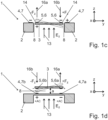
- Figure 1a shows an embodiment of a sensor 1 for measuring an external electric field, in particular a direct electric field.
- the sensor 1 has a base element 2, a sensor element 3, and two counter elements 4 on either side of the sensor element 3.
- Two electrical conductors 5 are applied to the sensor element 3, each forming a coupling section 6.
- the counter elements 4 have electrically conductive coupling regions 7, which are designed for capacitive coupling with the coupling sections 6 of the sensor element 3.
- the coupling region 7 on the counter element 4 and the coupling section 6 on the sensor element 3 run adjacent to one another and are separated from one another by a gap 8.
- the sensor element 3 is connected to the base element 2 via elastic connections 9.
- the sensor element 3 can rotate about a connecting axis 11 between the connection points 12. If the sensor 1 is now located in an electric field 13 to be measured, the forces 16a and 16b act on the charge carriers impressed in the coupling sections 6. Since charges of different signs are impressed in the two coupling sections 6, the force 16a acts on one coupling section 6 in the direction of the electric field 13, and the force 16b acts on the other coupling section 6 in the direction of the electric field 13. Due to the forces 16a and 16b and the distance d ( Fig. 1b ) to the charge carrier concentration center of gravity 14, a moment acts on the sensor element 3.
- the charge carrier concentration center of gravity 14 is located in the outer edge region of the coupling section 6 on the side of the adjacent coupling region 7 of the counter element 4, whereby the distance d (cf. Fig. 1b ) and thus the moment are at a maximum. Due to the capacitive coupling between the coupling region 7 on the counter element 4 and the coupling section 6 on the sensor element 3, a capacitive coupling of the two coupling sections 6 on the sensor element 3 can be dispensed with. Thus, the coupling sections 6 can be formed only at the edges of the sensor element 3, towards the gaps 8, with the central region 15 of the sensor element 3 being free of electrically conductive material. This reduction in the conductive materials in the region of the electric field 13 to be measured reduces distortion of the electric field.
- Figure 1d shows a sensor 1 according to the invention in a further embodiment, wherein the sensor element 3 is arranged at a normal distance a in a plane above the counter element 4.
- the coupling regions 7a and 7b are each connected to the voltage source 10, wherein each of the two coupling regions 7a, 7b is connected to a different output of the voltage source 10a. This creates a potential difference between the two coupling regions 7a and 7b.
- Coupling sections 6a, 6b which are electrically connected to one another, are arranged on the sensor element 3, congruent with the two coupling regions 7a, 7b on the counter element 4. The two coupling sections 6 are capacitively coupled to the two coupling regions 7a, 7b.
- Fig. 1f shows a further embodiment of the sensor 1, in which the sensor element 3 is mounted at a normal distance above the counter element 4.
- the sensor element 3 is located in the same plane as the base element 2 and is connected to it via elastic connections 9.
- the sensor element 3, the base element 2 and the elastic connections 9 are made of conductive material and are electrically connected.
- the counter element 4 is also made of a conductive material and is connected to the base element 2 by an insulator 27, but is electrically insulated from it.
- the gap width of the gap 8 (see Fig. 1g ) is determined by the thickness of the insulator 27.
- the sensor 1 is intended to be positioned in the electric field 13 such that the field lines run parallel to the sensor element 3 and transverse to the elastic connections 9.
- Fig. 1g shows sensor 1 from Figure 1f in a cross-section along line AA.
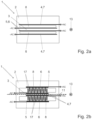
- Fig. 2a shows a further embodiment of the sensor 1, in which the sensor element 3 is designed as a bar.
- Two coupling regions 7 are provided on the counter element 4 and two coupling sections 6 on the sensor element 3.
- the electrical circuitry can be as in the embodiment of the Fig. 1a to 1b be.
- Fig. 2b shows a variant of the sensor of the Fig. 2a , in which the coupling sections 6 on the sensor element 3 and the coupling regions 7 on the counter element 4 form an interdigital structure.
- This interdigital structure increases the capacitance of the sensor between the coupling section 6 and the coupling region 7, and shifts the charge carrier center of gravity further outward (away from the dashed connecting axis), thus increasing the moment acting on the sensor element 3.
- the simple manufacturing and the low susceptibility to external influences are largely retained.
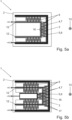
- Fig. 3a shows a sensor 1 with a sensor element 3, which is connected to the base element 2 on two opposite sides, but has only one coupling section 6.
- Two coupling regions 7 are formed on the counter element 4, which are electrically connected to one another.
- the coupling regions 7 are connected to a voltage source 10a.
- the coupling section 6 on the sensor element 3 is connected to another voltage source 10b with a different potential or to another output of the voltage source 10a.
- the capacitive coupling occurs here between the coupling section 6 on the sensor element 3 and the two coupling regions 7 on the counter element 4.
- a force 16 acts on the charge imprinted in the coupling section 6, causing the central region 15 of the sensor element 3 to bulge.
- the advantage of this embodiment lies in its ease of manufacture and robustness against external mechanical influences. Since a transverse movement is the decisive factor here, an external influence in the form of rotation does not significantly affect the measurement result.
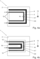
- Fig. 8a shows a further embodiment of the sensor 1, in which a bar-shaped transverse structure 19 is provided at a freely projecting end of the sensor element 3, transverse to the rest of the sensor element 3.
- the sensor element 3 thus has a T-shape.
- the counter element 4 is formed around the sensor element 3 in this embodiment.
- the coupling section 6 is provided on the T-shaped sensor element 3, and the coupling region 7 is provided on the counter element 4.
- the coupling region 7 is connected to the voltage source 10a.
- the coupling section 6 is connected to the further voltage source 10b or to a further output of the voltage source 10a. Due to the additional coupling path along the bar-shaped transverse structure 19 of the sensor element 3, the charge carrier center of gravity 14 is shifted towards the freely projecting end of the sensor element 3, thereby increasing the moment acting on the sensor element 3 and thus the deflection and measurement accuracy.
- Fig. 8b shows a modified embodiment of the sensor 1 of the Fig. 8a , in which an interdigital structure is formed between coupling section 6 and coupling region 7.
- the fingers 17 are provided on the sensor element 3 only on the continuous outer edge of the bar-shaped transverse structure 19, which has the greatest distance from the connection point 12.
- the fingers 17 of the sensor element 3 are opposite the fingers 17 of the counter element 4 in such a way that the fingers 17 interlock and thus form a toothing.
- Fig. 9b shows a sensor 1 with another optical evaluation unit 20, which consists of a transmitter 21 and a receiver 22.
- the transmitter 21 directs a laser beam 24 at a specific angle 23 onto the sensor element 3.
- the laser beam 24 is reflected by the sensor element 3 and picked up by a receiver.
- the receiver delivers a signal that depends on the location at which the reflected laser beam 25 strikes the receiver 22. Deflecting the sensor element 3 changes the reflection angle 26 at which the laser beam 24 is reflected, and thus the location measured by the receiver 22. This allows the strength of the electric field 13 to be measured to be determined.
Landscapes
- Physics & Mathematics (AREA)
- General Physics & Mathematics (AREA)
- Force Measurement Appropriate To Specific Purposes (AREA)
- Measurement Of Length, Angles, Or The Like Using Electric Or Magnetic Means (AREA)
- Measuring Instrument Details And Bridges, And Automatic Balancing Devices (AREA)
Claims (15)
- Capteur (1) pour la mesure de l'intensité d'un champ électrique (13), comprenant :un élément de base (2),un élément de capteur (3) avec au moins un conducteur électrique (5), dans lequel l'élément de capteur (3) peut être dévié, par l'action du champ électrique (13) sur le conducteur électrique (5), d'une position de repos vers une position de mesure (3a),une unité d'analyse (20) pour la mesure de la déviation de l'élément de capteur (3) vers la position de mesure (3a),un contre-élément (4) avec au moins une partie de couplage électro-conductrice (7), dans lequel la partie de couplage électro-conductrice (7) s'étend sur le contre-élément (4), à l'état de repos de l'élément de capteur (3), près d'une portion de couplage (6) du conducteur électrique (5) sur l'élément de capteur (3),caractérisé en ce quela partie de couplage électro-conductrice (7) est reliée, pour le couplage capacitif avec la portion de couplage (6) du conducteur électrique (5) sur l'élément de capteur (3), avec une source de tension (10a), dans lequel la source de tension (10a) est une source de tension à courant alternatif.
- Capteur (1) selon la revendication 1, caractérisé en ce que la partie de couplage (7) sur le contre-élément (4) s'étend parallèlement à la portion de couplage (6) du conducteur électrique (5) sur l'élément de capteur (3).
- Capteur (1) selon la revendication 1 ou 2, caractérisé en ce que la partie de couplage (7) sur le contre-élément (4) et la portion de couplage (6) sur l'élément de capteur (3) forment une structure internumérique.
- Capteur (1) selon l'une des revendications 1 à 3, caractérisé en ce que le contre-élément (4) est disposé, dans la position de repos de l'élément de capteur (3), dans le même plan que l'élément de capteur (3).
- Capteur (1) selon l'une des revendications 1 à 4, caractérisé en ce que le contre-élément (4) est disposé, dans la position de repos de l'élément de capteur (3), parallèlement et à une distance normale par rapport à l'élément de capteur (3).
- Capteur (1) selon l'une des revendications 1 à 5, caractérisé en ce que l'élément de capteur (3) est relié, au niveau de deux extrémités opposées, avec l'élément de base (2).
- Capteur (1) selon l'une des revendications 1 à 6, caractérisé en ce qu'une extrémité de l'élément de capteur (3) est reliée avec l'élément de base (2), dans lequel l'autre extrémité de l'élément de capteur (3) dépasse librement.
- Capteur (1) selon l'une des revendications 1 à 7, caractérisé en ce que l'élément de capteur (3) présente une forme de base en T, en U ou une forme de barre, dans lequel, sur la forme de base en T, en U ou sur la forme de barre, une structure internumérique peut être réalisée.
- Capteur (1) selon l'une des revendications 1 à 8, caractérisé en ce que le contre-élément (4) est constitué d'une seule pièce avec l'élément de base (2).
- Capteur (1) selon l'une des revendications 1 à 9, caractérisé en ce que le contre-élément (4) est logé de manière mobile sur l'élément de base (2).
- Capteur (1) selon l'une des revendications 1 à 10, caractérisé en ce que l'élément de capteur (3) comprend deux conducteurs électriques (5) et le contre-élément (4) comprend deux parties de couplage électro-conductrices (7), dans lequel les parties de couplage électro-conductrices (7) sur le contre-élément (4) s'étendent près des portions de couplage (6) des conducteurs électriques (5) sur l'élément de capteur (3).
- Capteur (1) selon l'une des revendications 1 à 11, caractérisé en ce que le conducteur électrique (5) sur l'élément de capteur (3) est relié avec une autre source de tension (10b), plus particulièrement une source de tension à courant alternatif.
- Capteur (1) selon la revendication 12, caractérisé en ce que l'élément de capteur (3) comprend deux conducteurs électriques (5), qui sont reliés avec d'autres sources de tension (10b) de signes différents.
- Capteur (1) selon l'une des revendications 1 à 11, caractérisé en ce que la source de tension (10a) est conçue pour appliquer, par induction, une charge dans le conducteur électrique (5) de l'élément de capteur (3).
- Procédé de mesure de l'intensité d'un champ électrique (13) avec les étapes suivantes :disposition d'un capteur (1) selon l'une des revendications 1 à 14,déviation de l'élément de capteur (3) par l'action du champ électrique (13) sur le conducteur électrique (5) de la position de repos à la position de mesure etmesure de la déviation de l'élément de capteur (3) dans la position de mesure.
Applications Claiming Priority (2)
| Application Number | Priority Date | Filing Date | Title |
|---|---|---|---|
| ATA51104/2019A AT523342B1 (de) | 2019-12-18 | 2019-12-18 | Sensor |
| PCT/AT2020/060478 WO2021119710A1 (fr) | 2019-12-18 | 2020-12-18 | Procédé et dispositif de détection de champ électrique |
Publications (3)
| Publication Number | Publication Date |
|---|---|
| EP4078202A1 EP4078202A1 (fr) | 2022-10-26 |
| EP4078202B1 true EP4078202B1 (fr) | 2025-04-09 |
| EP4078202C0 EP4078202C0 (fr) | 2025-04-09 |
Family
ID=74045359
Family Applications (1)
| Application Number | Title | Priority Date | Filing Date |
|---|---|---|---|
| EP20829305.0A Active EP4078202B1 (fr) | 2019-12-18 | 2020-12-18 | Procédé et dispositif de détection de champ électrique |
Country Status (3)
| Country | Link |
|---|---|
| EP (1) | EP4078202B1 (fr) |
| AT (1) | AT523342B1 (fr) |
| WO (1) | WO2021119710A1 (fr) |
Family Cites Families (8)
| Publication number | Priority date | Publication date | Assignee | Title |
|---|---|---|---|---|
| AU2002335243A1 (en) * | 2002-10-10 | 2004-05-04 | Fujitsu Media Devices Limited | Micro moving element comprising torsion bar |
| JP2004294351A (ja) * | 2003-03-28 | 2004-10-21 | Canon Inc | 電位センサおよび画像形成装置 |
| CN103675481B (zh) * | 2013-10-18 | 2016-06-15 | 中国科学院电子学研究所 | 压电悬臂梁式微型电场传感器 |
| CN106645999B (zh) * | 2016-09-20 | 2023-01-24 | 西北工业大学 | 一种超高灵敏度的微机械谐振式静电计 |
| CA3022581A1 (fr) * | 2017-11-09 | 2019-05-09 | Janaranjana Sampath Hiniduma Liyanage | Capteur de champ electrique a mouvement de torsion dote de sensibilite modulee et sans reference |
| AT520811B1 (de) * | 2017-12-20 | 2021-06-15 | Donau Univ Krems | Vorrichtung zur messung eines elektrischen felds |
| CN108508284A (zh) * | 2018-03-26 | 2018-09-07 | 中国科学院电子学研究所 | 一种基于扭转振动的互屏蔽式电场传感器 |
| CN109655674B (zh) * | 2019-02-27 | 2021-01-15 | 西北工业大学 | 基于弱耦合微机械谐振器的微弱静电场测量装置及方法 |
-
2019
- 2019-12-18 AT ATA51104/2019A patent/AT523342B1/de active
-
2020
- 2020-12-18 WO PCT/AT2020/060478 patent/WO2021119710A1/fr not_active Ceased
- 2020-12-18 EP EP20829305.0A patent/EP4078202B1/fr active Active
Also Published As
| Publication number | Publication date |
|---|---|
| EP4078202A1 (fr) | 2022-10-26 |
| EP4078202C0 (fr) | 2025-04-09 |
| AT523342A1 (de) | 2021-07-15 |
| WO2021119710A1 (fr) | 2021-06-24 |
| AT523342B1 (de) | 2024-03-15 |
Similar Documents
| Publication | Publication Date | Title |
|---|---|---|
| DE102009046807B4 (de) | Verfahren zur Empfindlichkeitsbestimmung eines Beschleunigungs- oder Magnetfeldsensors | |
| EP2064532B1 (fr) | Système pour déterminer la pression dans un pneumatique de véhicule et/ou la vitesse du véhicule | |
| DE102010012441B4 (de) | Millinewton-Mikrokraftmesser und Verfahren zum Herstellen eines Millinewton-Mikrokraftmessers | |
| DE3625411A1 (de) | Kapazitiver beschleunigungssensor | |
| DE102009026462A1 (de) | Beschleunigungssensor | |
| EP2227674B1 (fr) | Capteur de vitesse de rotation | |
| DE102005003684B4 (de) | Feinjustierungsmechanismus zur Rastersondenmikroskopie | |
| WO1999014613A1 (fr) | Element detecteur | |
| DE102009028343B4 (de) | Sensorelement und Verfahren zum Betrieb eines Sensorelements | |
| EP4078202B1 (fr) | Procédé et dispositif de détection de champ électrique | |
| EP2425208B1 (fr) | Élément de mesure | |
| DE112006003699B4 (de) | Auslenkbares mikromechanisches System sowie dessen Verwendung | |
| DE102010012701B4 (de) | Mikrokraftsensor | |
| DE69611328T2 (de) | Aufprallsensor | |
| WO2000028293A1 (fr) | Capteur de mesure capacitif et son procede d'utilisation | |
| DE19813941A1 (de) | Mikromechanischer Beschleunigungssensor | |
| EP1903326B1 (fr) | Dispositif destiné à la détermination de moments de torsion inférieurs au micro-Newton-mètre | |
| DE102011080982B4 (de) | Sensoranordnung | |
| DE102010039236B4 (de) | Sensoranordnung und Verfahren zum Abgleich einer Sensoranordnung | |
| DE102013107212A1 (de) | Kapazitive Kraftmessvorrichtung | |
| EP2720021B1 (fr) | Dispositif de mesure de force | |
| DE102013224235B4 (de) | Sensorsystem zur kapazitiven Abstandsmessung | |
| DE102007046306B4 (de) | Beschleunigungssensor | |
| DE102008063797A1 (de) | Messgerät | |
| EP3060933B1 (fr) | Magnétomètre à gradients, et procédé de détermination d'un composant individuel d'un capteur à gradients d'un champ magnétique |
Legal Events
| Date | Code | Title | Description |
|---|---|---|---|
| STAA | Information on the status of an ep patent application or granted ep patent |
Free format text: STATUS: UNKNOWN |
|
| STAA | Information on the status of an ep patent application or granted ep patent |
Free format text: STATUS: THE INTERNATIONAL PUBLICATION HAS BEEN MADE |
|
| PUAI | Public reference made under article 153(3) epc to a published international application that has entered the european phase |
Free format text: ORIGINAL CODE: 0009012 |
|
| STAA | Information on the status of an ep patent application or granted ep patent |
Free format text: STATUS: REQUEST FOR EXAMINATION WAS MADE |
|
| 17P | Request for examination filed |
Effective date: 20220718 |
|
| AK | Designated contracting states |
Kind code of ref document: A1 Designated state(s): AL AT BE BG CH CY CZ DE DK EE ES FI FR GB GR HR HU IE IS IT LI LT LU LV MC MK MT NL NO PL PT RO RS SE SI SK SM TR |
|
| DAV | Request for validation of the european patent (deleted) | ||
| DAX | Request for extension of the european patent (deleted) | ||
| GRAP | Despatch of communication of intention to grant a patent |
Free format text: ORIGINAL CODE: EPIDOSNIGR1 |
|
| STAA | Information on the status of an ep patent application or granted ep patent |
Free format text: STATUS: GRANT OF PATENT IS INTENDED |
|
| RIC1 | Information provided on ipc code assigned before grant |
Ipc: G02B 26/08 20060101ALN20241009BHEP Ipc: G01R 29/12 20060101AFI20241009BHEP |
|
| INTG | Intention to grant announced |
Effective date: 20241112 |
|
| GRAS | Grant fee paid |
Free format text: ORIGINAL CODE: EPIDOSNIGR3 |
|
| GRAA | (expected) grant |
Free format text: ORIGINAL CODE: 0009210 |
|
| STAA | Information on the status of an ep patent application or granted ep patent |
Free format text: STATUS: THE PATENT HAS BEEN GRANTED |
|
| AK | Designated contracting states |
Kind code of ref document: B1 Designated state(s): AL AT BE BG CH CY CZ DE DK EE ES FI FR GB GR HR HU IE IS IT LI LT LU LV MC MK MT NL NO PL PT RO RS SE SI SK SM TR |
|
| REG | Reference to a national code |
Ref country code: GB Ref legal event code: FG4D Free format text: NOT ENGLISH |
|
| REG | Reference to a national code |
Ref country code: CH Ref legal event code: EP |
|
| REG | Reference to a national code |
Ref country code: DE Ref legal event code: R096 Ref document number: 502020010811 Country of ref document: DE |
|
| REG | Reference to a national code |
Ref country code: IE Ref legal event code: FG4D Free format text: LANGUAGE OF EP DOCUMENT: GERMAN |
|
| U01 | Request for unitary effect filed |
Effective date: 20250423 |
|
| U07 | Unitary effect registered |
Designated state(s): AT BE BG DE DK EE FI FR IT LT LU LV MT NL PT RO SE SI Effective date: 20250428 |
|
| PG25 | Lapsed in a contracting state [announced via postgrant information from national office to epo] |
Ref country code: ES Free format text: LAPSE BECAUSE OF FAILURE TO SUBMIT A TRANSLATION OF THE DESCRIPTION OR TO PAY THE FEE WITHIN THE PRESCRIBED TIME-LIMIT Effective date: 20250409 |
|
| PG25 | Lapsed in a contracting state [announced via postgrant information from national office to epo] |
Ref country code: GR Free format text: LAPSE BECAUSE OF FAILURE TO SUBMIT A TRANSLATION OF THE DESCRIPTION OR TO PAY THE FEE WITHIN THE PRESCRIBED TIME-LIMIT Effective date: 20250710 Ref country code: NO Free format text: LAPSE BECAUSE OF FAILURE TO SUBMIT A TRANSLATION OF THE DESCRIPTION OR TO PAY THE FEE WITHIN THE PRESCRIBED TIME-LIMIT Effective date: 20250709 |
|
| PG25 | Lapsed in a contracting state [announced via postgrant information from national office to epo] |
Ref country code: PL Free format text: LAPSE BECAUSE OF FAILURE TO SUBMIT A TRANSLATION OF THE DESCRIPTION OR TO PAY THE FEE WITHIN THE PRESCRIBED TIME-LIMIT Effective date: 20250409 |
|
| PG25 | Lapsed in a contracting state [announced via postgrant information from national office to epo] |
Ref country code: HR Free format text: LAPSE BECAUSE OF FAILURE TO SUBMIT A TRANSLATION OF THE DESCRIPTION OR TO PAY THE FEE WITHIN THE PRESCRIBED TIME-LIMIT Effective date: 20250409 |
|
| PG25 | Lapsed in a contracting state [announced via postgrant information from national office to epo] |
Ref country code: RS Free format text: LAPSE BECAUSE OF FAILURE TO SUBMIT A TRANSLATION OF THE DESCRIPTION OR TO PAY THE FEE WITHIN THE PRESCRIBED TIME-LIMIT Effective date: 20250709 |
|
| PG25 | Lapsed in a contracting state [announced via postgrant information from national office to epo] |
Ref country code: IS Free format text: LAPSE BECAUSE OF FAILURE TO SUBMIT A TRANSLATION OF THE DESCRIPTION OR TO PAY THE FEE WITHIN THE PRESCRIBED TIME-LIMIT Effective date: 20250809 |
|
| PG25 | Lapsed in a contracting state [announced via postgrant information from national office to epo] |
Ref country code: SM Free format text: LAPSE BECAUSE OF FAILURE TO SUBMIT A TRANSLATION OF THE DESCRIPTION OR TO PAY THE FEE WITHIN THE PRESCRIBED TIME-LIMIT Effective date: 20250409 |
|
| PG25 | Lapsed in a contracting state [announced via postgrant information from national office to epo] |
Ref country code: CZ Free format text: LAPSE BECAUSE OF FAILURE TO SUBMIT A TRANSLATION OF THE DESCRIPTION OR TO PAY THE FEE WITHIN THE PRESCRIBED TIME-LIMIT Effective date: 20250409 |
|
| PG25 | Lapsed in a contracting state [announced via postgrant information from national office to epo] |
Ref country code: SK Free format text: LAPSE BECAUSE OF FAILURE TO SUBMIT A TRANSLATION OF THE DESCRIPTION OR TO PAY THE FEE WITHIN THE PRESCRIBED TIME-LIMIT Effective date: 20250409 |
|
| PLBE | No opposition filed within time limit |
Free format text: ORIGINAL CODE: 0009261 |
|
| STAA | Information on the status of an ep patent application or granted ep patent |
Free format text: STATUS: NO OPPOSITION FILED WITHIN TIME LIMIT |
|
| REG | Reference to a national code |
Ref country code: CH Ref legal event code: L10 Free format text: ST27 STATUS EVENT CODE: U-0-0-L10-L00 (AS PROVIDED BY THE NATIONAL OFFICE) Effective date: 20260218 |
|
| 26N | No opposition filed |
Effective date: 20260112 |