EP4080227B1 - Circuit de détection de condensateur, capteur, puce et dispositif électronique - Google Patents
Circuit de détection de condensateur, capteur, puce et dispositif électronique Download PDFInfo
- Publication number
- EP4080227B1 EP4080227B1 EP20922556.4A EP20922556A EP4080227B1 EP 4080227 B1 EP4080227 B1 EP 4080227B1 EP 20922556 A EP20922556 A EP 20922556A EP 4080227 B1 EP4080227 B1 EP 4080227B1
- Authority
- EP
- European Patent Office
- Prior art keywords
- switch
- capacitor
- detected
- terminal
- voltage
- Prior art date
- Legal status (The legal status is an assumption and is not a legal conclusion. Google has not performed a legal analysis and makes no representation as to the accuracy of the status listed.)
- Active
Links
Images



Classifications
-
- H—ELECTRICITY
- H03—ELECTRONIC CIRCUITRY
- H03K—PULSE TECHNIQUE
- H03K17/00—Electronic switching or gating, i.e. not by contact-making and –breaking
- H03K17/94—Electronic switching or gating, i.e. not by contact-making and –breaking characterised by the way in which the control signals are generated
- H03K17/96—Touch switches
- H03K17/962—Capacitive touch switches
-
- G—PHYSICS
- G01—MEASURING; TESTING
- G01R—MEASURING ELECTRIC VARIABLES; MEASURING MAGNETIC VARIABLES
- G01R27/00—Arrangements for measuring resistance, reactance, impedance, or electric characteristics derived therefrom
- G01R27/02—Measuring real or complex resistance, reactance, impedance, or other two-pole characteristics derived therefrom, e.g. time constant
- G01R27/26—Measuring inductance or capacitance; Measuring quality factor, e.g. by using the resonance method; Measuring loss factor; Measuring dielectric constants ; Measuring impedance or related variables
- G01R27/2605—Measuring capacitance
-
- G—PHYSICS
- G06—COMPUTING OR CALCULATING; COUNTING
- G06F—ELECTRIC DIGITAL DATA PROCESSING
- G06F3/00—Input arrangements for transferring data to be processed into a form capable of being handled by the computer; Output arrangements for transferring data from processing unit to output unit, e.g. interface arrangements
- G06F3/01—Input arrangements or combined input and output arrangements for interaction between user and computer
- G06F3/03—Arrangements for converting the position or the displacement of a member into a coded form
- G06F3/041—Digitisers, e.g. for touch screens or touch pads, characterised by the transducing means
- G06F3/044—Digitisers, e.g. for touch screens or touch pads, characterised by the transducing means by capacitive means
-
- G—PHYSICS
- G01—MEASURING; TESTING
- G01D—MEASURING NOT SPECIALLY ADAPTED FOR A SPECIFIC VARIABLE; ARRANGEMENTS FOR MEASURING TWO OR MORE VARIABLES NOT COVERED IN A SINGLE OTHER SUBCLASS; TARIFF METERING APPARATUS; MEASURING OR TESTING NOT OTHERWISE PROVIDED FOR
- G01D21/00—Measuring or testing not otherwise provided for
- G01D21/02—Measuring two or more variables by means not covered by a single other subclass
-
- G—PHYSICS
- G01—MEASURING; TESTING
- G01D—MEASURING NOT SPECIALLY ADAPTED FOR A SPECIFIC VARIABLE; ARRANGEMENTS FOR MEASURING TWO OR MORE VARIABLES NOT COVERED IN A SINGLE OTHER SUBCLASS; TARIFF METERING APPARATUS; MEASURING OR TESTING NOT OTHERWISE PROVIDED FOR
- G01D5/00—Mechanical means for transferring the output of a sensing member; Means for converting the output of a sensing member to another variable where the form or nature of the sensing member does not constrain the means for converting; Transducers not specially adapted for a specific variable
- G01D5/12—Mechanical means for transferring the output of a sensing member; Means for converting the output of a sensing member to another variable where the form or nature of the sensing member does not constrain the means for converting; Transducers not specially adapted for a specific variable using electric or magnetic means
- G01D5/14—Mechanical means for transferring the output of a sensing member; Means for converting the output of a sensing member to another variable where the form or nature of the sensing member does not constrain the means for converting; Transducers not specially adapted for a specific variable using electric or magnetic means influencing the magnitude of a current or voltage
- G01D5/24—Mechanical means for transferring the output of a sensing member; Means for converting the output of a sensing member to another variable where the form or nature of the sensing member does not constrain the means for converting; Transducers not specially adapted for a specific variable using electric or magnetic means influencing the magnitude of a current or voltage by varying capacitance
-
- G—PHYSICS
- G01—MEASURING; TESTING
- G01R—MEASURING ELECTRIC VARIABLES; MEASURING MAGNETIC VARIABLES
- G01R19/00—Arrangements for measuring currents or voltages or for indicating presence or sign thereof
- G01R19/0038—Circuits for comparing several input signals and for indicating the result of this comparison, e.g. equal, different, greater, smaller (comparing pulses or pulse trains according to amplitude)
-
- G—PHYSICS
- G01—MEASURING; TESTING
- G01R—MEASURING ELECTRIC VARIABLES; MEASURING MAGNETIC VARIABLES
- G01R19/00—Arrangements for measuring currents or voltages or for indicating presence or sign thereof
- G01R19/165—Indicating that current or voltage is either above or below a predetermined value or within or outside a predetermined range of values
- G01R19/16528—Indicating that current or voltage is either above or below a predetermined value or within or outside a predetermined range of values using digital techniques or performing arithmetic operations
-
- G—PHYSICS
- G01—MEASURING; TESTING
- G01R—MEASURING ELECTRIC VARIABLES; MEASURING MAGNETIC VARIABLES
- G01R19/00—Arrangements for measuring currents or voltages or for indicating presence or sign thereof
- G01R19/165—Indicating that current or voltage is either above or below a predetermined value or within or outside a predetermined range of values
- G01R19/16566—Circuits and arrangements for comparing voltage or current with one or several thresholds and for indicating the result not covered by subgroups G01R19/16504, G01R19/16528, G01R19/16533
-
- G—PHYSICS
- G01—MEASURING; TESTING
- G01R—MEASURING ELECTRIC VARIABLES; MEASURING MAGNETIC VARIABLES
- G01R19/00—Arrangements for measuring currents or voltages or for indicating presence or sign thereof
- G01R19/25—Arrangements for measuring currents or voltages or for indicating presence or sign thereof using digital measurement techniques
- G01R19/257—Arrangements for measuring currents or voltages or for indicating presence or sign thereof using digital measurement techniques using analogue/digital converters of the type with comparison of different reference values with the value of voltage or current, e.g. using step-by-step method
-
- G—PHYSICS
- G01—MEASURING; TESTING
- G01R—MEASURING ELECTRIC VARIABLES; MEASURING MAGNETIC VARIABLES
- G01R23/00—Arrangements for measuring frequencies; Arrangements for analysing frequency spectra
- G01R23/16—Spectrum analysis; Fourier analysis
- G01R23/165—Spectrum analysis; Fourier analysis using filters
-
- H—ELECTRICITY
- H03—ELECTRONIC CIRCUITRY
- H03K—PULSE TECHNIQUE
- H03K2217/00—Indexing scheme related to electronic switching or gating, i.e. not by contact-making or -breaking covered by H03K17/00
- H03K2217/94—Indexing scheme related to electronic switching or gating, i.e. not by contact-making or -breaking covered by H03K17/00 characterised by the way in which the control signal is generated
- H03K2217/96—Touch switches
- H03K2217/9607—Capacitive touch switches
- H03K2217/96071—Capacitive touch switches characterised by the detection principle
- H03K2217/960725—Charge-transfer
Definitions
- US 2014176482A1 discloses an interference tolerant capacitive touch sensor readout circuit, and in particular discloses a circuit layout of a mutual capacitive touch sensor.
- Some embodiments of the present disclosure are intended to provide a capacitance detection circuit, a sensor, a chip and an electronic device, which may digitize a capacitance of a capacitor to be detected without an analog circuit such as an analog-to-digital converter, thereby realizing a simple circuit structure and reducing the power consumption and cost.
- the capacitance of the capacitor to be detected may be digitized without the analog circuit such as the analog-to-digital converter, thereby realizing a simple circuit structure and reducing the power consumption and cost. Furthermore, the anti-interference ability of the capacitance detection circuit may be improved by increasing the charge and discharge times of the capacitor to be detected.
- the measurement of a capacitance of the capacitance sensor is one of the core steps.
- the measurement of the capacitance value is generally realized by an analog circuit including an analog-to-digital converter (ADC), which has high power consumption and cost. Based on this, the inventor proposes the technical solution of the present disclosure.
- ADC analog-to-digital converter
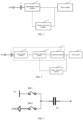
- the capacitance detection circuit includes a capacitance control module 1, a charge conversion module 2 and a filter module 3 which are connected with each other.
- a capacitor C x to be detected is connected to the capacitance control module 1 in series or in parallel.
- the capacitor C x to be detected being connected to the capacitance control module 1 in series is taken as an example, one terminal of the capacitor C x to be detected is connected to the capacitance control module 1, and the other terminal of the capacitor C x to be detected is grounded (GND).
- the capacitance control module 1 is configured to control the capacitor C x to be detected to be charged and discharged for multiple times and generate a digital voltage signal according to an amount of received charges.
- the capacitor C x to be detected releases all stored charges after being charged to a preset voltage during each charge and discharge.
- the capacitance control module controls the capacitor to be detected to be charged and discharged for multiple times.
- the capacitor to be detected releases all stored charges after being charged to the preset voltage during each charge and discharge.
- the capacitance control module may output a corresponding digital voltage signal according to the amount of received charges. In response to the digital voltage signal being at a low level, the capacitance control module only accepts the charges released by the capacitor to be detected.
- the charge conversion module In response to the digital voltage signal being at a high level, the charge conversion module outputs the negative charges with the preset charge amount to the capacitance control module, that is, the capacitance control module receives the charges output by both the capacitor to be detected and the charge conversion module, and then after the capacitor to be detected is charged and discharged for multiple times, the filter module may obtain the value representing the capacitance of the capacitor to be detected according to the digital voltage signal generated after the capacitor to be detected is charged and discharged for multiple times.
- the capacitance of the capacitor to be detected may be digitized without the analog circuit such as the analog-to-digital converter, thereby realizing a simple circuit structure and reducing the power consumption and cost. Furthermore, the anti-interference ability of the capacitance detection circuit may be improved by increasing the charge and discharge times of the capacitor to be detected.
- the capacitance control module 1 includes a charge transfer module 11, a voltage conversion module 12 and a comparison module 13 which are connected in sequence.
- the capacitor C x to be detected is connected to the charge transfer module 11 (which is taken as an example in FIG. 2 ), or the capacitor C x to be detected is connected to both the charge transfer module 11 and the voltage conversion module 12.
- the charge transfer module 11 is configured to control the capacitor C x to be detected to be charged and discharged for multiple times. During each charge and discharge of the capacitor C x to be detected, the capacitor C x to be detected releases all the stored charges to the voltage conversion module 12 after being charged to a preset voltage V tx , that is, a process of each charge and discharge is equivalent to a process of each charge transfer of the capacitor C x to be detected.
- the voltage conversion module 12 is configured to convert the received charges into an analog voltage signal. Specifically, the voltage conversion module 12 may receive the charges of the capacitor C x to be detected during each charge and discharge of the capacitor C x to be detected, and convert the inflowing charges into a voltage to output. The amount of the charges received by the voltage conversion module 12 may change after each charge and discharge of the capacitor C x to be detected, which also makes the voltage output by the voltage conversion module 12 change. Multiple voltages output by the voltage conversion module 12 may form a continuous analog voltage signal after the capacitor C x to be detected is controlled to be charged and discharged for multiple times.
- the comparison module 13 is configured to output the digital voltage signal according to a preset voltage threshold and the analog voltage signal. Specifically, the comparison module 13 compares a current voltage value with the preset voltage threshold after receiving the analog voltage signal sent by the voltage conversion module 12. When the voltage value is greater than the voltage threshold, the output digital signal is at a high level 1. When the voltage value is less than the voltage threshold, the output digital signal is at a low level 0. Therefore, the comparison module 13 outputs a high or low level signal according to the voltage values at different times (different charge and discharge times) after receiving the analog voltage signal, thus forming the digital voltage signal.
- the voltage threshold of the comparison module 13 may be half of the preset voltage V tx .
- the charge conversion module 2 In response to the digital voltage signal being at the high level, the charge conversion module 2 is configured to output the negative charges with the preset charge amount to the voltage conversion module 12.
- the preset charge amount is greater than or equal to the amount of the stored charge when the capacitor C x to be detected is charged to the preset voltage. It should be noted that in this embodiment, the charge conversion module 2 outputting the negative charges is taken as an example, but the invention is not limited to such exemplification.
- the charge conversion module 2 may also be set to output positive charges, as long as an inverse adder is provided in the voltage conversion module 12.
- the filter module 3 is configured to obtain the value representing the capacitance of the capacitor C x to be detected according to the digital voltage signal generated after the capacitor C x to be detected is charged and discharged for multiple times. Specifically, as described above, each charge and discharge of the capacitor C x to be detected corresponds to one value of the digital voltage signal, which may be 0 or 1. Then the number of values 1 in the digital voltage signal corresponding to multiple charges and discharges may be counted, and the number is the value representing the capacitance of the capacitor C x to be detected. The value may be input into a processor of an electronic device after being obtained, so that the processor may obtain the capacitance of the capacitor C x to be detected according to a preset measurement range of the capacitance detection circuit.
- the charge transfer is performed on the capacitor C x to be detected first for multiple times during digitizing the capacitance of the capacitor C x to be detected.
- the voltage conversion module 12 may receive the charges of each discharge of the capacitor C x to be detected which are transferred by the charge transfer module 11 during each charge transfer of the capacitor C x to be detected.
- a voltage value of the analog voltage signal output by the voltage conversion module 12 is less than the voltage threshold, and the digital voltage signal output by the comparison module 13 is at a low level. At this time, the charges received by the voltage conversion module 12 only comes from the capacitor C x to be detected.
- the charge conversion module 2 sends the negative charges with the preset charge amount to the voltage conversion module 12. That is, the voltage conversion module 12 receives both the charges discharged by the capacitor C x to be detected and the negative charges sent by the charge conversion module 2.
- the preset charge amount is greater than or equal to the amount of the stored charges when the capacitor C x to be detected is charged to the preset voltage
- the charges accumulated in the voltage conversion module 12 is consumed, which results in the amount of the charges accumulated in the voltage conversion module 12 less than the critical value Q max
- the voltage value of the analog voltage signal output by the voltage conversion module 12 is less than the voltage threshold
- the digital voltage signal output by the comparison module 13 is at a low level
- the voltage conversion module 12 continues to accumulate charges until the amount of the accumulated charges reaches the critical value Q max again.
- the above process is repeated until the charge transfer of the capacitor C x to be detected is completed. At this time, the number of the high levels of the digital voltage signal in multiple charge transfers is counted, which is then the value representing the capacitance of the capacitor C x to be detected.
- the charge transfer module controls the capacitor to be detected to be charged and discharged for multiple times. During each charge and discharge of the capacitor to be detected, the capacitor to be detected releases the stored charge to the voltage conversion module after being charged to the preset voltage.
- the capacitor to be detected may output a given amount of charges to the voltage conversion module for multiple times after being charged and discharged for multiple times.
- the voltage conversion module may output a corresponding voltage according to the amount of received charges to convert the received charges into the analog voltage signal and send the analog voltage signal to the comparison module.
- the comparison module converts the analog voltage signal into the digital voltage signal according to the preset voltage threshold and the received analog voltage signal, and inputs the digital voltage signal into the charge conversion module.
- the charge conversion module may output the negative charges with the preset charge amount to feed back to the voltage conversion module. Then, after the capacitor to be detected is charged and discharged for multiple times, the filter module may obtain the value representing the capacitance of the capacitor to be detected according to the digital voltage signal generated after the capacitor to be detected is charged and discharged for multiple times.
- the capacitance of the capacitor to be detected may be digitized without the analog circuit such as the analog-to-digital converter, thereby realizing a simple circuit structure and reducing the power consumption and cost. Furthermore, the anti-interference ability of the capacitance detection circuit may be improved by increasing the charge and discharge times of the capacitor to be detected.
- a second embodiment of the present disclosure relates to a capacitance detection circuit. Compared with the first embodiment, the main difference of this embodiment is that specific structures of some modules in the capacitance detection circuit are provided.
- a circuit structure of a charge transfer module 11 may be configured according to the detection mode as required, specifically as follows.
- the charge transfer module 11 is applied to a mutual-capacitance detection mode.
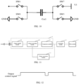
- the charge transfer module 11 includes a first switch SW1, a second switch SW2 and a first power supply V1.
- the first power supply V1 is connected to a first terminal of the first switch SW1, a second terminal of the first switch SW1 is connected to a first terminal of the second switch SW2, a second terminal of the second switch SW2 is grounded (GND), a connection between the first switch SW1 and the second switch SW2 is connected to a first terminal of a capacitor C x to be detected, a second terminal of the capacitor C x to be detected is connected to a voltage conversion module 12, and a control terminal of the first switch SW1 and a control terminal of the second switch SW2 are respectively configured to receive a driving signal (not shown in the figure).
- the driving signal is a signal sent by a signal generator, which may be a RC oscillator, a processor, a crystal oscillator circuit, and the like.
- the first switch SW1 is configured to be closed when the capacitor C x to be detected is discharged and be opened when the capacitor C x to be detected is charged.
- the second switch SW2 is configured to be opened when the capacitor C x to be detected is discharged and be closed when the capacitor C x to be detected is discharged.
- the driving signal may be a clock signal.
- the first switch SW1 is closed in response to the driving signal being at a high level and is opened in response to the driving signal being at a low level.
- the second switch SW2 is opened in response to the driving signal being at the high level and is closed in response to the driving signal being at the low level.
- the first switch SW1 is opened and the second switch SW2 is closed in response to the driving signal being at the high level.
- the capacitor C x to be detected is connected to GND, and the charges in the capacitor C x to be detected are completely released, thus the amount of charges is 0.
- the charge transfer module 11 is applied to a self-capacitance detection mode.
- the charge transfer module 11 includes a third switch SW3, a fourth switch SW4 and a second power supply V2.
- the second power supply V2 is connected to a first terminal of the third switch SW3, a second terminal of the third switch SW3 is connected to a first terminal of the fourth switch SW4, a second terminal of the fourth switch SW4 is connected to the voltage conversion module 12, a connection between the third switch SW3 and the fourth switch SW4 is connected to a first terminal of the capacitor C x to be detected, a second terminal of the capacitor C x to be detected is grounded, and a control terminal of the third switch SW3 and a control terminal of the fourth switch SW4 are respectively configured to receive a driving signal.
- the third switch SW3 is configured to be opened when the capacitor to be detected is discharged and be closed when the capacitor C x to be detected is charged.
- the fourth switch SW4 is configured to be closed when the capacitor to be detected is discharged and be opened when the capacitor C x to be detected is charged.
- the driving signal may also be a clock signal.
- the third switch SW3 is closed in response to the driving signal being at a high level and is opened in response to the driving signal being at a low level.
- the fourth switch SW4 is opened in response to the driving signal being at the high level and is closed in response to the driving signal being at the low level.
- the third switch SW3 is closed and the fourth switch SW4 is opened in response to the driving signal being at the high level.
- the third switch SW3 is opened and the fourth switch SW4 is closed, and the capacitor C x to be detected is connected to GND. All the charges in the capacitor C x to be detected are released, thus the amount of charges is 0.
- the voltage conversion module 12 includes an operational amplifier AMP, a first reference capacitor C ref1 and a fifth switch SW5.
- the charge transfer module 11 and the charge conversion module 2 are respectively connected to an inverting input of the operational amplifier AMP.
- a non-inverting input of the operational amplifier AMP is grounded (GND).
- Two terminals of the first reference capacitor C ref1 are respectively connected to the inverting input of the operational amplifier AMP and an output of the operational amplifier AMP.
- Two terminals of the fifth switch SW5 are respectively connected to the two terminals of the first reference capacitor C ref1 , and a control terminal of the fifth switch SW5 is configured to receive a reset signal.
- the fifth switch SW5 is configured to keep being closed within a preset duration when receiving the reset signal. Specifically, referring to a waveform diagram of the reset signal in FIG. 4 , the reset signal is input into the fifth switch SW5 before the capacitance detection circuit detects the capacitor C x to be detected. In response to the reset signal being at a high level, the fifth switch SW5 is closed. A duration of the reset signal being at the high level is regarded as the preset duration, and the fifth switch SW5 may be kept being closed within the preset duration, so that all the charges at the two terminals of the first reference capacitor C ref1 may be released. In response to the reset signal being at a low level, the fifth switch SW5 may be opened, so that the fifth switch SW5 is opened after the preset duration, and then the capacitance detection circuit may detect the capacitor C x to be detected.
- the charge transfer of the capacitor C x to be detected is performed for multiple times.
- the amount of charges received by the operational amplifier AMP is represented by Q accumulate below.
- V out Q accumulate /C ref1 .
- an output of the comparison module 13 is 0.
- the output voltage V out of the operational amplifier AMP gradually increases until the V out is greater than the preset voltage threshold V x in the comparison module 13.
- the output of the comparison module 13 changes from 0 to 1.
- the function of the voltage conversion module is realized by a circuit shown in FIG. 6 , but the invention is not limited to such exemplification.
- the voltage conversion module 12 includes a summation submodule 121, an integration submodule 122 and a conversion submodule 123 which are connected in sequence, and the summation submodule 121 is connected to the charge transfer module 11 and the charge conversion module 2 respectively.
- the summation submodule 121 is configured to calculate an algebraic sum of received charges
- the integration submodule 122 is configured to capture and sum the charges output by the summation submodule 121
- the conversion submodule 123 is configured to convert the charges output by the integration submodule 122 into an analog voltage signal.
- the comparison module 13 includes a voltage comparator 131 and a first trigger 132.
- the first trigger 132 may be a D trigger (which is taken as an example in the figure).
- a non-inverting input of the voltage comparator 131 is connected to the voltage conversion module 12, and an inverting input of the voltage comparator 131 is grounded (GND).
- An output of the voltage comparator 131 is connected to a first input of the first trigger 132, a second input of the first trigger 132 is configured to receive a driving signal, and an output of the first trigger 132 is connected to the filter module 3.
- the driving signal may be the clock signal shown in FIG. 4 .
- the voltage comparator 131 is configured to output a high level in response to a voltage value of the analog voltage signal being greater than a voltage threshold, and output a low level in response to the voltage value of the analog voltage signal being less than the voltage threshold.
- the first trigger 132 is configured to output a current level of the voltage comparator 131 as a level of the digital voltage signal in response to the driving signal being at a rising edge, and keep the level of the output digital voltage signal unchanged in response to the driving signal being at a falling edge. That is, the first trigger 132 takes the current level of the voltage comparator 131 as the level of the output digital voltage signal in response to the driving signal being at a high level, and the first trigger 132 keeps the level of the output digital voltage signal unchanged in response to the driving signal being at a low level.
- this embodiment provides specific structures of the charge transfer module, the voltage conversion module and the comparison module in the capacitance detection circuit.
- a third embodiment of the present disclosure relates to a capacitance detection circuit. Compared with the second embodiment, the main difference of this embodiment is that a specific structure of a charge conversion module is provided.
- a charge conversion module 2 includes a logic controller 21 and a charge output submodule 22.
- a first terminal of the logic controller 21 is connected to a comparison module 13, and a second terminal of the logic controller 21 is connected to a voltage conversion module 12 through the charge output submodule 22.
- the logic controller 21 In response to a digital voltage signal being at a high level, the logic controller 21 is configured to control the charge output submodule 22 to output negative charges with a preset charge amount to the voltage conversion module 12.
- the charge output submodule 22 includes a sixth switch SW6, a seventh switch SW7, an eighth switch SW8, a ninth switch SW9, a third power supply V3 and a second reference capacitor C ref2 .
- a first terminal of the sixth switch SW6 is connected to the voltage conversion module 12, a second terminal of the sixth switch SW6 is connected to a first terminal of the eighth switch SW8, a second terminal of the eighth switch SW8 is grounded, a connection between the sixth switch SW6 and the eighth switch SW8 is connected to a first terminal of the second reference capacitor C ref2 .
- a first terminal of the seventh switch SW7 is connected to the third power supply V3, a second terminal of the seventh switch SW7 is connected to a first terminal of the ninth switch SW9, a second terminal of the ninth switch SW9 is grounded, and a connection between the seventh switch SW7 and the ninth switch SW9 is connected to a second terminal of the second reference capacitor C ref2 .
- a control terminal of the sixth switch SW6, a control terminal of the seventh switch SW7, a control terminal of the eighth switch SW8 and a control terminal of the ninth switch SW9 are respectively connected to the logic controller 21.
- the logic controller 21 is configured to control the sixth switch SW6 and the ninth switch SW9 to be opened and control the seventh switch SW7 and the eighth switch SW8 to be closed.
- the second reference capacitor C ref2 is connected to the third power supply V3 and is charged to a reference voltage V ref2 .
- the logic controller 21 is configured to control the sixth switch SW6 and the ninth switch SW9 to be closed and control the seventh switch SW7 and the eighth switch SW8 to be opened.
- the second reference capacitor C ref2 is grounded (GND), and all the charges stored in the second reference capacitor C ref2 are released to the ground.
- this embodiment provides a specific structure of the charge conversion module.
- a fourth embodiment of the present disclosure relates to a capacitance detection circuit. Compared with the first embodiment, the main difference of this embodiment is that, referring to FIG. 11 , the capacitance detection circuit further includes an extraction module 4. A comparison module 13 is connected to a filter module 3 through the extraction module 4.
- the extraction module 4 is configured to output a digital voltage signal within a preset time period to the filter module 3.
- the extraction module 4 is an AND circuit.
- a first input of the AND circuit is connected to the comparison module 13, and an output of the AND circuit is connected to the filter module 3.
- a second input of the AND circuit is configured to receive an output control signal, and a duration of the output control signal at a high level in one cycle is designated as the preset time period. That is, referring to FIG. 12 , the output control signal is a periodic signal, which is at a high level within a preset time period T in one cycle of the output control signal, so that the digital voltage signal in the preset time period T may be extracted and input into the filter module 3.
- the filter module 3 may obtain a value representing a capacitance of a capacitor to be detected in this cycle according to the digital voltage signal in the preset time period T. Thus, the value of the capacitance of the capacitor C x to be detected may be obtained periodically.
- the filter module 3 includes a counter 31 and a second trigger 32.
- the second trigger 32 may be a D trigger.
- the comparison module 13 is connected to an input of the counter 31, an output of the counter 31 is connected to a first input of the second trigger 32, and a second input of the second trigger 32 is configured to receive an output control signal (as shown in FIG. 12 ).
- a driving terminal of the counter 31 is configured to receive a driving signal (as shown in FIG. 4 ). In response to that the driving signal is at a rising edge and the digital voltage signal is at a high level, the counter 31 is configured to add 1 to a current count value.
- the second trigger 32 is configured to output the count value of the counter 31 as the value representing the capacitance of the capacitor C x to be detected.
- the counter 31 counts in response to the driving signal being at the high level, adds 1 to the count value in response to the digital voltage signal being at the high level, and keeps the count value unchanged in response to the digital voltage signal being at a low level.
- the second trigger 32 outputs the count value accumulated by the counter 31 as the value representing the capacitance of the capacitor C x to be detected, and clears the count value of the counter 31.
- the extraction module is added into the capacitance detection circuit in this embodiment, so that the capacitor to be detected may be periodically detected, thereby reducing the power consumption.
- a fifth embodiment of the present disclosure relates to a sensor.
- the sensor may be a capacitance sensor, and the sensor may be applied in an electronic device.
- the sensor includes the capacitance detection circuit provided in any one of the first to fourth embodiments.
- a sixth embodiment of the present disclosure relates to a chip.
- the chip may be a capacitance detection chip, and the chip may be applied in an electronic device.
- the chip includes the capacitance detection circuit provided in any one of the first to fourth embodiments.
- a seventh embodiment of the present disclosure relates to an electronic device including the capacitance detection circuit provided in any one of the first to fourth embodiments.
- the electronic device may be, for example, a mobile phone, a tablet PC, and the like.
- the electronic device further includes a processor, which is configured to obtain a capacitance of a capacitor to be detected according to a value representing the capacitance of the capacitor to be detected which is output by the capacitance detection circuit.
- the capacitance of the capacitor C x to be detected is obtained according to a preset measurement range of the capacitance detection circuit.
- the measurement range of the capacitance detection circuit is 0 to 10 pF
Landscapes
- Physics & Mathematics (AREA)
- General Physics & Mathematics (AREA)
- Engineering & Computer Science (AREA)
- General Engineering & Computer Science (AREA)
- Theoretical Computer Science (AREA)
- Mathematical Physics (AREA)
- Human Computer Interaction (AREA)
- Measurement Of Resistance Or Impedance (AREA)
- Analogue/Digital Conversion (AREA)
Claims (10)
- Circuit de détection de capacité comprenant :un module de commande de capacité (1), un module de conversion de charge (2) et un module de filtrage (3) qui sont connectés entre eux ;dans lequel le module de commande de capacité (1) est configuré pour commander un condensateur à détecter (Cx) pour se charger et se décharger plusieurs fois, et générer un signal de tension numérique selon une quantité de charges reçues ; dans lequel le condensateur à détecter (Cx) libère toutes les charges stockées après avoir été chargé à une tension prédéfinie au cours de chaque charge et décharge ;en réponse à un signal de tension numérique de niveau élevé, le module de conversion de charge (2) est configuré pour délivrer des charges négatives avec une quantité de charge prédéfinie au module de commande de capacité (1), dans lequel la quantité de charge prédéfinie est supérieure ou égale à une quantité de charges stockées lorsque le condensateur à détecter (Cx) est chargé à la tension prédéfinie ; etle module de filtrage (3) est configuré pour obtenir une valeur représentant une capacité du condensateur à détecter (Cx) selon le signal de tension numérique généré après que le condensateur à détecter (Cx) a été chargé et déchargé plusieurs fois ;dans lequel le module de commande de capacité (1) comprend un module de transfert de charge (11), un module de conversion de tension (12) et un module de comparaison (13) qui sont connectés en séquence ; dans lequel le module de comparaison (13) est connecté au module de filtrage (3), et le module de conversion de charge (2) est connecté au module de conversion de tension (12) ;dans lequel le module de transfert de charge (11) est configuré pour commander le condensateur à détecter (Cx) pour se charger et se décharger plusieurs fois, dans lequel le condensateur à détecter (Cx) libère toutes les charges stockées vers le module de conversion de tension (12) après avoir été chargé à la tension prédéfinie au cours de chaque charge et décharge ;le module de conversion de tension (12) est configuré pour convertir toutes les charges stockées qui sont reçues en un signal de tension analogique ;le module de comparaison (13) est configuré pour délivrer le signal de tension numérique selon un seuil de tension prédéfini et le signal de tension analogique ; eten réponse à un signal de tension numérique de niveau élevé, le module de conversion de charge (2) est configuré pour délivrer les charges négatives avec la quantité de charge prédéfinie au module de conversion de tension (12) ;caractérisé en ce quele module de comparaison (13) comprend un comparateur de tensions (131) et un premier déclencheur (132) ;dans lequel une entrée non-inverseuse du comparateur de tensions (131) est connectée au module de conversion de tension (12), une entrée inverseuse du comparateur de tensions (131) est mise à la terre, une sortie du comparateur de tensions (131) est connectée à une première entrée du premier déclencheur (132), une deuxième entrée du premier déclencheur (132) est configurée pour recevoir un signal de commande de sortie, une troisième entrée du premier déclencheur (132) est configurée pour recevoir un signal d'excitation, et une sortie du premier déclencheur (132) est connectée au module de filtrage (3) ;en réponse à une valeur de tension du signal de tension analogique supérieure au seuil de tension, le comparateur de tensions (131) est configuré pour délivrer un niveau élevé, et en réponse à une valeur de tension du signal de tension analogique inférieure au seuil de tension, le comparateur de tensions (131) est configuré pour délivrer un niveau bas ; eten réponse à un signal d'excitation de front montant, le premier déclencheur (132) est configuré pour délivrer un niveau de courant du comparateur de tensions (131) en tant que niveau du signal de tension numérique, et en réponse à un signal d'excitation de front descendant, le premier déclencheur (132) est configuré pour garder inchangé le niveau du signal de tension numérique.
- Circuit de détection de capacité selon la revendication 1, dans lequel le module de transfert de charge (11) comprend un premier commutateur (SW1), un deuxième commutateur (SW2) et une première alimentation électrique (V1) ;dans lequel la première alimentation électrique (V1) est connectée à une première borne du premier commutateur (SW1), une deuxième borne du premier commutateur (SW1) est connectée à une première borne du deuxième commutateur (SW2), une deuxième borne du deuxième commutateur (SW2) est mise à la terre, une connexion entre le premier commutateur (SW1) et le deuxième commutateur (SW2) est connectée à une première borne du condensateur à détecter (Cx), une deuxième borne du condensateur à détecter (Cx) est connectée au module de conversion de tension (12), et une borne de commande du premier commutateur (SW1) et une borne de commande du deuxième commutateur (SW2) sont respectivement configurées pour recevoir un signal d'excitation ;en réponse au signal d'excitation, le premier commutateur (SW1) est configuré pour être fermé lorsque le condensateur à détecter (Cx) est chargé, et pour être ouvert lorsque le condensateur à détecter (Cx) est déchargé ; eten réponse au signal d'excitation, le deuxième commutateur (SW2) est configuré pour être ouvert lorsque le condensateur à détecter (Cx) est chargé, et pour être fermé lorsque le condensateur à détecter (Cx) est déchargé.
- Circuit de détection de capacité selon la revendication 1, dans lequel le module de transfert de charge (1) comprend un troisième commutateur (SW3), un quatrième commutateur (SW4) et une deuxième alimentation électrique (V2) ;dans lequel la deuxième alimentation électrique (V2) est connectée à une première borne du troisième commutateur (SW3), une deuxième borne du troisième commutateur (SW3) est connectée à une première borne du quatrième commutateur (SW4), une deuxième borne du quatrième commutateur (SW4) est connectée au module de conversion de tension (12), une connexion entre le troisième commutateur (SW3) et le quatrième commutateur (SW4) est connectée à une première borne du condensateur à détecter (Cx), une deuxième borne du condensateur à détecter (Cx) est mise à la terre, et une borne de commande du troisième commutateur (SW3) et une borne de commande du quatrième commutateur (SW4) sont respectivement configurées pour recevoir un signal d'excitation ;en réponse au signal d'excitation, le troisième commutateur (SW3) est configuré pour être ouvert lorsque le condensateur à détecter (Cx) est déchargé, et pour être fermé lorsque le condensateur à détecter (Cx) est chargé ; eten réponse au signal d'excitation, le quatrième commutateur (SW4) est configuré pour être fermé lorsque le condensateur à détecter (Cx) est déchargé, et pour être ouvert lorsque le condensateur à détecter (Cx) est chargé.
- Circuit de détection de capacité selon la revendication 1, dans lequel le module de conversion de tension (12) comprend un amplificateur opérationnel (AMP), un premier condensateur de référence (Cref1) et un cinquième commutateur (SW5) ;dans lequel le module de transfert de charge (11) et le module de conversion de charge (2) sont respectivement connectés à une entrée inverseuse de l'amplificateur opérationnel (AMP), une entrée non-inverseuse de l'amplificateur opérationnel (AMP) est mise à la terre, deux bornes du premier condensateur de référence (Cref1) sont respectivement connectées à l'entrée inverseuse de l'amplificateur opérationnel (AMP) et à une sortie de l'amplificateur opérationnel (AMP), deux bornes du cinquième commutateur (SW5) sont respectivement connectées aux deux bornes du premier condensateur de référence (Cref1), et une borne de commande du cinquième commutateur (SW5) est configurée pour recevoir un signal de réinitialisation ; eten réponse au signal de réinitialisation, le cinquième commutateur (SW5) est configuré pour rester fermé pendant une durée prédéfinie avant que le module de transfert de charge (11) ne commande le condensateur à détecter (Cx) pour se charger et se décharger plusieurs fois.
- Circuit de détection de capacité selon la revendication 1, dans lequel le module de conversion de charge (2) comprend un dispositif de commande logique (21) et un sous-module de sortie de charge (22), une première borne du dispositif de commande logique (21) est connectée au module de comparaison (13), et une deuxième borne du dispositif de commande logique (21) est connectée au module de conversion de tension (12) par le sous-module de sortie de charge (22) ;
dans lequel, en réponse à un signal de tension numérique de niveau élevé, le dispositif de commande logique (21) est configuré pour commander le sous-module de sortie de charge (22) pour délivrer les charges négatives avec le quantité de charge prédéfinie au module de conversion de tension (12). - Circuit de détection de capacité selon la revendication 5, dans lequel le sous-module de sortie de charge (22) comprend un sixième commutateur (SW6), un septième commutateur (SW7), un huitième commutateur (SW8), un neuvième commutateur (SW9), une troisième alimentation électrique (V3) et un deuxième condensateur de référence (Cref2) ;dans lequel une première borne du sixième commutateur (SW6) est connectée au module de conversion de tension (12), une deuxième borne du sixième commutateur (SW6) est connectée à une première borne du huitième commutateur (SW8), une deuxième borne du huitième commutateur (SW8) est mise à la terre, une connexion entre le sixième commutateur (SW6) et le huitième commutateur (SW8) est connectée à une première borne du deuxième condensateur de référence (Cref2), une première borne du septième commutateur (SW7) est connectée à la troisième alimentation électrique (V3), une deuxième borne du septième commutateur (SW7) est connectée à une première borne du neuvième commutateur (SW9), une deuxième borne du neuvième commutateur (SW9) est mise à la terre, et une connexion entre le septième commutateur (SW7) et le neuvième commutateur (SW9) est connectée à une deuxième borne du deuxième condensateur de référence (Cref2) ;une borne de commande du sixième commutateur (SW6), une borne de commande du septième commutateur (SW7), une borne de commande du huitième commutateur (SW8) et une borne de commande du neuvième commutateur (SW9) sont respectivement connectées au dispositif de commande logique (21) ;en réponse à un signal de tension numérique de niveau bas, le dispositif de commande logique (21) est configuré pour commander la fermeture du sixième commutateur (SW6) et du neuvième commutateur (SW9), et commander l'ouverture du septième commutateur (SW7) et du huitième commutateur (SW8) ; eten réponse à un signal de tension numérique de niveau élevé, le dispositif de commande logique (21) est configuré pour commander l'ouverture du sixième commutateur (SW6) et du neuvième commutateur (SW9), et commander la fermeture du septième commutateur (SW7) et du huitième commutateur (SW8).
- Capteur, comprenant le circuit de détection de capacité selon l'une des revendications 1 à 6.
- Puce comprenant le circuit de détection de capacité selon l'une des revendications 1 à 6.
- Dispositif électronique, comprenant le circuit de détection de capacité selon l'une des revendications 1 à 6.
- Dispositif électronique selon la revendication 9, dans lequel le dispositif électronique comprend en outre un processeur ;
dans lequel le processeur est configuré pour obtenir la capacité du condensateur à détecter (Cx) selon la valeur représentant la capacité du condensateur à détecter (Cx) émise par le circuit de détection de capacité.
Applications Claiming Priority (1)
| Application Number | Priority Date | Filing Date | Title |
|---|---|---|---|
| PCT/CN2020/077661 WO2021174428A1 (fr) | 2020-03-03 | 2020-03-03 | Circuit de détection de condensateur, capteur, puce et dispositif électronique |
Publications (3)
| Publication Number | Publication Date |
|---|---|
| EP4080227A1 EP4080227A1 (fr) | 2022-10-26 |
| EP4080227A4 EP4080227A4 (fr) | 2023-03-29 |
| EP4080227B1 true EP4080227B1 (fr) | 2024-11-27 |
Family
ID=72859240
Family Applications (1)
| Application Number | Title | Priority Date | Filing Date |
|---|---|---|---|
| EP20922556.4A Active EP4080227B1 (fr) | 2020-03-03 | 2020-03-03 | Circuit de détection de condensateur, capteur, puce et dispositif électronique |
Country Status (5)
| Country | Link |
|---|---|
| US (1) | US11609664B2 (fr) |
| EP (1) | EP4080227B1 (fr) |
| KR (1) | KR102623568B1 (fr) |
| CN (1) | CN111819451B (fr) |
| WO (1) | WO2021174428A1 (fr) |
Families Citing this family (14)
| Publication number | Priority date | Publication date | Assignee | Title |
|---|---|---|---|---|
| WO2022174728A1 (fr) * | 2021-02-22 | 2022-08-25 | 珠海迈巨微电子有限责任公司 | Appareil de détection de déformation de batterie et système de gestion de batterie |
| CN113447697B (zh) * | 2021-04-19 | 2022-11-08 | 深圳市爱协生科技有限公司 | 信号检测电路、信号检测方法、触摸面板及显示装置 |
| CN114640335A (zh) * | 2022-05-09 | 2022-06-17 | 深圳市航顺芯片技术研发有限公司 | 一种按键防水电路、按键以及电子设备 |
| CN114964318B (zh) * | 2022-05-24 | 2025-01-28 | 哈尔滨工业大学 | 一种带有自校准功能的非同步电容传感器接口电路 |
| CN115343515B (zh) * | 2022-10-17 | 2023-03-07 | 基合半导体(宁波)有限公司 | 模拟前端电路、电容测量电路、芯片及电子设备 |
| WO2024164163A1 (fr) * | 2023-02-08 | 2024-08-15 | 深圳市汇顶科技股份有限公司 | Circuit d'attaque, appareil de commande tactile et dispositif électronique |
| CN115601795B (zh) * | 2022-12-05 | 2023-04-21 | 深圳市汇顶科技股份有限公司 | 电容指纹检测电路、电容指纹检测装置和电子设备 |
| CN116506879B (zh) * | 2023-04-24 | 2025-09-26 | 深圳市酷开网络科技股份有限公司 | 一种wifi老化掉线处理方法、装置 |
| CN116840570B (zh) * | 2023-06-30 | 2025-03-07 | 思瑞浦微电子科技(上海)有限责任公司 | 伪差分电容检测电路及检测方法 |
| CN117665381B (zh) * | 2024-01-31 | 2024-05-24 | 荣耀终端有限公司 | 检测电路、电子设备和方法 |
| CN118707195B (zh) * | 2024-08-30 | 2025-02-11 | 杭州米芯微电子有限公司 | 一种电容测量方法及电容测量电路 |
| CN119471062A (zh) * | 2024-11-12 | 2025-02-18 | 无锡英迪芯微电子科技股份有限公司 | 一种电容检测电路和检测设备 |
| CN119763648B (zh) * | 2024-12-20 | 2025-09-30 | 深圳市德明利技术股份有限公司 | 电容阈值的测试方法、装置及电子设备 |
| CN119804999B (zh) * | 2025-03-12 | 2025-06-17 | 成都维客昕微电子有限公司 | 一种电容检测电路、方法及设备 |
Family Cites Families (34)
| Publication number | Priority date | Publication date | Assignee | Title |
|---|---|---|---|---|
| US5576628A (en) * | 1994-09-30 | 1996-11-19 | Telcom Semiconductor, Inc. | Method and apparatus to measure capacitance |
| JP4363281B2 (ja) * | 2004-09-08 | 2009-11-11 | オムロン株式会社 | 容量計測装置および方法、並びにプログラム |
| CN101315398B (zh) * | 2007-05-28 | 2011-03-23 | 承永资讯科技股份有限公司 | 电容值测量装置及方法 |
| TWI361280B (en) * | 2008-07-18 | 2012-04-01 | Raydium Semiconductor Corp | Evaluation circuit for capacitance and method thereof |
| CN101738544B (zh) * | 2008-11-17 | 2012-08-22 | 瑞鼎科技股份有限公司 | 电容测量电路及其电容测量方法 |
| JP2010152876A (ja) * | 2008-11-26 | 2010-07-08 | Seiko Instruments Inc | 静電検出装置、静電検出回路、静電検出方法及び初期化方法 |
| US8866499B2 (en) * | 2009-08-27 | 2014-10-21 | Analog Devices, Inc. | System and method for measuring capacitance |
| TWI409683B (zh) * | 2010-02-04 | 2013-09-21 | Chunghwa Picture Tubes Ltd | 觸控面板偵測電路 |
| US8854107B2 (en) * | 2010-05-04 | 2014-10-07 | Zinitix Co., Ltd. | Integrator circuit with inverting integrator and non-inverting integrator |
| TWI410853B (zh) * | 2010-05-07 | 2013-10-01 | Novatek Microelectronics Corp | 用於觸控裝置之電容量測量裝置 |
| CN102253289B (zh) * | 2010-05-18 | 2013-12-25 | 联咏科技股份有限公司 | 用于触控装置的电容量测量装置 |
| KR101388906B1 (ko) * | 2012-05-30 | 2014-04-23 | 삼성전기주식회사 | 정전용량 감지 장치, 정전용량 감지 방법, 및 터치스크린 장치 |
| JP6043679B2 (ja) * | 2012-08-01 | 2016-12-14 | アルプス電気株式会社 | 静電容量検出回路及び入力デバイス |
| US9459833B2 (en) * | 2012-09-28 | 2016-10-04 | Maxim Integrated Products, Inc. | System and method with specific ordered execution over physical elements |
| US8982093B2 (en) * | 2012-12-20 | 2015-03-17 | Broadcom Corporation | Capacitive touch sensing system with interference rejection |
| CN106055183B (zh) * | 2012-12-30 | 2019-11-08 | 比亚迪股份有限公司 | 电容检测电路 |
| CN203084695U (zh) * | 2012-12-31 | 2013-07-24 | 比亚迪股份有限公司 | 电容检测电路 |
| CN203117298U (zh) * | 2013-01-30 | 2013-08-07 | 比亚迪股份有限公司 | 一种电容检测电路 |
| JP6400944B2 (ja) * | 2014-05-26 | 2018-10-03 | シナプティクス・ジャパン合同会社 | 容量検出回路、タッチ検出回路及びそれを備える半導体集積回路 |
| US10317250B2 (en) * | 2015-01-16 | 2019-06-11 | Ion Geophysical Corporation | Direct coupling of a capacitive sensor to a delta-sigma converter |
| CN106325632B (zh) * | 2015-06-15 | 2020-12-15 | 恩智浦美国有限公司 | 具有噪声抑制的电容传感器 |
| CN105116232B (zh) * | 2015-08-13 | 2019-03-01 | 上海矽睿科技有限公司 | 一种电容检测电路及电容传感电路 |
| CN106775141B (zh) * | 2015-12-30 | 2019-09-27 | 深圳市汇顶科技股份有限公司 | 电容感测电路及触控面板 |
| CN107466368B (zh) * | 2016-03-29 | 2019-05-31 | 深圳市汇顶科技股份有限公司 | 便携式电子设备、电容触摸屏和电容检测电路 |
| CN108139840A (zh) * | 2016-05-17 | 2018-06-08 | 深圳市汇顶科技股份有限公司 | 电容检测的装置 |
| TWI621984B (zh) * | 2016-12-02 | 2018-04-21 | 瑞鼎科技股份有限公司 | 電容値量測電路及電容値量測方法 |
| CN106501618B (zh) * | 2016-12-30 | 2019-02-26 | 上海东软载波微电子有限公司 | 电容容值测量电路 |
| US10656191B2 (en) * | 2017-12-18 | 2020-05-19 | Microsoft Technology Licensing, Llc | Capacitance measuring circuit |
| CN109496273B (zh) * | 2018-01-24 | 2021-05-11 | 深圳市汇顶科技股份有限公司 | 电容检测电路、触摸检测装置和终端设备 |
| CN110300897B (zh) * | 2018-01-24 | 2020-11-03 | 深圳市汇顶科技股份有限公司 | 电容检测电路、触控装置和终端设备 |
| EP3617720B1 (fr) * | 2018-06-21 | 2021-12-01 | Shenzhen Goodix Technology Co., Ltd. | Dispositif tactile et dispositif terminal |
| WO2020237503A1 (fr) | 2019-05-28 | 2020-12-03 | 深圳市汇顶科技股份有限公司 | Circuit de détection de capacité, procédé de détection de capacité, puce tactile et dispositif électronique |
| WO2021097727A1 (fr) | 2019-11-20 | 2021-05-27 | 深圳市汇顶科技股份有限公司 | Circuit de mesure de capacité, appareil tactile, dispositif terminal et procédé de mesure de capacité |
| CN211375581U (zh) * | 2019-11-20 | 2020-08-28 | 深圳市汇顶科技股份有限公司 | 一种电容检测电路、触控装置、终端设备 |
-
2020
- 2020-03-03 KR KR1020217031383A patent/KR102623568B1/ko active Active
- 2020-03-03 EP EP20922556.4A patent/EP4080227B1/fr active Active
- 2020-03-03 CN CN202080001590.3A patent/CN111819451B/zh active Active
- 2020-03-03 WO PCT/CN2020/077661 patent/WO2021174428A1/fr not_active Ceased
-
2021
- 2021-09-28 US US17/488,280 patent/US11609664B2/en active Active
Also Published As
| Publication number | Publication date |
|---|---|
| US20220035470A1 (en) | 2022-02-03 |
| CN111819451A (zh) | 2020-10-23 |
| EP4080227A1 (fr) | 2022-10-26 |
| EP4080227A4 (fr) | 2023-03-29 |
| US11609664B2 (en) | 2023-03-21 |
| KR102623568B1 (ko) | 2024-01-11 |
| KR20210133284A (ko) | 2021-11-05 |
| WO2021174428A1 (fr) | 2021-09-10 |
| CN111819451B (zh) | 2023-06-09 |
Similar Documents
| Publication | Publication Date | Title |
|---|---|---|
| EP4080227B1 (fr) | Circuit de détection de condensateur, capteur, puce et dispositif électronique | |
| EP3008824B1 (fr) | Détection de proximité capacitive utilisant la conversion delta-sigma | |
| EP3543668B1 (fr) | Circuit de détection de capacité, appareil de détection tactile et dispositif terminal | |
| CN105046194B (zh) | 一种包含积分器的电容指纹传感器 | |
| CN208013309U (zh) | 电容检测电路、触控装置和终端设备 | |
| US20090225044A1 (en) | Determining touch on keys of touch sensitive input device | |
| US20110068810A1 (en) | Sensing method and driving circuit of capacitive touch screen | |
| US20160003881A1 (en) | Capacitance sensing circuits and methods | |
| EP3324331B1 (fr) | Circuit de détection capacitif | |
| CN109039319B (zh) | 一种抗干扰的电容式触摸按键控制器及实现方法 | |
| CN101685364B (zh) | 触摸面板的传感装置及方法 | |
| CN101477152A (zh) | 一种电容检测装置及方法 | |
| US7750612B2 (en) | Voltage-pulse converting circuit and charge control system | |
| CN111900782B (zh) | 充电控制电路、充电芯片及充电设备 | |
| US20030179123A1 (en) | Analog-to-digital conversion using a counter | |
| JP2022082500A (ja) | 圧力検出回路、装置及び圧力入力装置 | |
| CN112514261B (zh) | 光-数字转换器装置和用于光-数字转换的方法 | |
| US20100052741A1 (en) | Dual integrator circuit for analog front end (afe) | |
| CN213937865U (zh) | 快速乒乓式互电容转换电路 | |
| CN101135720B (zh) | 检测电池电量系统及其手持式电子装置 | |
| CN212872665U (zh) | 电容变化检测电路 | |
| CN2938571Y (zh) | 电荷转移装置、触摸感应装置 | |
| US8253615B2 (en) | Current sensing circuit | |
| KR102081155B1 (ko) | 고정밀도의 저전력 센서인터페이스장치 | |
| CN101369812B (zh) | 具交流电源免疫能力的触碰电容式传感器 |
Legal Events
| Date | Code | Title | Description |
|---|---|---|---|
| STAA | Information on the status of an ep patent application or granted ep patent |
Free format text: STATUS: THE INTERNATIONAL PUBLICATION HAS BEEN MADE |
|
| PUAI | Public reference made under article 153(3) epc to a published international application that has entered the european phase |
Free format text: ORIGINAL CODE: 0009012 |
|
| STAA | Information on the status of an ep patent application or granted ep patent |
Free format text: STATUS: REQUEST FOR EXAMINATION WAS MADE |
|
| 17P | Request for examination filed |
Effective date: 20210928 |
|
| AK | Designated contracting states |
Kind code of ref document: A1 Designated state(s): AL AT BE BG CH CY CZ DE DK EE ES FI FR GB GR HR HU IE IS IT LI LT LU LV MC MK MT NL NO PL PT RO RS SE SI SK SM TR |
|
| A4 | Supplementary search report drawn up and despatched |
Effective date: 20230301 |
|
| RIC1 | Information provided on ipc code assigned before grant |
Ipc: H03K 17/96 20060101ALI20230223BHEP Ipc: G01D 5/24 20060101ALI20230223BHEP Ipc: G01R 27/26 20060101AFI20230223BHEP |
|
| DAV | Request for validation of the european patent (deleted) | ||
| DAX | Request for extension of the european patent (deleted) | ||
| STAA | Information on the status of an ep patent application or granted ep patent |
Free format text: STATUS: EXAMINATION IS IN PROGRESS |
|
| 17Q | First examination report despatched |
Effective date: 20231128 |
|
| GRAP | Despatch of communication of intention to grant a patent |
Free format text: ORIGINAL CODE: EPIDOSNIGR1 |
|
| STAA | Information on the status of an ep patent application or granted ep patent |
Free format text: STATUS: GRANT OF PATENT IS INTENDED |
|
| INTG | Intention to grant announced |
Effective date: 20240605 |
|
| GRAS | Grant fee paid |
Free format text: ORIGINAL CODE: EPIDOSNIGR3 |
|
| GRAA | (expected) grant |
Free format text: ORIGINAL CODE: 0009210 |
|
| STAA | Information on the status of an ep patent application or granted ep patent |
Free format text: STATUS: THE PATENT HAS BEEN GRANTED |
|
| AK | Designated contracting states |
Kind code of ref document: B1 Designated state(s): AL AT BE BG CH CY CZ DE DK EE ES FI FR GB GR HR HU IE IS IT LI LT LU LV MC MK MT NL NO PL PT RO RS SE SI SK SM TR |
|
| REG | Reference to a national code |
Ref country code: GB Ref legal event code: FG4D |
|
| REG | Reference to a national code |
Ref country code: CH Ref legal event code: EP |
|
| REG | Reference to a national code |
Ref country code: IE Ref legal event code: FG4D |
|
| REG | Reference to a national code |
Ref country code: DE Ref legal event code: R096 Ref document number: 602020042305 Country of ref document: DE |
|
| REG | Reference to a national code |
Ref country code: LT Ref legal event code: MG9D |
|
| REG | Reference to a national code |
Ref country code: NL Ref legal event code: MP Effective date: 20241127 |
|
| PG25 | Lapsed in a contracting state [announced via postgrant information from national office to epo] |
Ref country code: HR Free format text: LAPSE BECAUSE OF FAILURE TO SUBMIT A TRANSLATION OF THE DESCRIPTION OR TO PAY THE FEE WITHIN THE PRESCRIBED TIME-LIMIT Effective date: 20241127 Ref country code: IS Free format text: LAPSE BECAUSE OF FAILURE TO SUBMIT A TRANSLATION OF THE DESCRIPTION OR TO PAY THE FEE WITHIN THE PRESCRIBED TIME-LIMIT Effective date: 20250327 Ref country code: PT Free format text: LAPSE BECAUSE OF FAILURE TO SUBMIT A TRANSLATION OF THE DESCRIPTION OR TO PAY THE FEE WITHIN THE PRESCRIBED TIME-LIMIT Effective date: 20250327 |
|
| PG25 | Lapsed in a contracting state [announced via postgrant information from national office to epo] |
Ref country code: FI Free format text: LAPSE BECAUSE OF FAILURE TO SUBMIT A TRANSLATION OF THE DESCRIPTION OR TO PAY THE FEE WITHIN THE PRESCRIBED TIME-LIMIT Effective date: 20241127 Ref country code: NL Free format text: LAPSE BECAUSE OF FAILURE TO SUBMIT A TRANSLATION OF THE DESCRIPTION OR TO PAY THE FEE WITHIN THE PRESCRIBED TIME-LIMIT Effective date: 20241127 |
|
| REG | Reference to a national code |
Ref country code: AT Ref legal event code: MK05 Ref document number: 1746154 Country of ref document: AT Kind code of ref document: T Effective date: 20241127 |
|
| PG25 | Lapsed in a contracting state [announced via postgrant information from national office to epo] |
Ref country code: BG Free format text: LAPSE BECAUSE OF FAILURE TO SUBMIT A TRANSLATION OF THE DESCRIPTION OR TO PAY THE FEE WITHIN THE PRESCRIBED TIME-LIMIT Effective date: 20241127 |
|
| PG25 | Lapsed in a contracting state [announced via postgrant information from national office to epo] |
Ref country code: ES Free format text: LAPSE BECAUSE OF FAILURE TO SUBMIT A TRANSLATION OF THE DESCRIPTION OR TO PAY THE FEE WITHIN THE PRESCRIBED TIME-LIMIT Effective date: 20241127 |
|
| PG25 | Lapsed in a contracting state [announced via postgrant information from national office to epo] |
Ref country code: NO Free format text: LAPSE BECAUSE OF FAILURE TO SUBMIT A TRANSLATION OF THE DESCRIPTION OR TO PAY THE FEE WITHIN THE PRESCRIBED TIME-LIMIT Effective date: 20250227 |
|
| PG25 | Lapsed in a contracting state [announced via postgrant information from national office to epo] |
Ref country code: LV Free format text: LAPSE BECAUSE OF FAILURE TO SUBMIT A TRANSLATION OF THE DESCRIPTION OR TO PAY THE FEE WITHIN THE PRESCRIBED TIME-LIMIT Effective date: 20241127 Ref country code: AT Free format text: LAPSE BECAUSE OF FAILURE TO SUBMIT A TRANSLATION OF THE DESCRIPTION OR TO PAY THE FEE WITHIN THE PRESCRIBED TIME-LIMIT Effective date: 20241127 Ref country code: GR Free format text: LAPSE BECAUSE OF FAILURE TO SUBMIT A TRANSLATION OF THE DESCRIPTION OR TO PAY THE FEE WITHIN THE PRESCRIBED TIME-LIMIT Effective date: 20250228 |
|
| PG25 | Lapsed in a contracting state [announced via postgrant information from national office to epo] |
Ref country code: PL Free format text: LAPSE BECAUSE OF FAILURE TO SUBMIT A TRANSLATION OF THE DESCRIPTION OR TO PAY THE FEE WITHIN THE PRESCRIBED TIME-LIMIT Effective date: 20241127 |
|
| PG25 | Lapsed in a contracting state [announced via postgrant information from national office to epo] |
Ref country code: RS Free format text: LAPSE BECAUSE OF FAILURE TO SUBMIT A TRANSLATION OF THE DESCRIPTION OR TO PAY THE FEE WITHIN THE PRESCRIBED TIME-LIMIT Effective date: 20250227 |
|
| PG25 | Lapsed in a contracting state [announced via postgrant information from national office to epo] |
Ref country code: SM Free format text: LAPSE BECAUSE OF FAILURE TO SUBMIT A TRANSLATION OF THE DESCRIPTION OR TO PAY THE FEE WITHIN THE PRESCRIBED TIME-LIMIT Effective date: 20241127 |
|
| PG25 | Lapsed in a contracting state [announced via postgrant information from national office to epo] |
Ref country code: DK Free format text: LAPSE BECAUSE OF FAILURE TO SUBMIT A TRANSLATION OF THE DESCRIPTION OR TO PAY THE FEE WITHIN THE PRESCRIBED TIME-LIMIT Effective date: 20241127 |
|
| PG25 | Lapsed in a contracting state [announced via postgrant information from national office to epo] |
Ref country code: EE Free format text: LAPSE BECAUSE OF FAILURE TO SUBMIT A TRANSLATION OF THE DESCRIPTION OR TO PAY THE FEE WITHIN THE PRESCRIBED TIME-LIMIT Effective date: 20241127 |
|
| PG25 | Lapsed in a contracting state [announced via postgrant information from national office to epo] |
Ref country code: RO Free format text: LAPSE BECAUSE OF FAILURE TO SUBMIT A TRANSLATION OF THE DESCRIPTION OR TO PAY THE FEE WITHIN THE PRESCRIBED TIME-LIMIT Effective date: 20241127 |
|
| PG25 | Lapsed in a contracting state [announced via postgrant information from national office to epo] |
Ref country code: SK Free format text: LAPSE BECAUSE OF FAILURE TO SUBMIT A TRANSLATION OF THE DESCRIPTION OR TO PAY THE FEE WITHIN THE PRESCRIBED TIME-LIMIT Effective date: 20241127 |
|
| PG25 | Lapsed in a contracting state [announced via postgrant information from national office to epo] |
Ref country code: CZ Free format text: LAPSE BECAUSE OF FAILURE TO SUBMIT A TRANSLATION OF THE DESCRIPTION OR TO PAY THE FEE WITHIN THE PRESCRIBED TIME-LIMIT Effective date: 20241127 |
|
| PG25 | Lapsed in a contracting state [announced via postgrant information from national office to epo] |
Ref country code: IT Free format text: LAPSE BECAUSE OF FAILURE TO SUBMIT A TRANSLATION OF THE DESCRIPTION OR TO PAY THE FEE WITHIN THE PRESCRIBED TIME-LIMIT Effective date: 20241127 |
|
| REG | Reference to a national code |
Ref country code: DE Ref legal event code: R097 Ref document number: 602020042305 Country of ref document: DE |
|
| PG25 | Lapsed in a contracting state [announced via postgrant information from national office to epo] |
Ref country code: SE Free format text: LAPSE BECAUSE OF FAILURE TO SUBMIT A TRANSLATION OF THE DESCRIPTION OR TO PAY THE FEE WITHIN THE PRESCRIBED TIME-LIMIT Effective date: 20241127 |
|
| PLBE | No opposition filed within time limit |
Free format text: ORIGINAL CODE: 0009261 |
|
| STAA | Information on the status of an ep patent application or granted ep patent |
Free format text: STATUS: NO OPPOSITION FILED WITHIN TIME LIMIT |
|
| REG | Reference to a national code |
Ref country code: CH Ref legal event code: L10 Free format text: ST27 STATUS EVENT CODE: U-0-0-L10-L00 (AS PROVIDED BY THE NATIONAL OFFICE) Effective date: 20251008 |
|
| PG25 | Lapsed in a contracting state [announced via postgrant information from national office to epo] |
Ref country code: MC Free format text: LAPSE BECAUSE OF FAILURE TO SUBMIT A TRANSLATION OF THE DESCRIPTION OR TO PAY THE FEE WITHIN THE PRESCRIBED TIME-LIMIT Effective date: 20241127 |
|
| REG | Reference to a national code |
Ref country code: CH Ref legal event code: H13 Free format text: ST27 STATUS EVENT CODE: U-0-0-H10-H13 (AS PROVIDED BY THE NATIONAL OFFICE) Effective date: 20251023 |
|
| 26N | No opposition filed |
Effective date: 20250828 |
|
| PG25 | Lapsed in a contracting state [announced via postgrant information from national office to epo] |
Ref country code: LU Free format text: LAPSE BECAUSE OF NON-PAYMENT OF DUE FEES Effective date: 20250303 |
|
| REG | Reference to a national code |
Ref country code: BE Ref legal event code: MM Effective date: 20250331 |
|
| PG25 | Lapsed in a contracting state [announced via postgrant information from national office to epo] |
Ref country code: FR Free format text: LAPSE BECAUSE OF NON-PAYMENT OF DUE FEES Effective date: 20250331 |
|
| PG25 | Lapsed in a contracting state [announced via postgrant information from national office to epo] |
Ref country code: BE Free format text: LAPSE BECAUSE OF NON-PAYMENT OF DUE FEES Effective date: 20250331 |
|
| PG25 | Lapsed in a contracting state [announced via postgrant information from national office to epo] |
Ref country code: CH Free format text: LAPSE BECAUSE OF NON-PAYMENT OF DUE FEES Effective date: 20250331 |
|
| PG25 | Lapsed in a contracting state [announced via postgrant information from national office to epo] |
Ref country code: IE Free format text: LAPSE BECAUSE OF NON-PAYMENT OF DUE FEES Effective date: 20250303 |
|
| PGFP | Annual fee paid to national office [announced via postgrant information from national office to epo] |
Ref country code: GB Payment date: 20260325 Year of fee payment: 7 |
|
| PGFP | Annual fee paid to national office [announced via postgrant information from national office to epo] |
Ref country code: DE Payment date: 20260324 Year of fee payment: 7 |