EP4080263B1 - Kameramodul, abstandskomponente und verfahren zur herstellung eines kameramoduls - Google Patents
Kameramodul, abstandskomponente und verfahren zur herstellung eines kameramoduls Download PDFInfo
- Publication number
- EP4080263B1 EP4080263B1 EP20901447.1A EP20901447A EP4080263B1 EP 4080263 B1 EP4080263 B1 EP 4080263B1 EP 20901447 A EP20901447 A EP 20901447A EP 4080263 B1 EP4080263 B1 EP 4080263B1
- Authority
- EP
- European Patent Office
- Prior art keywords
- component
- mounting board
- primary
- spacer
- reference surfaces
- Prior art date
- Legal status (The legal status is an assumption and is not a legal conclusion. Google has not performed a legal analysis and makes no representation as to the accuracy of the status listed.)
- Active
Links
Images






Classifications
-
- G—PHYSICS
- G03—PHOTOGRAPHY; CINEMATOGRAPHY; ANALOGOUS TECHNIQUES USING WAVES OTHER THAN OPTICAL WAVES; ELECTROGRAPHY; HOLOGRAPHY
- G03B—APPARATUS OR ARRANGEMENTS FOR TAKING PHOTOGRAPHS OR FOR PROJECTING OR VIEWING THEM; APPARATUS OR ARRANGEMENTS EMPLOYING ANALOGOUS TECHNIQUES USING WAVES OTHER THAN OPTICAL WAVES; ACCESSORIES THEREFOR
- G03B17/00—Details of cameras or camera bodies; Accessories therefor
- G03B17/02—Bodies
-
- G—PHYSICS
- G03—PHOTOGRAPHY; CINEMATOGRAPHY; ANALOGOUS TECHNIQUES USING WAVES OTHER THAN OPTICAL WAVES; ELECTROGRAPHY; HOLOGRAPHY
- G03B—APPARATUS OR ARRANGEMENTS FOR TAKING PHOTOGRAPHS OR FOR PROJECTING OR VIEWING THEM; APPARATUS OR ARRANGEMENTS EMPLOYING ANALOGOUS TECHNIQUES USING WAVES OTHER THAN OPTICAL WAVES; ACCESSORIES THEREFOR
- G03B30/00—Camera modules comprising integrated lens units and imaging units, specially adapted for being embedded in other devices, e.g. mobile phones or vehicles
-
- H—ELECTRICITY
- H01—ELECTRIC ELEMENTS
- H01R—ELECTRICALLY-CONDUCTIVE CONNECTIONS; STRUCTURAL ASSOCIATIONS OF A PLURALITY OF MUTUALLY-INSULATED ELECTRICAL CONNECTING ELEMENTS; COUPLING DEVICES; CURRENT COLLECTORS
- H01R12/00—Structural associations of a plurality of mutually-insulated electrical connecting elements, specially adapted for printed circuits, e.g. printed circuit boards [PCB], flat or ribbon cables, or like generally planar structures, e.g. terminal strips, terminal blocks; Coupling devices specially adapted for printed circuits, flat or ribbon cables, or like generally planar structures; Terminals specially adapted for contact with, or insertion into, printed circuits, flat or ribbon cables, or like generally planar structures
- H01R12/70—Coupling devices
- H01R12/71—Coupling devices for rigid printing circuits or like structures
- H01R12/712—Coupling devices for rigid printing circuits or like structures co-operating with the surface of the printed circuit or with a coupling device exclusively provided on the surface of the printed circuit
- H01R12/716—Coupling device provided on the PCB
-
- H—ELECTRICITY
- H04—ELECTRIC COMMUNICATION TECHNIQUE
- H04N—PICTORIAL COMMUNICATION, e.g. TELEVISION
- H04N23/00—Cameras or camera modules comprising electronic image sensors; Control thereof
- H04N23/50—Constructional details
- H04N23/51—Housings
-
- H—ELECTRICITY
- H04—ELECTRIC COMMUNICATION TECHNIQUE
- H04N—PICTORIAL COMMUNICATION, e.g. TELEVISION
- H04N23/00—Cameras or camera modules comprising electronic image sensors; Control thereof
- H04N23/50—Constructional details
- H04N23/52—Elements optimising image sensor operation, e.g. for electromagnetic interference [EMI] protection or temperature control by heat transfer or cooling elements
-
- H—ELECTRICITY
- H04—ELECTRIC COMMUNICATION TECHNIQUE
- H04N—PICTORIAL COMMUNICATION, e.g. TELEVISION
- H04N23/00—Cameras or camera modules comprising electronic image sensors; Control thereof
- H04N23/50—Constructional details
- H04N23/54—Mounting of pick-up tubes, electronic image sensors, deviation or focusing coils
-
- H—ELECTRICITY
- H04—ELECTRIC COMMUNICATION TECHNIQUE
- H04N—PICTORIAL COMMUNICATION, e.g. TELEVISION
- H04N23/00—Cameras or camera modules comprising electronic image sensors; Control thereof
- H04N23/57—Mechanical or electrical details of cameras or camera modules specially adapted for being embedded in other devices
-
- H—ELECTRICITY
- H05—ELECTRIC TECHNIQUES NOT OTHERWISE PROVIDED FOR
- H05K—PRINTED CIRCUITS; CASINGS OR CONSTRUCTIONAL DETAILS OF ELECTRIC APPARATUS; MANUFACTURE OF ASSEMBLAGES OF ELECTRICAL COMPONENTS
- H05K1/00—Printed circuits
- H05K1/02—Details
- H05K1/0201—Thermal arrangements, e.g. for cooling, heating or preventing overheating
- H05K1/0203—Cooling of mounted components
- H05K1/0209—External configuration of printed circuit board adapted for heat dissipation, e.g. lay-out of conductors, coatings
-
- H—ELECTRICITY
- H05—ELECTRIC TECHNIQUES NOT OTHERWISE PROVIDED FOR
- H05K—PRINTED CIRCUITS; CASINGS OR CONSTRUCTIONAL DETAILS OF ELECTRIC APPARATUS; MANUFACTURE OF ASSEMBLAGES OF ELECTRICAL COMPONENTS
- H05K1/00—Printed circuits
- H05K1/02—Details
- H05K1/14—Structural association of two or more printed circuits
- H05K1/144—Stacked arrangements of planar printed circuit boards
-
- H—ELECTRICITY
- H05—ELECTRIC TECHNIQUES NOT OTHERWISE PROVIDED FOR
- H05K—PRINTED CIRCUITS; CASINGS OR CONSTRUCTIONAL DETAILS OF ELECTRIC APPARATUS; MANUFACTURE OF ASSEMBLAGES OF ELECTRICAL COMPONENTS
- H05K1/00—Printed circuits
- H05K1/18—Printed circuits structurally associated with non-printed electric components
- H05K1/181—Printed circuits structurally associated with non-printed electric components associated with surface mounted components
-
- H—ELECTRICITY
- H05—ELECTRIC TECHNIQUES NOT OTHERWISE PROVIDED FOR
- H05K—PRINTED CIRCUITS; CASINGS OR CONSTRUCTIONAL DETAILS OF ELECTRIC APPARATUS; MANUFACTURE OF ASSEMBLAGES OF ELECTRICAL COMPONENTS
- H05K13/00—Apparatus or processes specially adapted for manufacturing or adjusting assemblages of electric components
- H05K13/0015—Orientation; Alignment; Positioning
-
- H—ELECTRICITY
- H05—ELECTRIC TECHNIQUES NOT OTHERWISE PROVIDED FOR
- H05K—PRINTED CIRCUITS; CASINGS OR CONSTRUCTIONAL DETAILS OF ELECTRIC APPARATUS; MANUFACTURE OF ASSEMBLAGES OF ELECTRICAL COMPONENTS
- H05K3/00—Apparatus or processes for manufacturing printed circuits
- H05K3/36—Assembling printed circuits with other printed circuits
- H05K3/368—Assembling printed circuits with other printed circuits parallel to each other
-
- G—PHYSICS
- G03—PHOTOGRAPHY; CINEMATOGRAPHY; ANALOGOUS TECHNIQUES USING WAVES OTHER THAN OPTICAL WAVES; ELECTROGRAPHY; HOLOGRAPHY
- G03B—APPARATUS OR ARRANGEMENTS FOR TAKING PHOTOGRAPHS OR FOR PROJECTING OR VIEWING THEM; APPARATUS OR ARRANGEMENTS EMPLOYING ANALOGOUS TECHNIQUES USING WAVES OTHER THAN OPTICAL WAVES; ACCESSORIES THEREFOR
- G03B2217/00—Details of cameras or camera bodies; Accessories therefor
- G03B2217/002—Details of arrangement of components in or on camera body
-
- H—ELECTRICITY
- H01—ELECTRIC ELEMENTS
- H01R—ELECTRICALLY-CONDUCTIVE CONNECTIONS; STRUCTURAL ASSOCIATIONS OF A PLURALITY OF MUTUALLY-INSULATED ELECTRICAL CONNECTING ELEMENTS; COUPLING DEVICES; CURRENT COLLECTORS
- H01R2201/00—Connectors or connections adapted for particular applications
- H01R2201/18—Connectors or connections adapted for particular applications for television
-
- H—ELECTRICITY
- H05—ELECTRIC TECHNIQUES NOT OTHERWISE PROVIDED FOR
- H05K—PRINTED CIRCUITS; CASINGS OR CONSTRUCTIONAL DETAILS OF ELECTRIC APPARATUS; MANUFACTURE OF ASSEMBLAGES OF ELECTRICAL COMPONENTS
- H05K1/00—Printed circuits
- H05K1/02—Details
- H05K1/14—Structural association of two or more printed circuits
- H05K1/145—Arrangements wherein electric components are disposed between and simultaneously connected to two planar printed circuit boards, e.g. Cordwood modules
-
- H—ELECTRICITY
- H05—ELECTRIC TECHNIQUES NOT OTHERWISE PROVIDED FOR
- H05K—PRINTED CIRCUITS; CASINGS OR CONSTRUCTIONAL DETAILS OF ELECTRIC APPARATUS; MANUFACTURE OF ASSEMBLAGES OF ELECTRICAL COMPONENTS
- H05K2201/00—Indexing scheme relating to printed circuits covered by H05K1/00
- H05K2201/04—Assemblies of printed circuits
- H05K2201/042—Stacked spaced PCBs; Planar parts of folded flexible circuits having mounted components in between or spaced from each other
-
- H—ELECTRICITY
- H05—ELECTRIC TECHNIQUES NOT OTHERWISE PROVIDED FOR
- H05K—PRINTED CIRCUITS; CASINGS OR CONSTRUCTIONAL DETAILS OF ELECTRIC APPARATUS; MANUFACTURE OF ASSEMBLAGES OF ELECTRICAL COMPONENTS
- H05K2201/00—Indexing scheme relating to printed circuits covered by H05K1/00
- H05K2201/10—Details of components or other objects attached to or integrated in a printed circuit board
- H05K2201/10007—Types of components
- H05K2201/10121—Optical component, e.g. opto-electronic component
-
- H—ELECTRICITY
- H05—ELECTRIC TECHNIQUES NOT OTHERWISE PROVIDED FOR
- H05K—PRINTED CIRCUITS; CASINGS OR CONSTRUCTIONAL DETAILS OF ELECTRIC APPARATUS; MANUFACTURE OF ASSEMBLAGES OF ELECTRICAL COMPONENTS
- H05K2201/00—Indexing scheme relating to printed circuits covered by H05K1/00
- H05K2201/10—Details of components or other objects attached to or integrated in a printed circuit board
- H05K2201/10431—Details of mounted components
- H05K2201/10568—Integral adaptations of a component or an auxiliary PCB for mounting, e.g. integral spacer element
-
- H—ELECTRICITY
- H05—ELECTRIC TECHNIQUES NOT OTHERWISE PROVIDED FOR
- H05K—PRINTED CIRCUITS; CASINGS OR CONSTRUCTIONAL DETAILS OF ELECTRIC APPARATUS; MANUFACTURE OF ASSEMBLAGES OF ELECTRICAL COMPONENTS
- H05K2201/00—Indexing scheme relating to printed circuits covered by H05K1/00
- H05K2201/10—Details of components or other objects attached to or integrated in a printed circuit board
- H05K2201/10431—Details of mounted components
- H05K2201/1059—Connections made by press-fit insertion
-
- H—ELECTRICITY
- H05—ELECTRIC TECHNIQUES NOT OTHERWISE PROVIDED FOR
- H05K—PRINTED CIRCUITS; CASINGS OR CONSTRUCTIONAL DETAILS OF ELECTRIC APPARATUS; MANUFACTURE OF ASSEMBLAGES OF ELECTRICAL COMPONENTS
- H05K2201/00—Indexing scheme relating to printed circuits covered by H05K1/00
- H05K2201/20—Details of printed circuits not provided for in H05K2201/01 - H05K2201/10
- H05K2201/2036—Permanent spacer or stand-off in a printed circuit or printed circuit assembly
Definitions
- the present technology relates to a camera module that can be applied to, for example, an on-vehicle camera and a cellular phone, a spacer component, and a method for producing the camera module.
- B-to-B connectors for example, Patent Literatures 1 and 2. It is important to ensure that a distance between (a degree of parallelism of) boards is maintained constant, in order to prevent, upon making the connection, load imposed on the plurality of boards when the plurality of boards is mounted, and damage due to oscillation generated after the plurality of boards is mounted.
- a plurality of block-shaped spacer components is generally arranged away from B-to-B connectors, in order to secure flatness.
- space constraints there is an increase in accumulated tolerances including an individual difference between spacer components and assembling variations, and thus there is a reduction in the degree of parallelism. This may result in causing damage to a board.
- a camera module includes a first component-mounting board, a second component-mounting board, and a spacer component.
- the first component-mounting board includes an imaging device.
- the second component-mounting board is electrically connected to the first component-mounting board.
- the spacer component is arranged between the first component-mounting board and the second component-mounting board.
- the spacer component includes a component body that is made of a first insulating material.
- the component body includes a first primary-surface portion that includes a plurality of first reference surfaces including at least three first reference surfaces, a second primary-surface portion that includes a plurality of second reference surfaces including at least three second reference surfaces, and a component accommodation portion with or without a bottom, the first primary-surface portion being brought into contact with the first component-mounting board, the second primary-surface portion being brought into contact with the second component-mounting board, the component accommodation portion being provided to at least one of the first primary-surface portion or the second primary-surface portion.
- the plurality of first reference surfaces and the plurality of second reference surfaces may be respectively provided to a peripheral edge of the first primary-surface portion and a peripheral edge of the second primary-surface portion.
- the component accommodation portion may include a first component-accommodation portion that is a through-hole
- the first component-mounting board may further include a first connector component that is accommodated in the component accommodation portion
- the second component-mounting board may include a second connector component that is accommodated in the component accommodation portion and connected to the first connector component
- the component body further includes a plurality of engagement protrusions that control misalignment between the spacer component and the first component-mounting board.
- the component accommodation portion may further include a second component-accommodation portion with a bottom, and the spacer component may further include a covering layer that is made of a second insulating material that is different from the first insulating material, the covering layer forming an inner surface of the second component-accommodation portion.
- the second insulating material may be a composite material that includes an electromagnetic absorbent material.
- the second component-accommodation portion may be provided to a portion that faces the imaging device in a thickness direction of the spacer component.
- the second insulating material may be more highly thermally conductive than the first insulating material.
- the spacer component may further include an interlayer connection portion that is provided within the component body, the interlayer connection portion making an electrical connection between the first component-mounting board and the second component-mounting board.
- a casing that integrally accommodates therein a multilayer body of the first component-mounting board, the spacer component, and the second component-mounting board, may be further included.
- a spacer component according to an embodiment of the present technology includes a component body that is made of an insulating material.
- the component body includes a first primary-surface portion that includes a plurality of first reference surfaces, a second primary-surface portion that includes a plurality of second reference surfaces, and a component accommodation portion with or without a bottom, the first primary-surface portion being brought into contact with a first component-mounting board, the second primary-surface portion being brought into contact with a second component-mounting board, the component accommodation portion being provided to at least one of the first primary-surface portion or the second primary-surface portion.
- a method for producing a camera module as defined in claim 1 and in accordance with an embodiment of the present technology includes
- Fig. 1 is an exploded perspective view of a camera module according to an embodiment of the present technology.
- a camera module 100 is used as, for example, an on-vehicle camera.
- the present technology described below can also be applied to any camera modules used for other purposes.
- a right-and-left direction, a front-rear direction (an optical-axis direction), and a height direction of the camera module 100 are respectively set to be an X direction, a Y direction, and a Z direction.
- a setting of the direction is not limitative.
- the camera module 100 includes a front case 10, an O-ring 6, a camera section 4, and a rear case 13 in this order in a positive Y-axis direction.
- the camera section 4 includes a lens assembly 7, a shield case 8 used for electromagnetic shielding, a dustproof sheet 9, a board unit 5, a heat dissipating sheet 18, and a spacer cushion 19 in this order in the positive Y-axis direction.
- the board unit 5 includes a front board (a first component-mounting board) 2, a spacer component 1, and a rear board (a second component-mounting board) 3 in this order in the positive Y-axis direction.
- the front case 10 includes a front surface portion 101 that is formed nearly orthogonal to the front-rear direction (the Y direction), and a lateral surface portion 102 that extends rearward from a peripheral edge of the front surface portion 101.
- the front surface portion 101 is generally rectangular as viewed from the Y direction.
- the front case 10 is hollow, and includes a space portion that is a region surrounded by the front surface portion 101 and the lateral surface portion 102.
- the rear case 13 is a shield case used for electromagnetic shielding, and includes a rear surface portion 131 that is arranged nearly orthogonal to the front-rear direction (the Y direction), and a lateral surface portion 132 that extends forward from a peripheral edge of the rear surface portion 131.
- the rear surface portion 131 is generally rectangular as viewed from the Y direction, and the shape of the rear surface portion 131 is nearly identical to the shape of the front surface portion 101.
- the rear case 13 is hollow, and includes a space portion that is a region surrounded by the rear surface portion 131 and the lateral surface portion 132.
- the front case 10 and the rear case 13 each correspond to a casing.
- the front case 10 and the rear case 13 are typically connected to each other by ultrasonic welding. This results in forming an internal space that includes the space portion of the front case 10 and the space portion of the rear case 13.
- the camera section 4 is arranged in the internal space.
- a through-hole 103 is formed in a middle portion of the front surface portion 101 of the front case 10, and a lens portion 71 of the lens assembly 7 is inserted into the through-hole 103 to assemble the lens assembly 7 to the front case 10.
- the camera section 4 is arranged such that an optical axis O for image-capturing passes through approximately the center of the lens assembly 7.
- the camera section 4 can capture an image on the basis of light that enters through the lens assembly 7.
- a digital camera that includes an image sensor such as a complementary metal-oxide semiconductor (CMOS) sensor or a charge coupled device (CCD) sensor is used as the camera section 4.
- CMOS complementary metal-oxide semiconductor
- CCD charge coupled device
- any cameras may be used.
- the camera section 4 corresponds to an image-capturing section.
- a connector 135 is provided to the rear surface portion 131 of the rear case 13.
- the connector 135 is, for example, a coaxial connector for, for example, a flexible printed circuit (FPC) or a flexible flat cable (FFC).
- FPC flexible printed circuit
- FFC flexible flat cable
- power is supplied to the camera section 4 and an image signal is output from the camera section 4 by a cable (not illustrated) being connected to the connector 135.
- the configuration of the connector 135 may be designed discretionarily.
- the O-ring 6 is arranged inside the front case 10 all around an inner peripheral surface of the front case 10.
- the O-ring 6 serves to form a seal between the front case 10 and the camera section 4 (the lens assembly 7). This prevents, for example, raindrops from entering the casing through the through-hole 103 of the front case 10.
- any elastic material such as rubber or plastic may be used as a material of the O-ring 6.
- the O-ring 6 corresponds to an elastic member.
- the front case 10 and the rear case 13 are formed using an insulating material such as resin or ceramics.
- an insulating material such as resin or ceramics.
- engineering plastic such as a general-purpose resin such as an acrylonitrile-butadiene-styrene (ABS) resin, a polycarbonate (PC) resin, or a mixture resin of ABS and PC is used as a resin material.
- ABS acrylonitrile-butadiene-styrene
- PC polycarbonate
- the resin used to perform the formation is not limited thereto, and the material and the color (transparency) of the resin used to perform the formation may be selected as appropriate.
- the present technology is not limited to being applied using a resin material, and, for example, die-cast components made of a metallic material may be used as the front case 10 and the rear case 13.
- a method for forming the front case 10 and the rear case 13 is also not limited, and, for example, any molding technology may be used to perform the formation.
- Fig. 2 is a cross-sectional side view schematically illustrating a state in which the spacer component 1 is assembled to the front board 2 and the rear board 3.
- the spacer component 1 is arranged between the front board 2 and the rear board 3.
- the spacer component 1 includes a front surface 11 (a first primary-surface portion) that supports the front board 2, and a back surface 12 (a second primary-surface portion) that supports the rear board 3, and maintains the front board 2 and the rear board 3 at a constant distance from each other, the constant distance corresponding to a thickness T of the spacer component 1.
- the spacer component 1 is a single layer of a component body 110 in the form of a plate, the component body 110 having a specified shape and having the thickness T in the Y direction.
- the component body 110 is an insulator, and is, for example, an injection-molded body of a synthetic resin material (a first insulating material) such as ABS resin molding, polycarbonate (PCB), or ceramics.
- the spacer component 1 is a single layer of the component body 110.
- the spacer component 1 is hereinafter also referred to as the component body 110, unless otherwise specified.
- the spacer component may be configured to include a component body and a layer that is formed integrally with the component body and is made of a material of a type that is different from the type of material of the component body. This will be described later.
- the front board 2 is a rectangular, rigid double-sided component mounting board. Electronic components including an imaging device 22 are mounted on a front surface of the front board 2 (an upper surface of the front board 2 in Fig. 2 ). Various electronic components used to drive the imaging device 22, and a first connector component 23 used to make a B-to-B connection are mounted on a back surface of the front board 2 (a lower surface of the front board 2 in Fig. 2 ).
- the imaging device 22 is a solid-state imaging device such as a CMOS or CCD image sensor.
- the electronic components mounted on the front board 2 and the rear board 3 also include IC components that are included in, for example, a digital signal processor (DSP), a central processing unit (CPU), and a power source circuit; and passive components such as a coil, a resistance, and a capacitor.
- DSP digital signal processor
- CPU central processing unit
- power source circuit a power source circuit
- passive components such as a coil, a resistance, and a capacitor.
- the spacer component 1 includes a component accommodation portion 115 that accommodates therein the first connector component 23 and the second connector component 31.
- the component accommodation portion 115 is a concave portion without a bottom, or a through-hole that has a specified shape and passes through the component body 110.
- an escape portion (a concave portion) is provided to the front surface and the back surface of the spacer component 1, the escape portion being used to prevent interference between the spacer component 1 and the various electronic components mounted on the back surface of the front board 2 and the front surface of the rear board 3.
- the front board 2 and the rear board 3 are mechanically and electrically connected to each other through the first connector component 23 and the second connector component 31.
- the front board 2 is brought into contact with the front surface 11 of the spacer component 1
- the rear board 3 is brought into contact with the back surface 14 of the spacer component 1.
- FIG. 3 is a top perspective view of the spacer component 1.
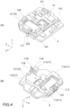
- (A) of Fig. 4 is a bottom perspective view illustrating a state in which the spacer component 1 is assembled to the front board 2, and (B) of Fig. 4 is a top perspective view illustrating a state in which the spacer component 1 is assembled to the rear board 3.
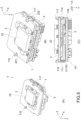
- (A) of Fig. 5 is a top perspective view illustrating a state in which the spacer component 1 is assembled to the front board 2 and the rear board 3
- (B) of Fig. 5 is a cross-sectional perspective view illustrating the state of (A)
- (C) of Fig. 5 is a cross-sectional side view illustrating the state of (A).
- the spacer component 1 is generally rectangular in appearance.
- the size of the spacer component 1 is not particularly limited, and is typically formed to be sized nearly equally to the front board 2 and the rear board 3.
- the surface 11 of the spacer component 1 is formed of a plurality of reference surfaces (first reference surfaces). As illustrated in Fig. 3 and (B) of Fig. 4 , the plurality of reference surfaces includes four reference surfaces 111, 112, 113, and 114.
- the reference surfaces 111 to 114 of the plurality of reference surfaces are planar portions that are in plane with each other (belong to the front surface 11), and are brought into contact with the back surface of the front board 2 when the spacer component 1 and the front board 2 are arranged in a layered formation (refer to (C) of Fig. 5 ).
- reference surfaces 111 to 114 of the plurality of reference surfaces may be in different planes without being in plane with each other.
- Locations at which the reference surfaces 111 to 114 are formed are not particularly limited, and can be set as appropriate according to the locations and the sizes of the components mounted on the back surface of the front board 2.
- the reference surfaces 111 to 114 are typically formed in a peripheral edge of the front surface 11 of the spacer component 1 to support a region, on the back surface of the front board 2, on which no component is mounted. In the present embodiment, the reference surfaces 111 to 114 are respectively formed at four corners of the front surface 11 of the spacer component 1.
- Shapes and sizes of the reference surfaces 111 to 114 are not particularly limited, and the reference surfaces 111 to 114 are typically formed to have different shapes and different sizes.
- the reference surfaces 111 and 113 are each formed into a rectangular island, the reference surface 112 is linearly formed, and the reference surface 114 is formed to have a shape that includes a bent portion.
- the front surface 11 of the spacer component 1 is not limited to being formed of the four reference surfaces 111 to 114 described above, and may be formed of at least three reference surfaces. This makes it possible to stably support the front board 2.
- Each of the reference surfaces 111 to 114 is formed by a recess of any depth being provided to any region of the front surface 11 of the spacer component 1.
- two recesses 161 and 162 are primarily formed. Regions in which the recesses 161 and 162 are formed correspond to thin portions of the spacer component 1.
- the recess 161 is formed to be deeper than the recess 162.
- the recess 161 is formed to connect the reference surface 111, the reference surface 112, and the reference surface 114.
- the recess 162 is formed to connect the reference surface 112, the reference surface 113, and the reference surface 114.
- the spacer component 1 includes a component accommodation portion 130 (a first component-accommodation portion) that accommodates therein the first connector component 23 and the second connector component 31 described above (refer to Fig. 2 ).
- the component accommodation portion 130 is a generally rectangular through-hole that passes through the recess 162.
- the component accommodation portion 130 corresponds to the component accommodation portion 115 in Fig. 2 .
- the spacer component 1 includes a component accommodation portion 133 that can accommodate therein an electronic component other than the first connector component 23 and the second connector component 31.
- the component accommodation portion 133 is a generally rectangular through-hole that passes through the recess 161.
- the spacer component 1 includes a missing portion 136 obtained by removing a portion from the recess 161.
- the missing portion 136 is provided between the reference surface 111 and the reference surface 114.
- the recesses 161 and 162 and the missing portion 136 serve as escape portions used to prevent interference between the spacer component 1 and a group of the components mounted on the back surface of the front board 2. (refer to (A) of Fig. 4 ).
- the component accommodation portion 133 serves as an escape portion used to prevent interference between the spacer component 1 and the electronic components mounted on the front surface of the rear board 3 (refer to (B) of Fig. 4 ).
- a plurality of engagement protrusions 116 and 117 used to control misalignment between the spacer component 1 and the front board 2 is provided to the front surface 11 of the spacer component 1.
- the engagement protrusion 116 includes a stem portion 116a and a claw portion 116b, the stem portion 116a being provided to a side edge 126 that is one of two side edges of the primary surface 11 of the spacer component 1, the claw portion 116b being provided to a tip of the stem portion 116a.
- the engagement protrusion 117 includes a stem portion 117a and a claw portion 117b, the stem portion 117a being provided to a side edge 127 that is another of the two side edges of the primary surface 11 of the spacer component 1, the claw portion 117b being provided to a tip of the stem portion 117a, the side edge 126 and the side edge 127 facing each other in the X direction.
- the stem portions 116a and 117a may be provided to face each other in the X direction, or may be provided to be offset from each other in the Z direction, as illustrated in Fig. 3 .
- the claw portions 116b and 117b are respectively formed to protrude from the respective tips of the stem portions 116a and 116b in parallel with the X direction, such that the claw portions 116b and 117b can be engaged with the front surface of the front board 2.
- Configurations of the claw portions 116b and 117b are not particularly limited, and it is sufficient if the claw portions 116b and 117b are formed such that the spacer component 1 can be arranged in snap-fit connection with the front board 2.
- the number of the engagement protrusions is not limited to two, and may be three or more.
- Concave portions 201 and 202 into which the stem portions 116a and 117a of the engagement protrusions 116 and 117 are respectively inserted, are respectively provided to side edges of the front board 2 that face each other (refer to (A) of Fig. 4 and (B) of Fig. 5 ).
- the concave portions 201 and 202 respectively have opening widths that are respectively sized nearly equally to stem diameters of the stem portions 116a and 117a, and control misalignment of the front board 2 with respect to the spacer component 1 in an XZ in-plane direction by the stem portions 116a and 117a respectively being inserted into the concave portions 201 and 202.
- Reception portions 118 and 119 are formed near the stem portion 116a of the engagement protrusion 116, and reception portions 120 and 121 are formed near the stem portion 117a of the engagement protrusion 117 (refer to Fig. 3 and (B) of Fig. 4 ).
- the reception portions 118 to 121 are in plane with the reference surfaces 111 to 114, and support the back surface of the front board 2 together with the reference surfaces 111 to 114 when the engagement protrusions 116 and 117 are engaged with the front board 2.
- a plurality of reference surfaces is provided on the back surface 14 of the spacer component 1.
- the plurality of reference surfaces includes four reference surfaces 141, 142, 143, and 144.
- the reference surfaces 141 to 144 of the plurality of reference surfaces are planar portions that are in plane with each other, and are brought into contact with the front surface of the rear board 3 when the spacer component 1 and the rear board 3 are arranged in a layered formation (refer to (C) of Fig. 5 ).
- reference surfaces 141 to 144 of the plurality of reference surfaces may be in different planes without being in plane with each other.
- Reference surfaces 141 to 144 are not particularly limited, and can be set as appropriate according to the locations and the sizes of the components mounted on the front surface of the rear board 3.
- the reference surfaces 141 to 144 are typically formed in a peripheral edge of the back surface 12 of the spacer component 1 to support a region, on the front surface of the rear board 3, on which no component is mounted. In the present embodiment, the reference surfaces 141 to 144 are respectively formed at four corners of the back surface 14 of the spacer component 1.
- Shapes and sizes of the reference surfaces 141 to 144 are not particularly limited, and, in the present embodiment, the reference surfaces 141 to 144 are each formed of a seat surface portion in the form of a circular plate, the seat surface portion protruding from the back surface 14 by a specified height in the Y direction.
- the number of the reference surfaces 141 to 144 is not limited to four, and it is sufficient if there are at least three reference surfaces. This makes it possible to stably support the rear board 3.
- the degree of parallelism of the front board 2 and the rear board 3 can be improved and maintained by assembling the spacer component 1 described above to the front board 2 and the rear board 3 (described later) .
- the number of components can be reduced by reducing, to one (the spacer component 1), the number of components used to control a distance between the front board 2 and the rear board 3 (a reduction in the number of factors of variations in component and assembly). Heights of components can be controlled as a whole by forming the spacer blocks between the boards 2 and 3 into one component. This makes it possible to contribute toward controlling inclination of the boards 2 and 3 with respect to each other, and to make the components themselves larger in size. This results in facilitating an assembly operation.
- the contact area of a portion used to receive the front board 2 and the rear board 3 can be made larger by designing the spacer component 1 according to a layout of the front board 2 and the rear board 3. This makes it possible to prevent the boards 2 and 3 from being inclined with respect to each other. This results in reducing, upon performing an operation of B-to-B connection, load imposed on a connector. This also results in reducing damage due to oscillation generated by the camera module 100 after a connector is mounted.
- the addition of the engagement protrusions 116 and 117 each having a snap-fit shape results in there being no need to perform an operation of fixing the spacer component 1 to the front board 2 using, for example, an adhesive or a sticky paper, and thus to perform handling more easily.
- the stem portions 116a and 116b of the engagement protrusions 116 and 117 that are respectively assembled into the concave portions 201 and 202 of the front board 2 serve as guides upon assembling, and this makes it easier to perform handling upon making B-to-B connection between the boards 2 and 3 (facilitating an assembly operation).
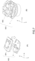
- FIGS. 6 to 8 are perspective views illustrating respective steps and being used to describe a method for producing the camera module 100.
- the spacer component 1 is assembled to the front board 2, and thus the front board 2 is placed on the primary surface 11 (the reference surfaces 111 to 114) of the spacer component 1.
- the stem portions of the engagement protrusions 116 and 117 of the spacer component 1 are respectively inserted into the concave portions 201 and 202 of the front board 2 in the Y-axis direction to be respectively assembled to the concave portions 201 and 202 (snap-fit connection).
- the claw portions 116b and 117b of the engagement protrusions 116 and 117 are engaged with a surface of the front board 2 that is opposite to a surface of the front board 2 that faces the spacer component 1, and thus the spacer component 1 and the front board 2 are integrated with each other. This results in preventing the front board 2 from falling off the spacer component 1 even when the spacer component 1 is turned upside down, and thus in performing handling more easily (facilitating an assembly operation).
- the spacer component 1 is turned upside down, and a multilayer body 501 of the spacer component 1 and the front board 2 is assembled to the rear board 2. Consequently, the rear board 3 is placed on the back surface 14 (the reference surfaces 141 to 144) of the spacer component 1, and the front board 2 and the rear board 3 are electrically and mechanically connected to each other through the first connector component 23 and the second connector component 31.
- a multilayer body 502 (the board unit 5) of the spacer component 1, the front board 2, and the rear board 3 is assembled to the lens assembly 7 through the shield case 8 and the dustproof sheet 9 (an obtained body is referred to as a multilayer body 503).
- the multilayer body 503 is assembled to the rear case 13 through the heat dissipating sheet 18 and the spacer cushion 19.
- a combining body 504 obtained by combining the multilayer body 503 and the rear case 13 is assembled to the front case 10 through the O-ring 6, and thus the camera module 100 is produced.
- the rear case 13 and the front case 10 are integrated with each other by ultrasonic welding to form a casing that integrally accommodates therein various components such as the board unit 5.
- the board unit 5 is sandwiched between the front case 10 and the rear case 13 due to an elastic force of the spacer cushion 19.
- the front board 2 is supported by the plurality of reference surfaces 111 to 114 of the front surface 11 of the spacer component 1
- the rear board 3 is supported by the plurality of reference surfaces 141 to 144 of the back surface 14 of the spacer component 1.
- the material of the spacer component may be partially changed to cause the spacer component to include an additional function as indicated below.
- Figs. 9 to 11 are schematic cross-sectional side views of spacer components of the other embodiments.
- the front board 2 and the rear board 3 are assembled to each spacer component. Note that the embodiments of Figs. 9 to 11 may be combined with each other.
- Fig. 9 illustrates a board unit 5A that includes a spacer component 1A.
- the spacer component 1A includes a component body 110 and a covering layer 151.
- the component body 110 includes, on its back surface 14, a component accommodation portion 134 with a bottom (a second component-accommodation portion).
- the covering layer 154 covers the component accommodation portion 134 to form an inner surface of the component accommodation portion 134.
- the covering layer 151 is made of an insulating material (a second insulating material) that is different from the material (the first insulating material) of the component body 110.
- the covering layer 151 is made of an electromagnetic absorbent insulating material.
- examples of such a material include a composite material such as a synthetic resin or elastomer that includes an electromagnetic absorbent material such as soft magnetic particles. This makes it possible to prevent electromagnetic waves radiated from an electronic component 32 accommodated in the component accommodation portion 134 from leaking out of the component accommodation portion 134.
- a method for forming the covering layer 151 is not particularly limited, and, in the present embodiment, the covering layer 151 is molded integrally with the component body 110 by double molding. Moreover, the covering layer 151 molded in advance may be joined to the inner surface of the component accommodation portion 134.
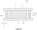
- Fig. 10 illustrates a board unit 5B that includes a spacer component 1B.
- the spacer component 1B includes the component body 110 and an interlayer connection portion 152.
- the interlayer connection portion 152 passes through the component body 110 in thickness direction of the component body 110, and makes an electrical connection between the front board 2 supported on the front surface 11 of the component body 110, and the rear board 3 supported on the back surface 14 of the component body 110.
- the interlayer connection portion 152 is formed using a conductive plastic material that includes a metal material or metal particles, and is molded integrally with the component body 110 by, for example, insert molding or double molding.
- the interlayer connection portion 152 may be configured as a portion of wiring of the front board 2 and the rear board 3, and is, for example, configured as a ground line of the board unit 5.
- Fig. 11 illustrates a board unit 5C that includes a spacer component 1C.
- the spacer component 1C includes the component body 110 and a covering layer 153.
- the component body 110 includes, on its back surface 14, a component accommodation portion 138 with a bottom (the second component-accommodation portion).
- the covering layer 154 covers the component accommodation portion 138 to form an inner surface of the component accommodation portion 138.
- the covering layer 153 is made of an insulating material (the second insulating material) that is different from the material (the first insulating material) of the component body 110.
- the covering layer 153 is made of an insulating material that is more highly thermally conductive than the component body 110. Examples of such a material include a composite material such as a synthetic resin or elastomer that includes a metallic filler. This results in obtaining an electronic component 33 having more excellent heat dissipation properties, the electronic component 33 being accommodated in the component accommodation portion 138 and generating a relatively large amount of heat.
- a method for forming the covering layer 153 is not particularly limited, and, in the present embodiment, the covering layer 153 is molded integrally with the component body 110 by double molding. Moreover, the covering layer 151 molded in advance may be joined to the inner surface of the component accommodation portion 134.
- the technology according to the present disclosure can be applied to various products.
- the technology according to the present disclosure may be provided as a camera module that is included in one of the types of mobile bodies such as vehicle, electric vehicle, hybrid electric vehicle, motorcycle, bicycle, personal mobility, airplane, drone, ship, robot, construction machinery, and agricultural machinery (a tractor).
Landscapes
- Engineering & Computer Science (AREA)
- Multimedia (AREA)
- Signal Processing (AREA)
- Microelectronics & Electronic Packaging (AREA)
- Physics & Mathematics (AREA)
- General Physics & Mathematics (AREA)
- Manufacturing & Machinery (AREA)
- Electromagnetism (AREA)
- Camera Bodies And Camera Details Or Accessories (AREA)
- Studio Devices (AREA)
Claims (12)
- Kameramodul, umfassend:eine erste Komponentenmontageplatte (2), die eine Bildgebungsvorrichtung einschließt;eine zweite Komponentenmontageplatte (3), die elektrisch mit der ersten Komponentenmontageplatte verbunden ist; undeine Abstandshalterkomponente (1), die zwischen der ersten Komponentenmontageplatte (2) und der zweiten Komponentenmontageplatte (3) angeordnet ist, wobei die Abstandshalterkomponente (1) eine einzelne Schicht eines Komponentenkörpers (110) in Form einer Platte ist oder so konfiguriert ist, dass sie einen Komponentenkörper und eine Schicht umfasst, die integral mit dem Komponentenkörper ausgebildet ist und aus einem Material einer Art besteht, die sich von der Art des Materials des Komponentenkörpers unterscheidet,wobei die Abstandshalterkomponente (1) den Komponentenkörper (110) einschließt, der aus einem ersten Isoliermaterial hergestellt ist, wobei der Komponentenkörper einen ersten Primäroberflächenabschnitt (11) mit einer Vielzahl von ersten Referenzflächen (111-114), darunter mindestens drei erste Referenzflächen, einen zweiten Primäroberflächenabschnitt (14) mit einer Vielzahl von zweiten Referenzflächen (141-144), darunter mindestens drei zweite Referenzflächen, und einen Komponentenaufnahmeabschnitt (115, 130) mit oder ohne Boden einschließt, der als Fluchtabschnitt dient, um eine gegenseitige Beeinflussung zwischen der Abstandshalterkomponente (1) und elektronischen Komponenten zu verhindern, die auf der Vorderseite der zweiten Komponentenmontageplatte (3) montiert sind, wobei der erste Primäroberflächenabschnitt (11) mit der ersten Komponentenmontageplatte (2) in Kontakt gebracht wird, der zweite Primäroberflächenabschnitt (14) mit der zweiten Komponentenmontageplatte (3) in Kontakt gebracht wird, wobei der Komponentenaufnahmeabschnitt (115, 130, 133) an mindestens einem der ersten Primäroberflächenabschnitte oder der zweiten Primäroberflächenabschnitt bereitgestellt ist;wobei die ersten Referenzflächen (111-114) als ebene Abschnitte mit unterschiedlichen Formen und unterschiedlichen Größen ausgebildet sind und die zweiten Referenzflächen (141-144) als ebene Abschnitte ausgebildet sind;wobei der Komponentenkörper (110) ferner eine Vielzahl von Eingriffsvorsprüngen (116, 117) einschließt, die eine Fehlausrichtung zwischen der Abstandskomponente (1) und der ersten Komponentenmontageplatte (2) kontrollieren, undwobei jede der Vielzahl von Eingriffsvorsprüngen (116, 117) Folgendes einschließt:einen Stammabschnitt (116a, 117a), der an einer entsprechenden der beiden Seitenkanten des ersten Primäroberflächenabschnitts bereitgestellt ist, wobei die beiden Seitenkanten einander zugewandt sind, undeinen Klauenabschnitt (116b, 117b), der an einer Spitze des Stammabschnitts bereitgestellt ist, wobei der Klauenabschnitt mit einer Oberfläche der ersten Komponentenmontageplatte in Eingriff steht, die einer Oberfläche der ersten Komponentenmontageplatte gegenüberliegt, die der Abstandshalterkomponente zugewandt ist.
- Kameramodul nach Anspruch 1, wobei
die Vielzahl der ersten Referenzflächen und die Vielzahl der zweiten Referenzflächen jeweils an einer Umfangskante des ersten Primäroberflächenabschnitts und einer Umfangskante des zweiten Primäroberflächenabschnitts bereitgestellt sind. - Kameramodul nach Anspruch 1, wobeider Komponentenaufnahmeabschnitt einen ersten Komponentenaufnahmeabschnitt umfasst, der ein Durchgangsloch ist,die erste Komponentenmontageplatte ferner eine erste Verbindungskomponente einschließt, die im Komponentenaufnahmeabschnitt untergebracht ist, unddie zweite Komponentenmontageplatte eine zweite Verbindungskomponente einschließt, die im Komponentenaufnahmeabschnitt untergebracht und mit der ersten Verbindungskomponente verbunden ist.
- Kameramodul nach Anspruch 1, wobei
die erste Komponentenmontageplatte einen konkaven Abschnitt einschließt, der an einer entsprechenden der beiden Seitenkanten der ersten Komponentenmontageplatte bereitgestellt ist, wobei der Stammabschnitt in den konkaven Abschnitt eingesetzt ist. - Kameramodul nach Anspruch 1, wobeider Komponentenaufnahmeabschnitt ferner einen zweiten Komponentenaufnahmeabschnitt mit einem Boden einschließt, unddie Abstandshalterkomponente ferner eine Deckschicht einschließt, die aus einem zweiten Isoliermaterial besteht, das sich vom ersten Isoliermaterial unterscheidet, wobei die Deckschicht eine Innenoberfläche des zweiten Komponentenaufnahmeabschnitts bildet.
- Kameramodul nach Anspruch 5, wobei
das zweite Isoliermaterial ein Verbundmaterial ist, das ein elektromagnetisches Absorptionsmaterial einschließt. - Kameramodul nach Anspruch 6, wobei
der zweite Komponentenaufnahmeabschnitt an einem Abschnitt bereitgestellt ist, der in einer Dickenrichtung der Abstandskomponente der Bildgebungsvorrichtung zugewandt ist. - Kameramodul nach Anspruch 5, wobei
das zweite Isoliermaterial eine höhere Wärmeleitfähigkeit als das erste Isoliermaterial aufweist. - Kameramodul nach Anspruch 1, wobei
die Abstandshalterkomponente ferner einen Zwischenschichtverbindungsabschnitt einschließt, der innerhalb des Komponentenkörpers bereitgestellt ist, wobei der Zwischenschichtverbindungsabschnitt eine elektrische Verbindung zwischen der ersten Komponentenmontageplatte und der zweiten Komponentenmontageplatte herstellt. - Kameramodul nach Anspruch 1, ferner umfassend:
ein Gehäuse, das einen Mehrschichtkörper aus der ersten Komponentenmontageplatte, der Abstandskomponente und der zweiten Komponentenmontageplatte integral darin aufnimmt. - Abstandshalterkomponente, umfassendeinen Komponentenkörper (110), der aus einem Isoliermaterial hergestellt ist, wobei der Komponentenkörper (110) einen ersten Primäroberflächenabschnitt (11), der eine Vielzahl von ersten Referenzflächen (111-114) einschließt, einen zweiten Primäroberflächenabschnitt (14), der eine Vielzahl von zweiten Referenzflächen (141-144) einschließt, und einen Komponentenaufnahmeabschnitt (115, 130) mit oder ohne Boden einschließt, der als ein Fluchtabschnitt dient, wobei der erste Primäroberflächenabschnitt (11) in Kontakt mit einer ersten Komponentenmontageplatte (2) gebracht wird, der zweite Primäroberflächenabschnitt (14) in Kontakt mit einer zweiten Komponentenmontageplatte (3) gebracht wird, und der Komponentenaufnahmeabschnitt (115, 130) an mindestens einem von dem ersten Primäroberflächenabschnitt (11) und dem zweiten Primäroberflächenabschnitt (14) bereitgestellt ist;wobei die ersten Referenzflächen (111-114) als ebene Abschnitte mit unterschiedlichen Formen und unterschiedlichen Größen ausgebildet sind und die zweiten Referenzflächen (141-144) als ebene Abschnitte ausgebildet sind;wobei der Komponentenkörper (110) ferner eine Vielzahl von Eingriffsvorsprüngen (116, 117) einschließt, die eine Fehlausrichtung zwischen der Abstandskomponente (1) und der ersten Komponentenmontageplatte (2) kontrollieren, undwobei jede der Vielzahl von Eingriffsvorsprüngen (116, 117) Folgendes einschließt:einen Stammabschnitt (116a, 117a), der an einer entsprechenden der beiden Seitenkanten des ersten Primäroberflächenabschnitts bereitgestellt ist, wobei die beiden Seitenkanten einander zugewandt sind, undeinen Klauenabschnitt (116b, 117b), der an einer Spitze des Stammabschnitts bereitgestellt ist, wobei der Klauenabschnitt mit einer Oberfläche der ersten Komponentenmontageplatte in Eingriff steht, die einer Oberfläche der ersten Komponentenmontageplatte gegenüberliegt, die der Abstandshalterkomponente zugewandt ist.
- Verfahren zum Herstellen eines Kameramoduls nach Anspruch 1, umfassend:Bereitstellen der Abstandshalterkomponente, die als einzelne Schicht eines Komponentenkörpers in Form einer Platte konfiguriert ist oder so konfiguriert ist, dass sie einen Komponentenkörper und eine Schicht einschließt, die integral mit dem Komponentenkörper ausgebildet ist und aus einem Materialtyp hergestellt ist, der sich vom Materialtyp des Komponentenkörpers unterscheidet und aus einem Isoliermaterial hergestellt ist, wobei die Abstandshalterkomponente einen ersten Primäroberflächenabschnitt mit einer Vielzahl von ersten Referenzflächen, einen zweiten Primäroberflächenabschnitt mit einer Vielzahl von zweiten Referenzflächen und einen Komponentenaufnahmeabschnitt ohne Boden einschließt, der als Fluchtabschnitt dient, wobei der erste Primäroberflächenabschnitt mit der ersten Komponentenmontageplatte in Kontakt gebracht wird, die eine Bildgebungsvorrichtung einschließt, und der zweite Primäroberflächenabschnitt mit der zweiten Komponentenmontageplatte in Kontakt gebracht wird, wobei der Komponentenaufnahmeabschnitt an mindestens einem von dem ersten Primäroberflächenabschnitt und dem zweiten Primäroberflächenabschnitt bereitgestellt ist,wobei die ersten Referenzflächen als ebene Abschnitte mit unterschiedlichen Formen und unterschiedlichen Größen ausgebildet sind und die zweiten Referenzflächen als ebene Abschnitte ausgebildet sind;Anordnen der ersten Komponentenmontageplatte in Schnappverbindung mit der Abstandskomponente;Platzieren der ersten Komponentenmontageplatte auf der Vielzahl von ersten Referenzflächen, um zu bewirken, dass eine erste Verbindungskomponente in dem Komponentenaufnahmeabschnitt aufgenommen wird, wobei die erste Verbindungskomponente auf der ersten Komponentenmontageplatte montiert wird;Drehen des Abstandselements auf den Kopf; undPlatzieren der zweiten Komponentenmontageplatte auf der Vielzahl von zweiten Referenzflächen, um eine zweite Verbindungskomponente mit der ersten Verbindungskomponente im Komponentenaufnahmeabschnitt zu verbinden, wobei die zweite Verbindungskomponente auf der zweiten Komponentenmontageplatte montiert wird.
Applications Claiming Priority (2)
| Application Number | Priority Date | Filing Date | Title |
|---|---|---|---|
| JP2019230753 | 2019-12-20 | ||
| PCT/JP2020/046217 WO2021125074A1 (ja) | 2019-12-20 | 2020-12-11 | カメラモジュール、スペーサ部品およびカメラモジュールの製造方法 |
Publications (3)
| Publication Number | Publication Date |
|---|---|
| EP4080263A1 EP4080263A1 (de) | 2022-10-26 |
| EP4080263A4 EP4080263A4 (de) | 2023-05-31 |
| EP4080263B1 true EP4080263B1 (de) | 2025-06-11 |
Family
ID=76478759
Family Applications (1)
| Application Number | Title | Priority Date | Filing Date |
|---|---|---|---|
| EP20901447.1A Active EP4080263B1 (de) | 2019-12-20 | 2020-12-11 | Kameramodul, abstandskomponente und verfahren zur herstellung eines kameramoduls |
Country Status (6)
| Country | Link |
|---|---|
| US (1) | US11930258B2 (de) |
| EP (1) | EP4080263B1 (de) |
| JP (1) | JP7707079B2 (de) |
| KR (1) | KR102896429B1 (de) |
| CN (1) | CN114787680B (de) |
| WO (1) | WO2021125074A1 (de) |
Families Citing this family (6)
| Publication number | Priority date | Publication date | Assignee | Title |
|---|---|---|---|---|
| JP6780689B2 (ja) * | 2018-11-21 | 2020-11-04 | I−Pex株式会社 | 電気コネクタ及びコネクタ装置 |
| JPWO2023135720A1 (de) * | 2022-01-14 | 2023-07-20 | ||
| WO2024004821A1 (ja) | 2022-06-29 | 2024-01-04 | パナソニックIpマネジメント株式会社 | 車載用カメラ |
| EP4357848B1 (de) * | 2022-10-21 | 2026-01-07 | Aptiv Technologies AG | Kamera und verfahren zur herstellung einer kamera |
| JP2025018344A (ja) * | 2023-07-26 | 2025-02-06 | パナソニックオートモーティブシステムズ株式会社 | 車載用カメラ |
| US12610114B2 (en) * | 2023-08-07 | 2026-04-21 | Panasonic Automotive Systems Co., Ltd. | Vehicular camera |
Family Cites Families (25)
| Publication number | Priority date | Publication date | Assignee | Title |
|---|---|---|---|---|
| JP2000241864A (ja) | 1999-02-24 | 2000-09-08 | Canon Inc | 光学センサー取り付け装置およびカメラ |
| JP3927074B2 (ja) | 2002-05-27 | 2007-06-06 | オリンパス株式会社 | カメラ及びこれに用いる撮像素子ユニット |
| US7324148B2 (en) | 2002-04-26 | 2008-01-29 | Olympus Optical Co., Ltd. | Camera and image pickup device unit used therefor having a sealing structure between a dust proofing member and an image pick up device |
| JP4012428B2 (ja) * | 2002-04-30 | 2007-11-21 | 富士フイルム株式会社 | 撮像素子ユニット |
| CA2584720A1 (en) * | 2004-10-26 | 2006-05-04 | Richco Inc. | Spring loaded spacer |
| WO2008133943A1 (en) * | 2007-04-24 | 2008-11-06 | Flextronics Ap Llc | Small form factor modules using wafer level optics with bottom cavity and flip chip assembly |
| JP5321954B2 (ja) * | 2008-08-28 | 2013-10-23 | コニカミノルタ株式会社 | 撮像レンズ、撮像装置及び携帯端末 |
| KR101563484B1 (ko) * | 2009-01-06 | 2015-10-27 | 삼성전자 주식회사 | 스위치 조립체 및 이를 포함하는 공기조화기 |
| TWI374694B (en) * | 2009-07-23 | 2012-10-11 | Acbel Polytech Inc | Circuit board module and power supply |
| US9079546B2 (en) | 2010-12-14 | 2015-07-14 | Mitsubishi Electric Corporation | Vehicle-mounted information apparatus |
| JP5971942B2 (ja) | 2011-12-27 | 2016-08-17 | キヤノン株式会社 | 電子機器 |
| JP2013179564A (ja) | 2012-02-01 | 2013-09-09 | Canon Inc | 画像処理方法、画像処理装置および撮像装置 |
| JP2013172245A (ja) * | 2012-02-20 | 2013-09-02 | Sony Corp | カメラ装置、電子装置およびフレキシブルシャーシ |
| TWI627761B (zh) * | 2012-07-17 | 2018-06-21 | 新加坡恒立私人有限公司 | 用以感測一量度的感測器模組,其應用器具,其製造方法,裝置的製造方法,及包含光譜計模組的裝置 |
| JP2014153690A (ja) | 2013-02-14 | 2014-08-25 | Alps Electric Co Ltd | レンズ駆動装置 |
| JP6453158B2 (ja) * | 2015-05-25 | 2019-01-16 | 株式会社オプトエレクトロニクス | 撮像装置及び光学的情報読取装置 |
| KR102406627B1 (ko) * | 2015-10-21 | 2022-06-08 | 엘지이노텍 주식회사 | 카메라 모듈 |
| CN113382150B (zh) * | 2015-10-30 | 2023-05-19 | 佳能株式会社 | 电子装置和照相机模块 |
| JP6624939B2 (ja) | 2016-01-14 | 2019-12-25 | キヤノン株式会社 | 画像処理装置、撮像装置および画像処理プログラム |
| JP6939568B2 (ja) * | 2016-01-15 | 2021-09-22 | ソニーグループ株式会社 | 半導体装置および撮像装置 |
| WO2017142978A1 (en) * | 2016-02-15 | 2017-08-24 | Transsip Inc | Emi shielded integrated circuit packages and methods of making the same |
| CN107455005B (zh) | 2016-09-27 | 2020-05-05 | 深圳市大疆创新科技有限公司 | 相机及拍摄组件 |
| KR102612541B1 (ko) | 2016-10-18 | 2023-12-12 | 엘지이노텍 주식회사 | 카메라 모듈 |
| JP7146376B2 (ja) * | 2017-08-31 | 2022-10-04 | ソニーセミコンダクタソリューションズ株式会社 | 撮像装置、および電子機器 |
| TWI672083B (zh) * | 2017-10-19 | 2019-09-11 | 啓碁科技股份有限公司 | 影像擷取裝置 |
-
2020
- 2020-12-11 WO PCT/JP2020/046217 patent/WO2021125074A1/ja not_active Ceased
- 2020-12-11 CN CN202080086189.4A patent/CN114787680B/zh active Active
- 2020-12-11 KR KR1020227018849A patent/KR102896429B1/ko active Active
- 2020-12-11 EP EP20901447.1A patent/EP4080263B1/de active Active
- 2020-12-11 JP JP2021565544A patent/JP7707079B2/ja active Active
- 2020-12-11 US US17/785,013 patent/US11930258B2/en active Active
Also Published As
| Publication number | Publication date |
|---|---|
| EP4080263A1 (de) | 2022-10-26 |
| CN114787680A (zh) | 2022-07-22 |
| EP4080263A4 (de) | 2023-05-31 |
| JPWO2021125074A1 (de) | 2021-06-24 |
| WO2021125074A1 (ja) | 2021-06-24 |
| JP7707079B2 (ja) | 2025-07-14 |
| CN114787680B (zh) | 2026-01-23 |
| US20230008374A1 (en) | 2023-01-12 |
| KR20220116161A (ko) | 2022-08-22 |
| US11930258B2 (en) | 2024-03-12 |
| KR102896429B1 (ko) | 2025-12-08 |
Similar Documents
| Publication | Publication Date | Title |
|---|---|---|
| EP4080263B1 (de) | Kameramodul, abstandskomponente und verfahren zur herstellung eines kameramoduls | |
| KR102213027B1 (ko) | 차폐된 이미저 회로를 구비한 카메라 어셈블리 | |
| CN105409056B (zh) | 紧凑型屏蔽的车载雷达模块和方法 | |
| US9345134B2 (en) | Printed wiring board | |
| US9160908B2 (en) | Imaging apparatus | |
| CN207968641U (zh) | 摄像头模块 | |
| CZ232198A3 (cs) | Řídící přístroj, zejména pro motorové vozidlo | |
| GB2413435A (en) | Camera lens module and method of assembly thereof | |
| US9215360B2 (en) | Camera module having shield can | |
| US7645981B2 (en) | Image pickup device mounting structure for saving space in an optical device | |
| US10582631B2 (en) | Housings formed from three-dimensional circuits | |
| US20110157462A1 (en) | Camera module | |
| JP5733456B1 (ja) | 基板接続用コネクタ | |
| JP5564844B2 (ja) | 電子装置 | |
| US9491848B2 (en) | Grounding part, electronic device, imaging device, and grounding part production method | |
| US10313571B2 (en) | Imager module for vehicle | |
| JP2013029614A (ja) | 撮像装置 | |
| CN108781526A (zh) | 电子设备 | |
| CN113632446B (zh) | 电子设备、拍摄装置以及移动体 | |
| CN114498145A (zh) | 连接器 | |
| US20150062424A1 (en) | Camera module and method for assembling same | |
| JP2026037049A (ja) | ソケット及びソケットの製造方法 | |
| JP6628608B2 (ja) | 電子機器及び撮像装置 | |
| CN205140982U (zh) | 多层基板与光接收模块 | |
| WO2022113743A1 (ja) | 接続部品、シールドモジュール、及び電子機器 |
Legal Events
| Date | Code | Title | Description |
|---|---|---|---|
| STAA | Information on the status of an ep patent application or granted ep patent |
Free format text: STATUS: THE INTERNATIONAL PUBLICATION HAS BEEN MADE |
|
| PUAI | Public reference made under article 153(3) epc to a published international application that has entered the european phase |
Free format text: ORIGINAL CODE: 0009012 |
|
| STAA | Information on the status of an ep patent application or granted ep patent |
Free format text: STATUS: REQUEST FOR EXAMINATION WAS MADE |
|
| 17P | Request for examination filed |
Effective date: 20220608 |
|
| AK | Designated contracting states |
Kind code of ref document: A1 Designated state(s): AL AT BE BG CH CY CZ DE DK EE ES FI FR GB GR HR HU IE IS IT LI LT LU LV MC MK MT NL NO PL PT RO RS SE SI SK SM TR |
|
| A4 | Supplementary search report drawn up and despatched |
Effective date: 20230502 |
|
| RIC1 | Information provided on ipc code assigned before grant |
Ipc: H05K 3/36 20060101ALI20230424BHEP Ipc: H05K 1/18 20060101ALI20230424BHEP Ipc: H05K 1/14 20060101ALI20230424BHEP Ipc: H04N 23/57 20230101ALI20230424BHEP Ipc: H04N 23/54 20230101ALI20230424BHEP Ipc: G03B 30/00 20210101ALI20230424BHEP Ipc: G03B 17/02 20210101ALI20230424BHEP Ipc: G02B 7/02 20210101AFI20230424BHEP |
|
| REG | Reference to a national code |
Ref country code: DE Ref legal event code: R079 Free format text: PREVIOUS MAIN CLASS: G02B0007020000 Ipc: H04N0023510000 Ref country code: DE Ref legal event code: R079 Ref document number: 602020052757 Country of ref document: DE Free format text: PREVIOUS MAIN CLASS: G02B0007020000 Ipc: H04N0023510000 |
|
| GRAP | Despatch of communication of intention to grant a patent |
Free format text: ORIGINAL CODE: EPIDOSNIGR1 |
|
| STAA | Information on the status of an ep patent application or granted ep patent |
Free format text: STATUS: GRANT OF PATENT IS INTENDED |
|
| RIC1 | Information provided on ipc code assigned before grant |
Ipc: H05K 3/36 20060101ALI20241212BHEP Ipc: H05K 1/18 20060101ALI20241212BHEP Ipc: H05K 1/14 20060101ALI20241212BHEP Ipc: G03B 30/00 20210101ALI20241212BHEP Ipc: G03B 17/02 20210101ALI20241212BHEP Ipc: G02B 7/02 20210101ALI20241212BHEP Ipc: H04N 23/57 20230101ALI20241212BHEP Ipc: H04N 23/51 20230101AFI20241212BHEP |
|
| INTG | Intention to grant announced |
Effective date: 20250107 |
|
| GRAS | Grant fee paid |
Free format text: ORIGINAL CODE: EPIDOSNIGR3 |
|
| GRAA | (expected) grant |
Free format text: ORIGINAL CODE: 0009210 |
|
| STAA | Information on the status of an ep patent application or granted ep patent |
Free format text: STATUS: THE PATENT HAS BEEN GRANTED |
|
| P01 | Opt-out of the competence of the unified patent court (upc) registered |
Free format text: CASE NUMBER: APP_18555/2025 Effective date: 20250416 |
|
| AK | Designated contracting states |
Kind code of ref document: B1 Designated state(s): AL AT BE BG CH CY CZ DE DK EE ES FI FR GB GR HR HU IE IS IT LI LT LU LV MC MK MT NL NO PL PT RO RS SE SI SK SM TR |
|
| REG | Reference to a national code |
Ref country code: GB Ref legal event code: FG4D |
|
| REG | Reference to a national code |
Ref country code: CH Ref legal event code: EP |
|
| REG | Reference to a national code |
Ref country code: IE Ref legal event code: FG4D |
|
| REG | Reference to a national code |
Ref country code: DE Ref legal event code: R096 Ref document number: 602020052757 Country of ref document: DE |
|
| REG | Reference to a national code |
Ref country code: NL Ref legal event code: FP |
|
| PG25 | Lapsed in a contracting state [announced via postgrant information from national office to epo] |
Ref country code: FI Free format text: LAPSE BECAUSE OF FAILURE TO SUBMIT A TRANSLATION OF THE DESCRIPTION OR TO PAY THE FEE WITHIN THE PRESCRIBED TIME-LIMIT Effective date: 20250611 Ref country code: ES Free format text: LAPSE BECAUSE OF FAILURE TO SUBMIT A TRANSLATION OF THE DESCRIPTION OR TO PAY THE FEE WITHIN THE PRESCRIBED TIME-LIMIT Effective date: 20250611 |
|
| REG | Reference to a national code |
Ref country code: LT Ref legal event code: MG9D |
|
| PG25 | Lapsed in a contracting state [announced via postgrant information from national office to epo] |
Ref country code: NO Free format text: LAPSE BECAUSE OF FAILURE TO SUBMIT A TRANSLATION OF THE DESCRIPTION OR TO PAY THE FEE WITHIN THE PRESCRIBED TIME-LIMIT Effective date: 20250911 Ref country code: GR Free format text: LAPSE BECAUSE OF FAILURE TO SUBMIT A TRANSLATION OF THE DESCRIPTION OR TO PAY THE FEE WITHIN THE PRESCRIBED TIME-LIMIT Effective date: 20250912 |
|
| PG25 | Lapsed in a contracting state [announced via postgrant information from national office to epo] |
Ref country code: BG Free format text: LAPSE BECAUSE OF FAILURE TO SUBMIT A TRANSLATION OF THE DESCRIPTION OR TO PAY THE FEE WITHIN THE PRESCRIBED TIME-LIMIT Effective date: 20250611 |
|
| PG25 | Lapsed in a contracting state [announced via postgrant information from national office to epo] |
Ref country code: HR Free format text: LAPSE BECAUSE OF FAILURE TO SUBMIT A TRANSLATION OF THE DESCRIPTION OR TO PAY THE FEE WITHIN THE PRESCRIBED TIME-LIMIT Effective date: 20250611 |
|
| PG25 | Lapsed in a contracting state [announced via postgrant information from national office to epo] |
Ref country code: RS Free format text: LAPSE BECAUSE OF FAILURE TO SUBMIT A TRANSLATION OF THE DESCRIPTION OR TO PAY THE FEE WITHIN THE PRESCRIBED TIME-LIMIT Effective date: 20250911 |
|
| PG25 | Lapsed in a contracting state [announced via postgrant information from national office to epo] |
Ref country code: LV Free format text: LAPSE BECAUSE OF FAILURE TO SUBMIT A TRANSLATION OF THE DESCRIPTION OR TO PAY THE FEE WITHIN THE PRESCRIBED TIME-LIMIT Effective date: 20250611 |
|
| PG25 | Lapsed in a contracting state [announced via postgrant information from national office to epo] |
Ref country code: PT Free format text: LAPSE BECAUSE OF FAILURE TO SUBMIT A TRANSLATION OF THE DESCRIPTION OR TO PAY THE FEE WITHIN THE PRESCRIBED TIME-LIMIT Effective date: 20251013 |
|
| PGFP | Annual fee paid to national office [announced via postgrant information from national office to epo] |
Ref country code: NL Payment date: 20251119 Year of fee payment: 6 |
|
| REG | Reference to a national code |
Ref country code: AT Ref legal event code: MK05 Ref document number: 1803192 Country of ref document: AT Kind code of ref document: T Effective date: 20250611 |
|
| PG25 | Lapsed in a contracting state [announced via postgrant information from national office to epo] |
Ref country code: IS Free format text: LAPSE BECAUSE OF FAILURE TO SUBMIT A TRANSLATION OF THE DESCRIPTION OR TO PAY THE FEE WITHIN THE PRESCRIBED TIME-LIMIT Effective date: 20251011 |
|
| PGFP | Annual fee paid to national office [announced via postgrant information from national office to epo] |
Ref country code: DE Payment date: 20251126 Year of fee payment: 6 |
|
| PGFP | Annual fee paid to national office [announced via postgrant information from national office to epo] |
Ref country code: GB Payment date: 20251120 Year of fee payment: 6 |
|
| PG25 | Lapsed in a contracting state [announced via postgrant information from national office to epo] |
Ref country code: SM Free format text: LAPSE BECAUSE OF FAILURE TO SUBMIT A TRANSLATION OF THE DESCRIPTION OR TO PAY THE FEE WITHIN THE PRESCRIBED TIME-LIMIT Effective date: 20250611 Ref country code: AT Free format text: LAPSE BECAUSE OF FAILURE TO SUBMIT A TRANSLATION OF THE DESCRIPTION OR TO PAY THE FEE WITHIN THE PRESCRIBED TIME-LIMIT Effective date: 20250611 |
|
| PGFP | Annual fee paid to national office [announced via postgrant information from national office to epo] |
Ref country code: FR Payment date: 20251120 Year of fee payment: 6 |
|
| PG25 | Lapsed in a contracting state [announced via postgrant information from national office to epo] |
Ref country code: CZ Free format text: LAPSE BECAUSE OF FAILURE TO SUBMIT A TRANSLATION OF THE DESCRIPTION OR TO PAY THE FEE WITHIN THE PRESCRIBED TIME-LIMIT Effective date: 20250611 |
|
| PG25 | Lapsed in a contracting state [announced via postgrant information from national office to epo] |
Ref country code: PL Free format text: LAPSE BECAUSE OF FAILURE TO SUBMIT A TRANSLATION OF THE DESCRIPTION OR TO PAY THE FEE WITHIN THE PRESCRIBED TIME-LIMIT Effective date: 20250611 |
|
| PG25 | Lapsed in a contracting state [announced via postgrant information from national office to epo] |
Ref country code: EE Free format text: LAPSE BECAUSE OF FAILURE TO SUBMIT A TRANSLATION OF THE DESCRIPTION OR TO PAY THE FEE WITHIN THE PRESCRIBED TIME-LIMIT Effective date: 20250611 |
|
| PG25 | Lapsed in a contracting state [announced via postgrant information from national office to epo] |
Ref country code: SK Free format text: LAPSE BECAUSE OF FAILURE TO SUBMIT A TRANSLATION OF THE DESCRIPTION OR TO PAY THE FEE WITHIN THE PRESCRIBED TIME-LIMIT Effective date: 20250611 |
|
| PG25 | Lapsed in a contracting state [announced via postgrant information from national office to epo] |
Ref country code: RO Free format text: LAPSE BECAUSE OF FAILURE TO SUBMIT A TRANSLATION OF THE DESCRIPTION OR TO PAY THE FEE WITHIN THE PRESCRIBED TIME-LIMIT Effective date: 20250611 |
|
| REG | Reference to a national code |
Ref country code: DE Ref legal event code: R097 Ref document number: 602020052757 Country of ref document: DE |
|
| PG25 | Lapsed in a contracting state [announced via postgrant information from national office to epo] |
Ref country code: DK Free format text: LAPSE BECAUSE OF FAILURE TO SUBMIT A TRANSLATION OF THE DESCRIPTION OR TO PAY THE FEE WITHIN THE PRESCRIBED TIME-LIMIT Effective date: 20250611 |
|
| PG25 | Lapsed in a contracting state [announced via postgrant information from national office to epo] |
Ref country code: IT Free format text: LAPSE BECAUSE OF FAILURE TO SUBMIT A TRANSLATION OF THE DESCRIPTION OR TO PAY THE FEE WITHIN THE PRESCRIBED TIME-LIMIT Effective date: 20250611 |
|
| PLBE | No opposition filed within time limit |
Free format text: ORIGINAL CODE: 0009261 |
|
| STAA | Information on the status of an ep patent application or granted ep patent |
Free format text: STATUS: NO OPPOSITION FILED WITHIN TIME LIMIT |
|
| REG | Reference to a national code |
Ref country code: CH Ref legal event code: L10 Free format text: ST27 STATUS EVENT CODE: U-0-0-L10-L00 (AS PROVIDED BY THE NATIONAL OFFICE) Effective date: 20260423 |