EP4080564A1 - Contact électrique d'un élément de circuit applicable à un porte-circuit ou d'un connecteur électrique, ainsi que procédé d'établissement d'une connexion électriquement conductrice - Google Patents
Contact électrique d'un élément de circuit applicable à un porte-circuit ou d'un connecteur électrique, ainsi que procédé d'établissement d'une connexion électriquement conductrice Download PDFInfo
- Publication number
- EP4080564A1 EP4080564A1 EP21169988.9A EP21169988A EP4080564A1 EP 4080564 A1 EP4080564 A1 EP 4080564A1 EP 21169988 A EP21169988 A EP 21169988A EP 4080564 A1 EP4080564 A1 EP 4080564A1
- Authority
- EP
- European Patent Office
- Prior art keywords
- contact
- porous
- foam
- circuit
- contacts
- Prior art date
- Legal status (The legal status is an assumption and is not a legal conclusion. Google has not performed a legal analysis and makes no representation as to the accuracy of the status listed.)
- Withdrawn
Links
Images
Classifications
-
- H—ELECTRICITY
- H10—SEMICONDUCTOR DEVICES; ELECTRIC SOLID-STATE DEVICES NOT OTHERWISE PROVIDED FOR
- H10W—GENERIC PACKAGES, INTERCONNECTIONS, CONNECTORS OR OTHER CONSTRUCTIONAL DETAILS OF DEVICES COVERED BY CLASS H10
- H10W72/00—Interconnections or connectors in packages
- H10W72/071—Connecting or disconnecting
- H10W72/073—Connecting or disconnecting of die-attach connectors
-
- H—ELECTRICITY
- H10—SEMICONDUCTOR DEVICES; ELECTRIC SOLID-STATE DEVICES NOT OTHERWISE PROVIDED FOR
- H10W—GENERIC PACKAGES, INTERCONNECTIONS, CONNECTORS OR OTHER CONSTRUCTIONAL DETAILS OF DEVICES COVERED BY CLASS H10
- H10W72/00—Interconnections or connectors in packages
- H10W72/01—Manufacture or treatment
- H10W72/012—Manufacture or treatment of bump connectors, dummy bumps or thermal bumps
- H10W72/01215—Manufacture or treatment of bump connectors, dummy bumps or thermal bumps forming coatings
-
- H—ELECTRICITY
- H10—SEMICONDUCTOR DEVICES; ELECTRIC SOLID-STATE DEVICES NOT OTHERWISE PROVIDED FOR
- H10W—GENERIC PACKAGES, INTERCONNECTIONS, CONNECTORS OR OTHER CONSTRUCTIONAL DETAILS OF DEVICES COVERED BY CLASS H10
- H10W72/00—Interconnections or connectors in packages
- H10W72/01—Manufacture or treatment
- H10W72/012—Manufacture or treatment of bump connectors, dummy bumps or thermal bumps
- H10W72/01231—Manufacture or treatment of bump connectors, dummy bumps or thermal bumps using blanket deposition
- H10W72/01233—Manufacture or treatment of bump connectors, dummy bumps or thermal bumps using blanket deposition in liquid form, e.g. spin coating, spray coating or immersion coating
- H10W72/01235—Manufacture or treatment of bump connectors, dummy bumps or thermal bumps using blanket deposition in liquid form, e.g. spin coating, spray coating or immersion coating by plating, e.g. electroless plating or electroplating
-
- H—ELECTRICITY
- H10—SEMICONDUCTOR DEVICES; ELECTRIC SOLID-STATE DEVICES NOT OTHERWISE PROVIDED FOR
- H10W—GENERIC PACKAGES, INTERCONNECTIONS, CONNECTORS OR OTHER CONSTRUCTIONAL DETAILS OF DEVICES COVERED BY CLASS H10
- H10W72/00—Interconnections or connectors in packages
- H10W72/01—Manufacture or treatment
- H10W72/012—Manufacture or treatment of bump connectors, dummy bumps or thermal bumps
- H10W72/01261—Chemical or physical modification, e.g. by sintering or anodisation
-
- H—ELECTRICITY
- H10—SEMICONDUCTOR DEVICES; ELECTRIC SOLID-STATE DEVICES NOT OTHERWISE PROVIDED FOR
- H10W—GENERIC PACKAGES, INTERCONNECTIONS, CONNECTORS OR OTHER CONSTRUCTIONAL DETAILS OF DEVICES COVERED BY CLASS H10
- H10W72/00—Interconnections or connectors in packages
- H10W72/071—Connecting or disconnecting
- H10W72/072—Connecting or disconnecting of bump connectors
-
- H—ELECTRICITY
- H10—SEMICONDUCTOR DEVICES; ELECTRIC SOLID-STATE DEVICES NOT OTHERWISE PROVIDED FOR
- H10W—GENERIC PACKAGES, INTERCONNECTIONS, CONNECTORS OR OTHER CONSTRUCTIONAL DETAILS OF DEVICES COVERED BY CLASS H10
- H10W72/00—Interconnections or connectors in packages
- H10W72/071—Connecting or disconnecting
- H10W72/072—Connecting or disconnecting of bump connectors
- H10W72/07221—Aligning
- H10W72/07227—Aligning involving guiding structures, e.g. spacers or supporting members
-
- H—ELECTRICITY
- H10—SEMICONDUCTOR DEVICES; ELECTRIC SOLID-STATE DEVICES NOT OTHERWISE PROVIDED FOR
- H10W—GENERIC PACKAGES, INTERCONNECTIONS, CONNECTORS OR OTHER CONSTRUCTIONAL DETAILS OF DEVICES COVERED BY CLASS H10
- H10W72/00—Interconnections or connectors in packages
- H10W72/071—Connecting or disconnecting
- H10W72/072—Connecting or disconnecting of bump connectors
- H10W72/07231—Techniques
- H10W72/07232—Compression bonding, e.g. thermocompression bonding
-
- H—ELECTRICITY
- H10—SEMICONDUCTOR DEVICES; ELECTRIC SOLID-STATE DEVICES NOT OTHERWISE PROVIDED FOR
- H10W—GENERIC PACKAGES, INTERCONNECTIONS, CONNECTORS OR OTHER CONSTRUCTIONAL DETAILS OF DEVICES COVERED BY CLASS H10
- H10W72/00—Interconnections or connectors in packages
- H10W72/071—Connecting or disconnecting
- H10W72/072—Connecting or disconnecting of bump connectors
- H10W72/07231—Techniques
- H10W72/07232—Compression bonding, e.g. thermocompression bonding
- H10W72/07233—Ultrasonic bonding, e.g. thermosonic bonding
-
- H—ELECTRICITY
- H10—SEMICONDUCTOR DEVICES; ELECTRIC SOLID-STATE DEVICES NOT OTHERWISE PROVIDED FOR
- H10W—GENERIC PACKAGES, INTERCONNECTIONS, CONNECTORS OR OTHER CONSTRUCTIONAL DETAILS OF DEVICES COVERED BY CLASS H10
- H10W72/00—Interconnections or connectors in packages
- H10W72/071—Connecting or disconnecting
- H10W72/072—Connecting or disconnecting of bump connectors
- H10W72/07231—Techniques
- H10W72/07235—Applying EM radiation, e.g. induction heating or using a laser
-
- H—ELECTRICITY
- H10—SEMICONDUCTOR DEVICES; ELECTRIC SOLID-STATE DEVICES NOT OTHERWISE PROVIDED FOR
- H10W—GENERIC PACKAGES, INTERCONNECTIONS, CONNECTORS OR OTHER CONSTRUCTIONAL DETAILS OF DEVICES COVERED BY CLASS H10
- H10W72/00—Interconnections or connectors in packages
- H10W72/071—Connecting or disconnecting
- H10W72/073—Connecting or disconnecting of die-attach connectors
- H10W72/07321—Aligning
- H10W72/07327—Aligning involving guiding structures, e.g. spacers or supporting members
-
- H—ELECTRICITY
- H10—SEMICONDUCTOR DEVICES; ELECTRIC SOLID-STATE DEVICES NOT OTHERWISE PROVIDED FOR
- H10W—GENERIC PACKAGES, INTERCONNECTIONS, CONNECTORS OR OTHER CONSTRUCTIONAL DETAILS OF DEVICES COVERED BY CLASS H10
- H10W72/00—Interconnections or connectors in packages
- H10W72/071—Connecting or disconnecting
- H10W72/073—Connecting or disconnecting of die-attach connectors
- H10W72/07331—Connecting techniques
- H10W72/07332—Compression bonding, e.g. thermocompression bonding
- H10W72/07333—Ultrasonic bonding, e.g. thermosonic bonding
-
- H—ELECTRICITY
- H10—SEMICONDUCTOR DEVICES; ELECTRIC SOLID-STATE DEVICES NOT OTHERWISE PROVIDED FOR
- H10W—GENERIC PACKAGES, INTERCONNECTIONS, CONNECTORS OR OTHER CONSTRUCTIONAL DETAILS OF DEVICES COVERED BY CLASS H10
- H10W72/00—Interconnections or connectors in packages
- H10W72/071—Connecting or disconnecting
- H10W72/073—Connecting or disconnecting of die-attach connectors
- H10W72/07331—Connecting techniques
- H10W72/07335—Applying EM radiation, e.g. induction heating or using a laser
-
- H—ELECTRICITY
- H10—SEMICONDUCTOR DEVICES; ELECTRIC SOLID-STATE DEVICES NOT OTHERWISE PROVIDED FOR
- H10W—GENERIC PACKAGES, INTERCONNECTIONS, CONNECTORS OR OTHER CONSTRUCTIONAL DETAILS OF DEVICES COVERED BY CLASS H10
- H10W72/00—Interconnections or connectors in packages
- H10W72/071—Connecting or disconnecting
- H10W72/074—Connecting or disconnecting of anisotropic conductive adhesives
-
- H—ELECTRICITY
- H10—SEMICONDUCTOR DEVICES; ELECTRIC SOLID-STATE DEVICES NOT OTHERWISE PROVIDED FOR
- H10W—GENERIC PACKAGES, INTERCONNECTIONS, CONNECTORS OR OTHER CONSTRUCTIONAL DETAILS OF DEVICES COVERED BY CLASS H10
- H10W72/00—Interconnections or connectors in packages
- H10W72/20—Bump connectors, e.g. solder bumps or copper pillars; Dummy bumps; Thermal bumps
- H10W72/241—Dispositions, e.g. layouts
- H10W72/247—Dispositions of multiple bumps
- H10W72/248—Top-view layouts, e.g. mirror arrays
-
- H—ELECTRICITY
- H10—SEMICONDUCTOR DEVICES; ELECTRIC SOLID-STATE DEVICES NOT OTHERWISE PROVIDED FOR
- H10W—GENERIC PACKAGES, INTERCONNECTIONS, CONNECTORS OR OTHER CONSTRUCTIONAL DETAILS OF DEVICES COVERED BY CLASS H10
- H10W72/00—Interconnections or connectors in packages
- H10W72/20—Bump connectors, e.g. solder bumps or copper pillars; Dummy bumps; Thermal bumps
- H10W72/251—Materials
- H10W72/252—Materials comprising solid metals or solid metalloids, e.g. PbSn, Ag or Cu
-
- H—ELECTRICITY
- H10—SEMICONDUCTOR DEVICES; ELECTRIC SOLID-STATE DEVICES NOT OTHERWISE PROVIDED FOR
- H10W—GENERIC PACKAGES, INTERCONNECTIONS, CONNECTORS OR OTHER CONSTRUCTIONAL DETAILS OF DEVICES COVERED BY CLASS H10
- H10W72/00—Interconnections or connectors in packages
- H10W72/20—Bump connectors, e.g. solder bumps or copper pillars; Dummy bumps; Thermal bumps
- H10W72/251—Materials
- H10W72/255—Materials of outermost layers of multilayered bumps, e.g. material of a coating
-
- H—ELECTRICITY
- H10—SEMICONDUCTOR DEVICES; ELECTRIC SOLID-STATE DEVICES NOT OTHERWISE PROVIDED FOR
- H10W—GENERIC PACKAGES, INTERCONNECTIONS, CONNECTORS OR OTHER CONSTRUCTIONAL DETAILS OF DEVICES COVERED BY CLASS H10
- H10W72/00—Interconnections or connectors in packages
- H10W72/30—Die-attach connectors
- H10W72/321—Structures or relative sizes of die-attach connectors
- H10W72/325—Die-attach connectors having a filler embedded in a matrix
-
- H—ELECTRICITY
- H10—SEMICONDUCTOR DEVICES; ELECTRIC SOLID-STATE DEVICES NOT OTHERWISE PROVIDED FOR
- H10W—GENERIC PACKAGES, INTERCONNECTIONS, CONNECTORS OR OTHER CONSTRUCTIONAL DETAILS OF DEVICES COVERED BY CLASS H10
- H10W72/00—Interconnections or connectors in packages
- H10W72/30—Die-attach connectors
- H10W72/351—Materials of die-attach connectors
- H10W72/352—Materials of die-attach connectors comprising metals or metalloids, e.g. solders
-
- H—ELECTRICITY
- H10—SEMICONDUCTOR DEVICES; ELECTRIC SOLID-STATE DEVICES NOT OTHERWISE PROVIDED FOR
- H10W—GENERIC PACKAGES, INTERCONNECTIONS, CONNECTORS OR OTHER CONSTRUCTIONAL DETAILS OF DEVICES COVERED BY CLASS H10
- H10W72/00—Interconnections or connectors in packages
- H10W72/30—Die-attach connectors
- H10W72/351—Materials of die-attach connectors
- H10W72/353—Materials of die-attach connectors not comprising solid metals or solid metalloids, e.g. ceramics
-
- H—ELECTRICITY
- H10—SEMICONDUCTOR DEVICES; ELECTRIC SOLID-STATE DEVICES NOT OTHERWISE PROVIDED FOR
- H10W—GENERIC PACKAGES, INTERCONNECTIONS, CONNECTORS OR OTHER CONSTRUCTIONAL DETAILS OF DEVICES COVERED BY CLASS H10
- H10W72/00—Interconnections or connectors in packages
- H10W72/90—Bond pads, in general
- H10W72/931—Shapes of bond pads
-
- H—ELECTRICITY
- H10—SEMICONDUCTOR DEVICES; ELECTRIC SOLID-STATE DEVICES NOT OTHERWISE PROVIDED FOR
- H10W—GENERIC PACKAGES, INTERCONNECTIONS, CONNECTORS OR OTHER CONSTRUCTIONAL DETAILS OF DEVICES COVERED BY CLASS H10
- H10W74/00—Encapsulations, e.g. protective coatings
- H10W74/10—Encapsulations, e.g. protective coatings characterised by their shape or disposition
- H10W74/15—Encapsulations, e.g. protective coatings characterised by their shape or disposition on active surfaces of flip-chip devices, e.g. underfills
-
- H—ELECTRICITY
- H10—SEMICONDUCTOR DEVICES; ELECTRIC SOLID-STATE DEVICES NOT OTHERWISE PROVIDED FOR
- H10W—GENERIC PACKAGES, INTERCONNECTIONS, CONNECTORS OR OTHER CONSTRUCTIONAL DETAILS OF DEVICES COVERED BY CLASS H10
- H10W90/00—Package configurations
- H10W90/701—Package configurations characterised by the relative positions of pads or connectors relative to package parts
- H10W90/721—Package configurations characterised by the relative positions of pads or connectors relative to package parts of bump connectors
- H10W90/724—Package configurations characterised by the relative positions of pads or connectors relative to package parts of bump connectors between a chip and a stacked insulating package substrate, interposer or RDL
Definitions
- the present invention relates to a new construction and connection technology, in particular for power electronics.
- the construction and connection technology has the task of creating electrical and mechanical connections between the individual elements of a circuit and, if necessary, a circuit carrier.
- the wire bonding described there on the upper side has the disadvantage that forces are applied during the production of the connection, as a result of which the semiconductor component can be damaged.
- local temperature increases can occur during operation, which can only be counteracted to a limited extent by using several bonding wires and so-called stitching.
- the contacting points are unavoidably exposed to localized thermal stress and the bonding wires also heat up due to the current flowing through them during operation and their cross section, which is limited by the bonding process.
- undesired electrical interference signals can be introduced into the circuit due to induction in the bonding wires undesired crosstalk can occur, particularly with parallel bonding wires that lead to different contacts.
- sintering processes are known from the above-mentioned publication, which, in contrast to bonding wires, allow flat connections with significantly larger cross sections and can be used both on the carrier side and on the top side and are characterized by a significantly higher temperature resistance than soldered connections.
- a disadvantage of this sintering process is the high production cost when assembling the printed circuit boards or circuit carriers and, in particular, the high pressure that is required for the sintering process.
- pressure contacts are also known from the above-mentioned publication, among other things, which take the place of the aforementioned types of material-to-material connection.
- the connected partners slide on top of each other, thereby avoiding thermal stresses that inevitably occur with material connections during operation and must be compensated for, for example, using suitably flexible materials.
- pressure contacts have the disadvantage that pressure is constantly being exerted on the semiconductor, which pressure changes with temperature and can damage the semiconductor component over time.
- flat contacts require perfectly flat surfaces and it must be ensured that the contacts sliding on each other remain permanently free of dirt and oxide layers.
- One object of the present invention is to specify a further improved construction and connection technique.
- one of the contacts has a flat section on which a peg is formed, and the partner contact has an area with a porous or foam-like conductive material into which the peg can be inserted.
- the pin forms an electrically conductive connection with the area.
- the present invention also relates to a method for producing an electrically conductive connection between a circuit element which can be fitted on a circuit carrier and a further element which have contacts as described above.
- the peg is introduced into the region of the porous or foam-like conductive material, and the porous or foam-like conductive material is partially displaced by the peg, thus effecting an electrically conductive connection.
- the structure and connection technology according to the invention has the important advantage that reliable and permanent electrical and mechanical connections can be created, and in many cases without heating the connection point.
- Semiconductors can therefore be connected at room temperature and connections can also be made within polymer-based housings, for example, without having to worry (as with conventional heat-based joining methods such as soldering or sintering) that the Housing is damaged by heating. After the connection has been made, advantageously no more pressure is exerted on the circuit elements.
- the contacting is effected by a plurality of pegs which are introduced into an area with a porous or foam-like conductive material of the partner contact. It doesn't have to be a unified area. Rather, the partner contact can also have several separate areas with porous or foam-like conductive material, which accommodate the majority of the pins. In special cases, a structurally delimited area, preferably dimensioned to match the pin, can be provided on the partner contact for each pin. In the case of several pegs, provision can also be made for these to be joined essentially at the same time as the area(s) having the porous or foam-like conductive material.
- the pins can be arranged in a grid, preferably in a square grid.
- porous, porous or foam-like conductive material can be compacted after the pin has been introduced, for example in order to increase the conductivity and/or the current-carrying capacity of the connection.
- the compression can be effected by means of pressing and/or laser processing and/or heat treatment and/or by means of ultrasound.
- the pegs can be pegs that are not only designed for the joining described in detail here with a porous or foam-like material, but at the same time are designed to be occasionally connected to partner contacts which have recesses matching the pegs, the pegs entering into cold-welded connections with the recesses.
- This assembly and connection technique is described in detail in the European patent application filed on the same day as the present application by the same applicant entitled "Circuit element that can be applied to a circuit carrier, electrical connector and method for producing an electrical connection".
- one, two or more joining pairs each comprising a peg and a recess
- one, two or more joining pairs can be used, for example, for the precision alignment of the joining partners to one another and also serve as part of the electrical contacting, while other pegs make contact with the area with the porous or foam-like material and in this way, unnecessary mechanical stresses or even faulty contacts can be avoided, which can occur, for example, due to manufacturing tolerances when a plurality of pins are joined with a plurality of recesses.
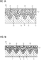
- Figure 1A shows a schematic sectional view of an electrical connection between a first contact 10 and a second contact 20 that has already been joined using the method according to the invention of the contact 10 are formed.
- the pins or rows of pins 11 are preferably arranged at regular intervals and particularly preferably in a square grid.
- the second contact 20 has an area 21 with a porous or foam-like, or more generally speaking, a soft, electrically conductive material compared to the pegs, into which the pegs 11 are already fully inserted.
- the material in the area 21 is partially displaced during the insertion of the pins, in particular in the partial areas 22 of the area 21 enclosing the pins 11, and in any case also partially compressed in the process.
- an at least slight, intentional deformation of the pins 11 during insertion into the area 21 take place.
- pins with a core made of a harder material can be covered with a soft(er) material in order to promote mutual deformation during the insertion process and to achieve better contact.
- the pins 11 are in the example Figure 1A essentially in the form of a circular cone, but can of course also assume other suitable shapes, for example cylindrical with a circular cross-section. However, other cross-sections such as ellipses, triangles, quadrilaterals, in particular squares, etc., can also be considered, which can also assume more complex shapes, which can therefore have tapers, undercuts or connections to one another (when viewed from the side). It is also possible to configure the pins in the form of a column or pillar, ie with a small diameter compared to the length, for example with a length of 2.0 mm and a diameter of 0.5 mm. In other configurations it is possible to choose tapered tenons, as in Figure 1A implied.
- the number, shape and dimensions of the pins can be freely selected within a wide range depending on the application and the manufacturing technology selected for the pins and the conductive material of the partner contact. It is thus possible, for example with only a low electrical or thermal load, to provide a few pins or just one pin. In other applications, however, it makes sense to use a large number of pegs, for example in order to increase the total contacting area, which increases with the number of pegs or pillars.
- the pegs can be made by various methods. For example, methods can be considered in which the respective contact 10 is produced with the pins 11 in one process step, ie for example embossing or die-casting methods, but also those described below Methods that are particularly suitable for producing studs or pillars directly on a semiconductor component.
- additive manufacturing processes are particularly useful there, but also galvanic manufacturing processes and thermal spraying processes and/or sintering processes, in particular with silver.
- thermal spraying process is used here as a generic term for the following processes, among others: application of material by atomization from a melt (melt pool spraying), application of material by electrical arc or gas discharge (e.g. arc spraying or plasma spraying), application of material by gas expansion without Combustion (e.g. cold gas spraying), application of material using combustion processes (e.g. wire flame spraying, powder flame spraying, high-velocity flame spraying, detonation spraying) or application of material using concentrated energetic beams (e.g. laser spraying).
- Cu, Ag, Au, Fe, Sn, Ni, Al, Mo, Wo or alloys of at least one of these elements come into consideration as material for the pins or pillars.
- semi-metals, metal-ceramics, highly doped semiconductors such as Si, SiC, GaN or graphite-based materials can also be used.
- the pegs or pillars can also be constructed from different material combinations, such as copper on one end of the pillar and graphite on the other end.
- the pegs can be plated with a metallic material or solder, for example Sn, Au, Ag.
- a metallic material or solder for example Sn, Au, Ag.
- Au oxide-free surface
- Sn soft metal
- the area 21 is in the in 1 example shown as uniform. In other embodiments, however, it is readily possible to divide the area provided for receiving the pins into sub-areas or connection islands which adjoin one another or can be separated by areas without soft material. It is also possible to equip these sub-areas with different soft material in order to ensure the contact quality over a wide temperature range, for example by choosing a soft material with good conductivity in a first, lower temperature range in a first sub-area and another in a second sub-area soft material is chosen with good conductivity in a second temperature range above the first temperature range.
- the contacts 10, 20 can be arranged on or on any circuit elements, connectors and the circuit carrier itself or formed integrally therewith (not shown).
- the circuit carrier can be a conventional Printed Circuit Board (PCB), an Active Metal Braze Substrate (AMB) or a Direct Copper Bond (DCB) carrier, one or more lead frames or an organic thick copper polymer substrate.
- Thick copper substrate means copper thicknesses of more than 0.3 mm, for example 1.0 mm, 2.0 mm or 4.0 mm.
- the circuit element can be an active or passive circuit element, in particular a power semiconductor.
- the circuit element can be applied to the carrier on the carrier side using the method described here or using a conventional method, for example by soldering or by sintering methods or by the method disclosed in the parallel patent application described in more detail above.
- a circuit element can have contacts of the type described here on one side or on several sides. In this case, the circuit element can only have contacts with pins or only contacts with soft areas as well as a combination of both types of contact.
- the contact that can be achieved after joining with only a low joining force is already sufficient, both for the electrical conductivity of the contact and for the thermal conductivity of the contact, as far as the thermal conductivity of the contact is concerned respective use case matters at all.
- the soft material 21 after joining it is advantageous to further compress the soft material 21 after joining.
- the result of the compression is in Figure 1B shown in a schematic sectional view.
- the compaction can be achieved by various measures. In particular, the following are possible: the exercise of a joint force with which the in Figure 1A condition shown is reached, exceeding compaction force; laser machining; heat treatment, preferably at temperatures lower than those encountered in soldering; delivery of energy by means of ultrasound; as well as suitable combinations of these measures, for example heating the joint before exerting a compression force.
- the entire area 21 and in particular the partial areas 22 enclosing the pegs 11 is compressed, as a result of which, for example, the electrical conductivity of the soft material and/or its temperature resistance can be improved.
- the pegs 11 and the contact 20 by suitably designing the pegs 11 and the contact 20 and in particular the area 21 equipped with material that is soft in relation to the peg material, it can be achieved that the pegs 11 are in direct mechanical and electrical contact with a harder base layer after compression of the soft material 21 (see also 2 ) of the contact 20 are, for example, to further increase the electrical conductivity and reliability of the contact.
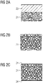
- the electrically conductive material 21 of the contact 20 which is soft compared to the pins and is applied to a flat carrier 23 which is harder in comparison, for example a metal sheet 23 .
- a gradual transition between the carrier and the porous material can be designed.
- the carrier and the soft material are delimited from one another largely without transitions.
- the connection with the pins takes place from below, ie on the side of the contact which has the soft material 21 .
- the contact 20 essentially consists of the porous or foam-like or soft, electrically conductive material 21 compared to the pin, ie the soft material 21 is selected so that it forms a mechanically stable contact 20 without a separate carrier, but is still soft compared to the pin material is enough to allow penetration of the studs (possibly using a tool that secures the shape of the contact 20) without deforming the contact 20 to the point of being unusable.
- the soft material 21 is selected so that it forms a mechanically stable contact 20 without a separate carrier, but is still soft compared to the pin material is enough to allow penetration of the studs (possibly using a tool that secures the shape of the contact 20) without deforming the contact 20 to the point of being unusable.
- it makes sense to compact the soft material 21 after it has been joined to the pins 11, as in connection with FIG Figure 1B already explained.
- Advantageous has the in Figure 2B
- the contact shown does not have a preferred mounting direction, so it can be joined to the pins from any
- a sandwich design for a contact 20 is shown, in which the porous or foam-like material 21 of the contact 20, which is soft relative to the pin, is embedded between two flat carriers 24, which consist of a material that is harder than the soft material and in which it can be sheet metal, for example.
- the thickness of the sheets 24 can be approximately the same, or a greater thickness and/or a harder material is selected for one of the sheets than for the other sheet. This more resistant sheet then forms the contact support, while the other sheet stabilizes and protects the soft material 21 .
- the assembly with the tenons is carried out on the side of the contact that has the less resistive sheet 24, the tenons being suitably shaped to pierce the less resistive sheet during the assembly operation, or with appropriate holes being made prior to assembly with the tenons be introduced into the less resistant sheet metal.
- the two sheets 24 are of approximately the same strength and are selected together with the soft material 21 in such a way that the combination of sandwich sheets 24 and soft material 21, which holds the sheets 24 together, ensures the desired mechanical properties of the contact 20.
- the joining with the pegs can take place from two directions, namely preferably perpendicular to the planes spanned by the metal sheets 24, in the representation of FIG Figure 2C i.e. from above and below.
- bent metal sheets at least partially cover the soft material enclose, and/or contacts in which several, preferably four, metal sheets enclose the soft material in the longitudinal direction (ie from left to right in the representation of the Figure 2C ) completely enclose, which then result in corresponding further contacting directions.
- "sandwich shape" is to be understood here as limited to two substantially parallel sheets 24 .
- the soft material 21 and, if necessary, the metal sheets 23, 24 are selected in such a way that the desired mechanical properties of the contact 20 are ensured.
- the contact 20 can be in the form of a contact tab protruding from the component, with corresponding requirements for flexibility combined with mechanical strength.
- the contact 20 can be arranged flat on a surface of the component and is mechanically stabilized by this surface or by the component itself.
- the soft material can be used as in Figure 2B shown without further layers or as in Figures 2A and 2C shown with limiting outer layers 23, 24 are used,
- a layer 23, 24 can act as a carrier material and can preferably consist of copper. It is used for mechanical stability and additional enlargement of the conductor cross-section.
- the side that is intended for joining with the pin(s) can be made thinner than a side that is not intended for joining.
- This joining side can in particular be made very thin in the manner of a skin and preferably consist of the same material as the soft material.
- asymmetrical sandwich designs are also possible, for example by applying a soft, porous or foam-like metal to a flat copper carrier, which has a flat outer skin, i.e. a thin layer, on the joining side, which is created during the manufacturing process, for example and is not subsequently removed or is applied in an additional manufacturing step.
- the exemplary embodiments of the present invention refer to power semiconductors, because reliable contacting that is as large as possible, as close as possible to the chip and therefore as possible without the supply of heat is of particular importance there.
- the invention is of course not limited to power semiconductors, but can be used in connection with all components that can be mounted on circuit carriers, either actively or passively.
Landscapes
- Connections Effected By Soldering, Adhesion, Or Permanent Deformation (AREA)
Priority Applications (1)
| Application Number | Priority Date | Filing Date | Title |
|---|---|---|---|
| EP21169988.9A EP4080564A1 (fr) | 2021-04-22 | 2021-04-22 | Contact électrique d'un élément de circuit applicable à un porte-circuit ou d'un connecteur électrique, ainsi que procédé d'établissement d'une connexion électriquement conductrice |
Applications Claiming Priority (1)
| Application Number | Priority Date | Filing Date | Title |
|---|---|---|---|
| EP21169988.9A EP4080564A1 (fr) | 2021-04-22 | 2021-04-22 | Contact électrique d'un élément de circuit applicable à un porte-circuit ou d'un connecteur électrique, ainsi que procédé d'établissement d'une connexion électriquement conductrice |
Publications (1)
| Publication Number | Publication Date |
|---|---|
| EP4080564A1 true EP4080564A1 (fr) | 2022-10-26 |
Family
ID=75674605
Family Applications (1)
| Application Number | Title | Priority Date | Filing Date |
|---|---|---|---|
| EP21169988.9A Withdrawn EP4080564A1 (fr) | 2021-04-22 | 2021-04-22 | Contact électrique d'un élément de circuit applicable à un porte-circuit ou d'un connecteur électrique, ainsi que procédé d'établissement d'une connexion électriquement conductrice |
Country Status (1)
| Country | Link |
|---|---|
| EP (1) | EP4080564A1 (fr) |
Citations (4)
| Publication number | Priority date | Publication date | Assignee | Title |
|---|---|---|---|---|
| US20140126165A1 (en) * | 2012-11-06 | 2014-05-08 | Infineon Technologies Austria Ag | Packaged Nano-Structured Component and Method of Making a Packaged Nano-Structured Component |
| DE102013219433A1 (de) * | 2013-09-26 | 2015-03-26 | Siemens Aktiengesellschaft | Elektronisches Leistungsmodul mit elastischen Kontakten und Stapelaufbau mit einem solchen Leistungsmodul |
| US20200006243A1 (en) * | 2017-03-24 | 2020-01-02 | Mitsubishi Electric Corporation | Semiconductor device and method of manufacturing same |
| WO2021013401A1 (fr) | 2019-07-25 | 2021-01-28 | Siemens Aktiengesellschaft | Procédé et arrangement dissipateur thermique pour le refroidissement de puces en semiconducteur avec circuits électroniques intégrés pour applications électroniques de puissance |
-
2021
- 2021-04-22 EP EP21169988.9A patent/EP4080564A1/fr not_active Withdrawn
Patent Citations (4)
| Publication number | Priority date | Publication date | Assignee | Title |
|---|---|---|---|---|
| US20140126165A1 (en) * | 2012-11-06 | 2014-05-08 | Infineon Technologies Austria Ag | Packaged Nano-Structured Component and Method of Making a Packaged Nano-Structured Component |
| DE102013219433A1 (de) * | 2013-09-26 | 2015-03-26 | Siemens Aktiengesellschaft | Elektronisches Leistungsmodul mit elastischen Kontakten und Stapelaufbau mit einem solchen Leistungsmodul |
| US20200006243A1 (en) * | 2017-03-24 | 2020-01-02 | Mitsubishi Electric Corporation | Semiconductor device and method of manufacturing same |
| WO2021013401A1 (fr) | 2019-07-25 | 2021-01-28 | Siemens Aktiengesellschaft | Procédé et arrangement dissipateur thermique pour le refroidissement de puces en semiconducteur avec circuits électroniques intégrés pour applications électroniques de puissance |
Non-Patent Citations (1)
| Title |
|---|
| "Applikationshandbuch Leistungshalbleiter", 2015, HERAUSGEBER SEMIKRON INTERNATIONAL GMBH |
Similar Documents
| Publication | Publication Date | Title |
|---|---|---|
| EP3262666B1 (fr) | Composant électrique et procédé de manufacture de ce composant | |
| DE69022605T2 (de) | Elektrische Verbindungsvorrichtung. | |
| DE2813968C2 (de) | Halbleiteranordnung | |
| CH652533A5 (de) | Halbleiterbaustein. | |
| EP2516321B1 (fr) | Capteur comportant un substrat céramique de préférence multicouche et procédé de fabrication correspondant | |
| DE19830820A1 (de) | Elektronisches Keramikbauteil und Verfahren zum Herstellen des elektronischen Keramikbauteils | |
| EP1208573B1 (fr) | Anode pour condensateurs electrolytiques, condensateur electrolytique et procedes de production de l'anode | |
| EP1502310A2 (fr) | Piezoactionneur et son procede de production | |
| DE19924341A1 (de) | Elektronisches Keramikbauteil und eine Anbringungsstruktur für dasselbe | |
| EP2649864A1 (fr) | Carte de circuits imprimés | |
| DE102014105000B4 (de) | Verfahren zur Herstellung und zum Bestücken eines Schaltungsträgers | |
| EP3229566A1 (fr) | Élément de liaison pour une système de composant électronique et son procédé de fabrication et système de composant et son procédé de production | |
| DE4015463A1 (de) | Verfahren zum anbringen von leitenden anschluessen an keramikkomponenten | |
| DE19523977A1 (de) | Microchip-Sicherung | |
| DE102010022925B4 (de) | Piezoelektrisches Vielschichtbauelement und Verfahren zur Ausbildung einer Außenelektrode bei einem piezoelektrischen Vielschichtbauelement | |
| DE10103084B4 (de) | Halbleitermodul und Verfahren zu seiner Herstellung | |
| DE2004776A1 (de) | Halbleiterbauelement | |
| WO2004073013A2 (fr) | Composant electronique dote d'une puce a semi-conducteurs, notamment module de puissance haute frequence et procede de fabrication associe | |
| EP1741162A2 (fr) | Unite fonctionnelle electrique et procede pour sa production | |
| DE112020003541T5 (de) | Leistungshalbleitermodul | |
| EP1714328A2 (fr) | Actionneur piezo-electrique et procede de production correspondant | |
| DE102009044933B4 (de) | Leistungshalbleitermodul mit mindestens zwei verbundenen Schaltungsträgern und Verfahren zur Herstellung eines Leistungshalbleitermoduls mit mindestens zwei verbundenen Schaltungsträgern | |
| EP4282034B1 (fr) | Dispositif connecteur d'alimentation pour cartes de circuit imprimé et procédé de montage d'un tel dispositif connecteur d'alimentation sur une carte de circuit imprimé | |
| DE102021117573B4 (de) | Verfahren zur Herstellung einer elektrischen Verbindung zu einem elektronischen Bauteil und einer Chip-Baugruppe | |
| EP4080563A1 (fr) | Élément de circuit applicable à un porte-circuit, connecteur électrique, ainsi que procédé d'établissement d'une connexion électrique |
Legal Events
| Date | Code | Title | Description |
|---|---|---|---|
| PUAI | Public reference made under article 153(3) epc to a published international application that has entered the european phase |
Free format text: ORIGINAL CODE: 0009012 |
|
| STAA | Information on the status of an ep patent application or granted ep patent |
Free format text: STATUS: THE APPLICATION HAS BEEN PUBLISHED |
|
| AK | Designated contracting states |
Kind code of ref document: A1 Designated state(s): AL AT BE BG CH CY CZ DE DK EE ES FI FR GB GR HR HU IE IS IT LI LT LU LV MC MK MT NL NO PL PT RO RS SE SI SK SM TR |
|
| STAA | Information on the status of an ep patent application or granted ep patent |
Free format text: STATUS: THE APPLICATION IS DEEMED TO BE WITHDRAWN |
|
| 18D | Application deemed to be withdrawn |
Effective date: 20230427 |