EP4080680A1 - Antennenvorrichtung - Google Patents
Antennenvorrichtung Download PDFInfo
- Publication number
- EP4080680A1 EP4080680A1 EP21751015.5A EP21751015A EP4080680A1 EP 4080680 A1 EP4080680 A1 EP 4080680A1 EP 21751015 A EP21751015 A EP 21751015A EP 4080680 A1 EP4080680 A1 EP 4080680A1
- Authority
- EP
- European Patent Office
- Prior art keywords
- antenna device
- antenna
- transparent cover
- electronic apparatus
- antenna element
- Prior art date
- Legal status (The legal status is an assumption and is not a legal conclusion. Google has not performed a legal analysis and makes no representation as to the accuracy of the status listed.)
- Pending
Links
Images


Classifications
-
- H—ELECTRICITY
- H01—ELECTRIC ELEMENTS
- H01Q—ANTENNAS, i.e. RADIO AERIALS
- H01Q1/00—Details of, or arrangements associated with, antennas
- H01Q1/12—Supports; Mounting means
- H01Q1/22—Supports; Mounting means by structural association with other equipment or articles
- H01Q1/24—Supports; Mounting means by structural association with other equipment or articles with receiving set
- H01Q1/241—Supports; Mounting means by structural association with other equipment or articles with receiving set used in mobile communications, e.g. GSM
- H01Q1/242—Supports; Mounting means by structural association with other equipment or articles with receiving set used in mobile communications, e.g. GSM specially adapted for hand-held use
- H01Q1/243—Supports; Mounting means by structural association with other equipment or articles with receiving set used in mobile communications, e.g. GSM specially adapted for hand-held use with built-in antennas
-
- H—ELECTRICITY
- H01—ELECTRIC ELEMENTS
- H01Q—ANTENNAS, i.e. RADIO AERIALS
- H01Q1/00—Details of, or arrangements associated with, antennas
- H01Q1/08—Means for collapsing antennas or parts thereof
- H01Q1/085—Flexible aerials; Whip aerials with a resilient base
-
- H—ELECTRICITY
- H01—ELECTRIC ELEMENTS
- H01Q—ANTENNAS, i.e. RADIO AERIALS
- H01Q1/00—Details of, or arrangements associated with, antennas
- H01Q1/36—Structural form of radiating elements, e.g. cone, spiral, umbrella; Particular materials used therewith
- H01Q1/364—Structural form of radiating elements, e.g. cone, spiral, umbrella; Particular materials used therewith using a particular conducting material, e.g. superconductor
-
- H—ELECTRICITY
- H01—ELECTRIC ELEMENTS
- H01Q—ANTENNAS, i.e. RADIO AERIALS
- H01Q1/00—Details of, or arrangements associated with, antennas
- H01Q1/36—Structural form of radiating elements, e.g. cone, spiral, umbrella; Particular materials used therewith
- H01Q1/38—Structural form of radiating elements, e.g. cone, spiral, umbrella; Particular materials used therewith formed by a conductive layer on an insulating support
-
- H—ELECTRICITY
- H01—ELECTRIC ELEMENTS
- H01Q—ANTENNAS, i.e. RADIO AERIALS
- H01Q1/00—Details of, or arrangements associated with, antennas
- H01Q1/44—Details of, or arrangements associated with, antennas using equipment having another main function to serve additionally as an antenna, e.g. means for giving an antenna an aesthetic aspect
-
- H—ELECTRICITY
- H01—ELECTRIC ELEMENTS
- H01Q—ANTENNAS, i.e. RADIO AERIALS
- H01Q19/00—Combinations of primary active antenna elements and units with secondary devices, e.g. with quasi-optical devices, for giving the antenna a desired directional characteristic
- H01Q19/28—Combinations of primary active antenna elements and units with secondary devices, e.g. with quasi-optical devices, for giving the antenna a desired directional characteristic using a secondary device in the form of two or more substantially straight conductive elements
- H01Q19/30—Combinations of primary active antenna elements and units with secondary devices, e.g. with quasi-optical devices, for giving the antenna a desired directional characteristic using a secondary device in the form of two or more substantially straight conductive elements the primary active element being centre-fed and substantially straight, e.g. Yagi antenna
-
- H—ELECTRICITY
- H01—ELECTRIC ELEMENTS
- H01Q—ANTENNAS, i.e. RADIO AERIALS
- H01Q11/00—Electrically-long antennas having dimensions more than twice the shortest operating wavelength and consisting of conductive active radiating elements
- H01Q11/02—Non-resonant antennas, e.g. travelling-wave antenna
- H01Q11/10—Logperiodic antennas
- H01Q11/105—Logperiodic antennas using a dielectric support
-
- H—ELECTRICITY
- H01—ELECTRIC ELEMENTS
- H01Q—ANTENNAS, i.e. RADIO AERIALS
- H01Q13/00—Waveguide horns or mouths; Slot antennas; Leaky-waveguide antennas; Equivalent structures causing radiation along the transmission path of a guided wave
- H01Q13/08—Radiating ends of two-conductor microwave transmission lines, e.g. of coaxial lines, of microstrip lines
- H01Q13/085—Slot-line radiating ends
-
- H—ELECTRICITY
- H01—ELECTRIC ELEMENTS
- H01Q—ANTENNAS, i.e. RADIO AERIALS
- H01Q13/00—Waveguide horns or mouths; Slot antennas; Leaky-waveguide antennas; Equivalent structures causing radiation along the transmission path of a guided wave
- H01Q13/10—Resonant slot antennas
- H01Q13/106—Microstrip slot antennas
-
- H—ELECTRICITY
- H01—ELECTRIC ELEMENTS
- H01Q—ANTENNAS, i.e. RADIO AERIALS
- H01Q9/00—Electrically-short antennas having dimensions not more than twice the operating wavelength and consisting of conductive active radiating elements
- H01Q9/04—Resonant antennas
- H01Q9/06—Details
- H01Q9/065—Microstrip dipole antennas
-
- H—ELECTRICITY
- H01—ELECTRIC ELEMENTS
- H01Q—ANTENNAS, i.e. RADIO AERIALS
- H01Q9/00—Electrically-short antennas having dimensions not more than twice the operating wavelength and consisting of conductive active radiating elements
- H01Q9/04—Resonant antennas
- H01Q9/30—Resonant antennas with feed to end of elongated active element, e.g. unipole
Definitions
- the present invention relates to an antenna device.
- a conventional antenna device used for an electronic apparatus such as a smartphone, which includes a ground plane, a sheet conductor that has a section that faces the ground plane with a gap therebetween, a feed element connected to a feeding point with the ground plane serving as the ground therefor, and a linear radiating element connected to the sheet conductor, wherein the feed element supplies power to the radiating element in a contactless manner, so that the radiating element functions as a radiating conductor (for example, see Patent Literature 1.).
- the conventional antenna device is not suitable for the arrangement at the position visible from the outside of a transparent cover of the electronic apparatus because the arrangement at the position visible from the outside of the transparent cover of the electronic apparatus reduces the visibility of the display panel.
- An antenna device includes a flexible substrate that is transparent and that is to be provided on an inner surface side opposite to an outer surface of a transparent cover, made of glass or resin, of an electronic apparatus, and an antenna element that is transparent and that is to be provided at a position, of the flexible substrate, that is visible from outside of the transparent cover, the antenna element having a directivity oriented toward an outside of the electronic apparatus.
- An antenna device including a transparent antenna element that can be provided at a position visible from the outside of a transparent cover of an electronic apparatus can be provided.
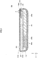
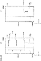
- FIG. 1 is a drawing illustrating an example of a cross-section of an electronic apparatus 200 including an antenna device 100.
- FIG. 2 is an enlarged view of a portion of a cross-section of the electronic apparatus 200.
- an XYZ coordinate system is defined for explanation.
- a plan view refers to a view in the YZ plane.
- an up-and-down direction in which +X direction side is the upper side and -X direction side is the lower side and a lateral direction (sideways) with respect to the up-and-down direction are used, but they do not represent the universal up-and-down direction and horizontal directions.
- an X axis direction, a Y axis direction, and a Z axis direction represent a direction parallel to the X axis, a direction parallel to the Y axis, and a direction parallel to the Z axis, respectively.
- the X axis direction, the Y axis direction, and the Z axis direction are orthogonal to each other.
- the XY plane, the YZ plane, and the ZX plane are a virtual plane parallel to the X axis direction and the Y axis direction, a virtual plane parallel to the Y axis direction and the Z axis direction, and a virtual plane parallel to the Z axis direction and the X axis direction, respectively.
- the antenna device 100 is suitable for transmitting and receiving electromagnetic waves of a high frequency band (For example, over 1 GHz to 300 GHz) such as microwave or millimeter wave.
- the antenna device 100 is applicable to a fifth generation mobile communication system (5G), a sixth generation mobile communication system (6G), or the like as an example, but the applicable system is not limited thereto.
- the fifth generation mobile communication system (5G) includes, for example, a 28 GHz band and a band less than 6 GHz (Sub6).
- FIGs. 1 and 2 illustrate a portion 100A and a portion 100B of the antenna device 100.
- the portion 100A is an example of a first portion
- the portion 100B is an example of a second portion of the antenna device 100.
- the portion 100A is illustrated in white with an outline
- the portion 100B is illustrated in gray.
- the antenna device 100 includes, for example, a flexible substrate, an antenna element, and a feeding line, and is bendable.
- the antenna device 100 is bent to be folded between the portion 100A and the portion 100B.
- the portion 100B is further bent in the inside of a storing portion 210B.
- the portion 100A is a portion where at least an antenna element is provided on the flexible substrate, and not only the antenna element but also a portion of the feeding line may be provided in the portion 100A.
- the portion 100B is a portion where at least a portion of the feeding line (the entire feeding line or the remaining portion of the feeding line other than a portion provided in the portion 100A) is provided on the flexible substrate.
- the portion 100A of the antenna device 100 is provided on the upper side (display surface side) of a display panel included in a display operation unit 230.
- the portion 100A of the antenna device 100 is transparent because it is visible from the outside of the electronic apparatus 200 through the transparent cover 220.
- the portion 100B is provided on the rear side of the display operation unit 230 and is not visible from the outside of the electronic apparatus 200, and therefore, the portion 100B does not have to be transparent.
- the portion 100A of the antenna device 100 is illustrated between the transparent cover 220 and the display operation unit 230 for the convenience of explanation, but the portion 100A of the antenna device 100 is not limited to be provided between the display operation unit 230 and the transparent cover 220, and may be provided between any of a touch panel, a polarizing plate, and a display panel included in the display operation unit 230.
- the positional relationship between the portion 100A of the antenna device 100, the transparent cover 220, and the display operation unit 230 is described later.
- the antenna device 100 has a directivity toward the outside of the electronic apparatus 200.
- the directivity of the antenna device 100 is the directivity of the main lobe.
- the directivity toward the outside means that the directivity of the main lobe of the antenna device 100 is oriented toward the outside of a housing 210 and the transparent cover 220 of the electronic apparatus 200.
- "Oriented toward the outside” means that, for example, the directivity is oriented toward, as seen from the inside of the electronic apparatus 200, +X direction of the transparent cover 220, a direction parallel to the YZ plane on the outside of the transparent cover 220, a direction between the +X direction of the transparent cover 220 and the direction parallel to the YZ plane on the outside of the transparent cover 220, or the like.
- the housing may face the outside of the housing 210 through the portion made of the dielectric material.
- the electronic apparatus 200 is, for example, an information processing terminal such as a smart phone, a tablet computer, or a notebook PC (Personal Computer).
- the electronic apparatus 200 is not limited to these, and may be, for example, a structure such as a pillar or a wall, a digital signage, an electronic apparatus including a display panel in a train, or an electronic apparatus including various display panels in a vehicle.
- the electronic apparatus 200 includes, in addition to the antenna device 100, the housing 210, the transparent cover 220, the display operation unit 230, a circuit board 240, electronic components 250A and 250B, a battery 260, and the like.
- the display operation unit 230 has a display panel.
- the electronic apparatus 200 may be an electronic apparatus that includes the housing 210, the transparent cover 220, and the display panel.
- the housing 210 is a case made of, for example, metal and/or resin and covers the lower surface and the side surface of the electronic apparatus 200.
- the housing 210 has an opening portion 210A on the upper side, and a transparent cover 220 is attached to the opening portion 210A.
- the housing 210 has a storing portion 210B which is an internal space in communication with the opening portion 210A.
- the circuit board 240, electronic components 250A and 250B, the battery 260, and the like are accommodated in the storing portion 210B.
- the transparent cover 220 is a transparent glass plate in a rectangular shape in a plan view, and has a size matching the opening portion 210A in a plan view.
- the transparent cover 220 is, for example, a flat glass plate.
- the transparent cover 220 is made of glass in this explanation, the transparent cover 220 may be made of resin.
- the transparent cover 220 When the transparent cover 220 is attached to the opening portion 210A of the housing 210, the storing portion 210B of the housing 210 is sealed.
- the upper surface of the transparent cover 220 is an example of an outer surface of the transparent cover 220, and the lower surface of the transparent cover 220 is an example of an inner surface of the transparent cover 220.
- the display operation unit 230 is provided on the inner surface side of the transparent cover 220. From the outside of the electronic apparatus 200, the display operation unit 230 provided inside is visible through the transparent cover 220.
- the display operation unit 230 is a composite object made by stacking a touch panel, a polarizing plate, a display panel, and the like.
- the electronic apparatus 200 allows GUI (Graphical User Interface) buttons and the like displayed on the display panel of the display operation unit 230 to be operated by touching the upper surface of the transparent cover 220. The user's operation is detected by the touch panel of the display operation unit 230.
- GUI Graphic User Interface
- the display panel is provided at the lowest side of the display operation unit 230.
- the touch panel and the polarizing plate are stacked on the display panel.
- the order in which the touch panel and the polarizing plate are stacked is not particularly limited.
- the antenna device 100 is provided at any position on the upper side of the display panel.
- the electronic components 250A, 250B are mounted on the circuit board 240.
- a feeding line or the like of a portion 100B of the antenna device 100 is connected to the circuit board 240.
- the circuit board 240 and the portion 100B may be connected by a connector, an ACF (Anisotropic Conductive Film), or the like, or may be connected by other components.
- the electronic component 250A is a component that performs information processing related to the operation of the electronic apparatus 200, and is implemented by a computer including, for example, a CPU (central processing unit), RAM (random access memory), ROM (read only memory), HDD (hard disk drive), an input and output interface, an internal bus, and the like.
- a CPU central processing unit
- RAM random access memory
- ROM read only memory
- HDD hard disk drive
- the electronic component 250B is, for example, a communication module connected to the portion 100B of the antenna device 100 via a wiring of the circuit board 240 and configured to process signals transmitted or received via the antenna device 100.
- the battery 260 is a rechargeable secondary battery and supplies power necessary for the operation of the antenna device 100, the display operation unit 230, and the electronic components 250A, 250B, and the like.
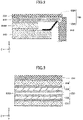
- FIG. 3 is an enlarged view of the broken line portion A of FIG. 1 .
- the display operation unit 230 has a display panel 231, a layer 232, a layer 233, and an adhesive layer 234.
- the adhesive layer 234 is a layer made of an adhesive that is provided for bonding the display operation unit 230 to the transparent cover 220.
- the display panel 231 is, for example, a liquid crystal display panel, an organic EL (electroluminescence) display panel, or an OLED (organic light emitting diode) display panel, and is arranged on the lowest side of the display operation unit 230.
- the layers 232 and 233 include at least a touch panel, a polarization plate, and a plurality of adhesive layers.
- the layer 232 may include a touch panel and an adhesive layer, and the layer 233 may include a polarization plate and an adhesive layer.
- the layer 232 may include a polarizing plate and an adhesive layer, and the layer 233 may include a touch panel and an adhesive layer.
- the portion 100A of the antenna device 100 is illustrated between the layers 232 and 233, but the portion 100A may be disposed between the layer 233 and the adhesive layer 234 or between the layer 232 and the display panel 231.
- the cross-sectional structure of the transparent cover 220 and the display operation unit 230 is a structure in which the portion 100A of the antenna device 100 is removed from FIG. 3 .
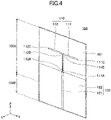
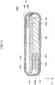
- FIGs. 4 and 5 are drawings illustrating the antenna device 100.
- FIGs. 4 and 5 illustrate a state before the portion 100B is bent in parallel with the YZ plane as illustrated in FIGs. 1 and 2 .
- the antenna device 100 includes a substrate 101, an antenna element 110, and a microstrip line 120.
- FIG. 5 (A) illustrates the substrate 101 and the components provided on the surface of the substrate 101 on the +X direction side
- FIG. 5 (B) illustrates the components provided on the surface of the substrate 101 on the +X direction side.
- the position of the substrate 101 is indicated by a broken line.
- the portion of the microstrip line 120 that is included in the portion 100A is, for example, about 1/2 to 3/4, on the +Z direction side, of the entirety of the microstrip line 120 in the Z direction. Therefore, the portion of the microstrip line 120 that is included in the portion 100B is, for example, about 1/4 to 1/2 of the entirety of the microstrip line 120 in the Z direction.
- the boundary between the portions 100A and 100B illustrated in FIGs. 1 and 2 is about 1/2 to 3/4 from the end portion, on the +Z direction side, of the microstrip line 120 in the Z direction. Since the portion 100B is situated over the display panel 231 illustrated in FIG. 3 , the portion 100B may be transparent to avoid reducing the visibility. The portion 100B does not have to be transparent.
- FIGs. 4 and 5 illustrate, for example, a configuration in which the boundary between the portions 100A and 100B is 1/2 from the end portion, on the +Z direction side, of the microstrip line 120 in the Z direction.
- the substrate 101 is, for example, a flexible substrate made of polyimide and can be bent in the Z direction and/or the Y direction.
- the substrate 101 is colorless and transparent.
- the antenna element 110 is a dipole type antenna and has elements 111 and 112.
- the element 111 is provided on the surface of the substrate 101 on the +X direction side, and is an L-shaped element having a feeding point 111A, a bent portion 111B, and an open end 111C.
- the element 111 extends from the feeding point 111A toward the bent portion 111B in the +Z direction, is bent in the +Y direction at the bent portion 111B, and extends to the open end 111C.
- the element 112 is an L-shaped element provided on the surface of the substrate 101 on the -X direction side, and includes a feeding point 112A, a bent portion 112B, and an open end 112C.
- the section between the feeding point 112A and the bent portion 112B is superposed in a plan view on the section between the feeding point 112A and the bent portion 112B of the element 111, and the section between the bent portion 112B and the open end 112C extends in the -Y direction in a direction opposite to the section between the bent portion 111B and the open end 111C of the element 111.
- the length in the Y direction between the open end 111C and the open end 112C is set to be about 1/2 of the electric length ⁇ e of the wavelength ⁇ (i.e., ⁇ e/2) at the resonance frequency of the antenna device 100.
- the microstrip line 120 is a feeding line including a transmission line 121 and a ground layer 122.
- the transmission line 121 is provided on the surface of the substrate 101 on the +X direction side, and is connected to the feeding point 111A of the element 111.
- the ground layer 122 is provided to be stacked on the transmission line 121 in a plan view on the surface of the substrate 101 on the -X direction side. An edge of the ground layer 122 on the +Z direction side is connected to the feeding point 112A of the element 112.
- the section in the Z direction where the antenna element 110 and the portion of the microstrip line 120 on the +Z direction side is provided is the portion 100A illustrated in FIGs. 1 and 2 .
- a section of the antenna device 100 in the Z direction where the remaining portion of the microstrip line 120 is provided is the portion 100B illustrated in FIGs. 1 and 2 .
- the substrate 101 of the antenna device 100 is bent at a position between the end of the antenna element 110 and an end portion of the ground layer 122 on a side away from the antenna element 110.
- FIG. 6 is a drawing illustrating the transparent conductor 300A.
- the transparent conductor 300A is formed on the surface of the transparent substrate 101, and is used, for example, as the antenna element 110 and the microstrip line 120 included in the portion 100A illustrated in FIGs. 4 and 5 .
- the transparent conductor 300A is a conductor having such a high light transmittance that it is difficult to see the transparent conductor 300A with human visual acuity.
- the transparent conductor 300A is, for example, a conductive line in a mesh form in order to increase light transmittance.
- “mesh” means a state in which through holes 301 in a form of mesh are formed in the transparent conductor 300A.
- the openings of the mesh may be in a rectangular or rhomboid shape.
- the openings of the mesh are preferably in a square shape.
- the design is good.
- the openings of the mesh may be in self assembly-based random shapes. Such random shapes can prevent moiré.
- the line widths w1, w2 of the mesh are preferably 1 to 10 ⁇ m.
- the line gaps p1, p2 of the mesh are preferably 300 to 500 ⁇ m.
- the aperture ratio of the transparent conductor 300A is preferably 80% or more and more preferably 90% or more.
- the aperture ratio is a ratio of an area of aperture portions to a certain area of the transparent conductor 300A including the aperture portions (the through holes 301).
- the visible light transmittance of the transparent conductor 300A can be increased in accordance with an increase in the aperture ratio of the transparent conductor 300A.
- the thickness of the transparent conductor 300A is preferably 400 nm or less and more preferably 300 nm or less.
- the lower limit of the thickness of the transparent conductor 300A is not particularly limited, but may be 2 nm or more, may be 10 nm or more, or may be 30 nm or more in order to improve the radiation characteristics.
- the thickness of the transparent conductor 300A may be 1 to 40 ⁇ m. In a case where the transparent conductor 300A is formed in a mesh form, the visible light transmittance can be increased even when the transparent conductor 300A is thick.
- the thickness of the transparent conductor 300A is more preferably 5 ⁇ m or more and still more preferably 8 ⁇ m or more.
- the thickness of the transparent conductor 300A is more preferably 30 ⁇ m or less, still more preferably 20 ⁇ m or less, and particularly more preferably 15 ⁇ m or less.
- the conductive material of the transparent conductor 300A may be copper, but other materials such as gold, silver, platinum, aluminum, and chromium may be used, and the conductive material is not limited to these materials.
- the conductors such as the antenna element 110 and the microstrip line 120 included in the portion 100A may be implemented by the transparent conductor 300A, for example.
- the antenna element 110 implemented by the transparent conductor 300A and a portion of the microstrip line 120 are an antenna element and a feeding line, respectively, that are transparent and have such a high light transmittance that it is difficult to see the antenna element 110 and the microstrip line 120 with human visual acuity.
- the remaining portion of the microstrip line 120 included in the portion 100B of the antenna device 100 is located on the rear side of the display panel 231 (see FIG. 3 ), the remaining portion does not have to be transparent, and may be a solid pattern of copper and the like.
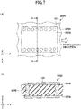
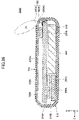
- FIG. 7 is a drawing illustrating the waveguide 300B formed on the substrate 101.
- FIG. 7 (A) illustrates the waveguide 300B in a plan view
- FIG. 7 (B) illustrates a cross section taken along arrow A-A of FIG. 7 (A) .
- an XYZ coordinate system is defined as illustrated for example.
- the waveguide 300B is formed in the substrate 101 and includes conductive layers 301B and 302B and through holes (THs) 303B.
- the waveguide 300B is what is termed as a SIW (Substrate Integrated Waveguide) including: the conductive layers 301B and 302B provided on both surfaces of the single-layer substrate 101; and the THs 303B.
- SIW Substrate Integrated Waveguide
- the conductive layers 301B and 302B are solid patterns (solid patterns) formed in a portion of the area between the surface on the -X direction side and the surface on the +X direction side of the substrate 101.
- the conductive layers 301B and 302B are provided on both surfaces of the substrate 101 with the same size in a plan view and aligned with each other.
- the TH 303B is a conductor in a column or tube shape that is formed inside the through hole penetrating the substrate 101 in the X direction by plating or the like.
- the THs 303B connect the conductive layers 301B and 302B.
- the THs 303B are provided at equal intervals on both sides of the conductive layers 301B and 302B along the propagation direction of the electromagnetic waves (in this case, for example, +Z direction) .
- the gap between the adjacent THs 303B in the Z direction is set to be less than the wavelength of the propagating electromagnetic waves.
- the space surrounded by the conductive layers 301B and 302B and the THs 303B can be shielded.
- the space surrounded by the conductive layers 301B and 302B and the THs 303B is a shielded transmission line, which can trap electromagnetic waves and allow the electromagnetic waves to propagate in the Z direction.
- the waveguide 300B described above may be used as a feeding line in the portion 100B (see FIGs. 1 and 2 ) of the antenna device 100 instead of the remaining portion of the microstrip line 120.
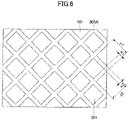
- FIG. 8 is a diagram illustrating frequency characteristics of the S11 parameter of the antenna device 100.
- FIG. 8 illustrates frequency characteristics of the S11 parameter obtained by an electromagnetic field simulation performed by setting the resonance frequency of the antenna device 100 to 28 GHz. Good characteristics were obtained in which the S11 parameter was not greater than -5 dB over a wide range around 28 GHz.
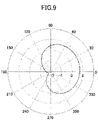
- FIG. 9 illustrates the directivity obtained by an electromagnetic field simulation performed by setting the resonance frequency of the antenna device 100 to 28 GHz.
- the directivity illustrated in FIG. 9 is the directivity of the main lobe of the antenna device 100.
- the direction of 0 degrees corresponds to the +Z direction
- the direction of 90 degrees corresponds to the +X direction.
- FIG. 9 it can be understood that the directivity in the +Z direction (the direction of 0 degrees) was obtained.
- FIG. 10 is a diagram illustrating the directivity of the antenna device 100 in an example of a cross section of the electronic apparatus 200.
- the directivity illustrated in FIG. 9 indicates that electromagnetic waves can be radiated in the direction indicated by (1) in FIG. 10 and electromagnetic waves in the direction indicated by (1) can be received.
- the direction indicated by (1) is a direction in which radiation is emitted from the surface of the transparent cover 220 of the electronic apparatus 200 (the surface of the electronic apparatus 200) along the surface of the transparent cover 220. Since the antenna device 100 has the directivity oriented in the direction (1), the antenna device 100 can communicate with a communication device external to the electronic apparatus 200.
- the antenna device 100 has a configuration in which the transparent antenna element 110 is provided on the transparent substrate 101.
- the transparent antenna element 110 is provided at a position visible from the outside of the transparent cover 220, and is stacked on the display panel 231 (see FIG. 3 ).
- the antenna device 100 can be provided that includes the transparent antenna element 110 that can be provided at a position visible from the outside of the transparent cover 220 of the electronic apparatus 200, the transparent portion of the microstrip line 120 that is included in the portion 100A, and the transparent substrate 101.
- the antenna element 110 of the dipole type and the microstrip line 120 can be formed very thin.
- the allowable thickness of the antenna device 100 is greatly limited, e.g., 100 ⁇ m or less, it is difficult to use an antenna device such as a patch antenna which requires a certain thickness for the ground layer.
- the antenna device 100 including the dipole antenna element 110 and the microstrip line 120, which can be formed very thin, is very advantageous from the viewpoint of reduction in the thickness.
- the transparent cover 220 of the electronic apparatus 200 is in the form of a flat plate, the transparent cover 220 may be curved.
- the antenna element 110 may be a monopole antenna, a tapered slot antenna, a slot antenna, or a log periodic antenna.
- the antenna device 100 may further include one or more parasitic elements that are fed via the antenna element 110.
- the directivity toward the outside of the electronic apparatus 200 may be achieved by adjusting the positional relationship between the antenna element 110 and one or more parasitic elements.
- FIG. 11 is a cross sectional view illustrating an electronic apparatus 200A according to a modified embodiment of the embodiment.
- FIG. 11 illustrates a cross section corresponding to FIG. 1 .
- the electronic apparatus 200A includes a transparent cover 220A and a display operation unit 230A having curved end portions in a plan view instead of the flat transparent cover 220 and the display operation unit 230 of the electronic apparatus 200 illustrated in FIG. 1 .
- the portion 100A is illustrated in white with an outline, and the portion 100B is illustrated in gray.
- both ends of the transparent cover 220 in the Z direction are curved in the -X direction. This is also applicable to the YZ cross section.
- the display operation unit 230A includes an OLED as a display panel for example, and has a curved shape similar to that of the transparent cover 220A.
- the portion 100A of the antenna device 100 is provided over the flat upper surface portion and the curved portion of the transparent cover 220A.
- the portion 100A of the antenna device 100 is illustrated between the transparent cover 220A and the display operation unit 230A, but the portion 100A of the antenna device 100 is not limited to be provided between the display operation unit 230A and the transparent cover 220A, but may be disposed between the layers 232 and 233 illustrated in FIG. 3 , between the layer 233 and the adhesive layer 234, or between the layer 232 and the display panel 231.
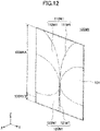
- the electronic apparatus 200 or 200A may include an antenna device 100M1 illustrated in FIGs. 12 and 13 instead of the antenna device 100 illustrated in FIGs. 4 and 5 .
- FIGs. 12 and 13 are drawings illustrating the antenna device 100M1.
- FIGs. 12 and 13 are drawings illustrating the antenna device 100M1.
- FIGs. 12 and 13 illustrate the antenna device 100M1 in a state before being bent in parallel with the YZ plane.
- the antenna device 100M1 includes portions 100M1A and 100M1B.
- the portions 100M1A and 100M1B are similar to the portions 100A and 100B illustrated in FIGs. 1 , 2 , 4 , and 5 .
- the portion 100M1A is visible from the outside of the electronic apparatus 200 or 200A via the transparent cover 220 or 220A of the electronic apparatus 200 or 200A.
- the portion 100M1B is situated on the rear side of the display operation unit 230 or 230A and is a portion that is not visible from the outside of the electronic apparatus 200 or 200A.
- FIGs. 12 and 13 illustrate, for example, a configuration in which the boundary between the portion 100M1A and the portion 100M1B is 1/2 from the end portion, on the +Z direction side, of the microstrip line 120M1 in the Z direction.
- the antenna device 100M1 includes a substrate 101, an antenna element 110M1, and a microstrip line 120M1.
- FIG. 13 (A) illustrates the substrate 101 and components provided on the surface of the substrate 101 on the +X direction side
- FIG. 13 (B) illustrates components provided on the surface of the substrate 101 on the +X direction side.
- the position of the substrate 101 is indicated by a broken line.
- the antenna element 110M1 is a Vivaldi antenna and has elements 111M1 and 112M1.
- the antenna element 110 M1 is implemented by a transparent conductor 300A (see FIG. 6 ).
- the element 111M1 is provided on the surface of the substrate 101 on the +X direction side, and includes a feeding point 111M1A and an open end 111M1C.
- the element 111M1 extends from the feeding point 111M1A to the open end 111M1C.
- the element 112M1 is provided on the surface of the substrate 101 on the -X direction side, and includes a feeding point 112M1A and an open end 112M1C.
- the feeding point 112M1A is superposed on the feeding point 111M1A of the element 111M1 in a plan view.
- the shape, size, and position of the element 112M1 relative to the substrate 101 as viewed in the -X direction is equal to the shape, size, and position of the element 111M1 relative to the substrate 101 as viewed in the +X direction.
- the microstrip line 120M1 has transmission lines 121M1A, 121M1B and ground layers 122M1A, 122M1B.
- the transmission lines 121M1A and 121M1B are provided on the surface of the substrate 101 on the +X direction side.
- the transmission line 121M1A is stacked on the ground layer 122M1A.
- the transmission line 121M1B is connected to the +Z direction side of the transmission line 121M1A, provided to be stacked on the ground layer 122M1B, and connected to the feeding point 111M1A of the element 111M1.
- the ground layer 122M1A is a ground pattern in a rectangular shape that is provided on the surface of the substrate 101 on the -X direction side so as to be superposed on the transmission line 121M1A in a plan view.
- the ground layer 122M1B is continuously formed on the +Z direction side of the ground layer 122M1A, and the width of the ground layer in the Y direction gradually decreases toward the +Z direction side.
- the end of the ground layer 122M1B in the +Z direction is situated at the center of the substrate 101 in the Y direction, and the width in the Y direction of the end portion of the ground layer 122M1B on the +Z direction side is equal to the width in the Y direction of the feeding point 112M1A of the element 112M1.
- the end portion of the ground layer 122M1B on the +Z direction side is connected to the feeding point 112M1A of the element 112M1.
- a portion in the Z direction where the antenna element 110M1 and a portion of the microstrip line 120M1 on the +Z direction side are provided is the portion 100A illustrated in FIGs. 1 and 2 .
- a section of the antenna device 100M1 where the remaining portion of the microstrip line 120M1 is provided is the portion 100B illustrated in FIGs. 1 and 2 . Since the portion 100A is situated over the display panel 231 illustrated in FIG. 3 , the portion 100A may be transparent to avoid obstructing the display.
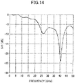
- FIG. 14 is a diagram illustrating frequency characteristics of the S11 parameter of the antenna device 100M1.
- FIG. 14 illustrates frequency characteristics of the S11 parameter obtained by an electromagnetic field simulation performed by setting the resonance frequency of the antenna device 100M1 to 28 GHz.
- An adequate bandwidth in which the S11 parameter becomes -5 dB or less was obtained at around 28 GHz.
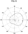
- FIG. 15 is a diagram illustrating the directivity obtained by an electromagnetic field simulation performed by setting the resonance frequency of the antenna device 100M1 to 28 GHz.
- the directivity illustrated in FIG. 15 is the directivity of the main lobe of the antenna device 100M1.
- the direction of 0 degrees corresponds to the +Z direction
- the direction of 90 degrees corresponds to the +X direction.
- FIG. 15 it can be understood that the directivity in the +Z direction (0 degree direction) is obtained.
- the directivity when the antenna device 100M1 is attached to the electronic apparatus 200 is considered to be substantially the same as the directivity when the antenna device 100 is attached to the electronic apparatus 200 as illustrated in FIG. 10 .
- the antenna device 100M1 has a configuration in which the transparent antenna element 110M1 is provided on the transparent substrate 101.
- the transparent antenna element 110M1 is provided at a position visible from the outside of the transparent cover 220, and is stacked on the display panel 231 (see FIG. 3 ).
- the antenna device 100M1 can be provided that includes a transparent antenna element 110M1 that can be provided at a position visible from the outside of the transparent cover 220 of the electronic apparatus 200, the transparent portion of the microstrip line 120M1 on the +Z direction side, and the transparent substrate 101.
- the antenna element 110M1 of the Vivaldi antenna and the microstrip line 120M1 can be formed very thin.
- the allowable thickness of the antenna device 100M1 is greatly limited, e.g., 100 ⁇ m or less, it is difficult to use an antenna device such as a patch antenna which requires a certain thickness for the ground layer.
- the antenna device 100M1 including the antenna element 110M1 of the Vivaldi antenna and the microstrip line 120M1, which can be formed very thin, is very advantageous from the viewpoint of reduction in the thickness.
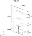
- FIGs. 16 and 17 are drawings illustrating the antenna device 100M2.
- FIGs. 16 and 17 illustrate the antenna device 100M2 in a state before being bent in parallel with the YZ plane.
- the antenna device 100M2 includes portions 100M2A and 100M2B.
- the portions 100M2A and 100M2B are similar to the portions 100A and 100B illustrated in FIGs. 1 , 2 , 4 , and 5 .
- the portion 100M2A is visible from the outside of the electronic apparatus 200 or 200A through the transparent cover 220 or 220A of the electronic apparatus 200 or 200A.
- the portion 100M2B is a portion that is situated on the rear side of the display operation unit 230 or 230A and that is not visible from the outside of the electronic apparatus 200 or 200A.
- FIGs. 16 and 17 illustrate, for example, a configuration in which the boundary between the portion 100M2A and the portion 100M2B is 1/2 from the end portion, on the +Z direction side, of the microstrip line 120 in the Z direction.
- the antenna device 100M2 includes a substrate 101, an antenna element 110, directors 115, and a microstrip line 120.
- the antenna device 100M2 is a Yagi-Uda antenna in which the directors 115 is added to the antenna device 100 illustrated in FIGs. 4 and 5 .
- the directors 115 are implemented by the transparent conductor 300A (see FIG. 6 ).
- the length in the Z direction of the microstrip line 120 having the transmission line 121 and the ground layer 122 is shorter than the length in the Z direction of the microstrip line 120 of the antenna device 100 illustrated in FIGs. 4 and 5 , but the configuration thereof is substantially the same.
- FIG. 17 (A) illustrates the substrate 101 and components provided on the surface of the substrate 101 on the +X direction side
- FIG. 17 (B) illustrates components provided on the surface of the substrate 101 on the +X direction side.
- the position of the substrate 101 is indicated by a broken line.
- the directors 115 include two directors 115A, 115B.
- the directors 115A and 115B are simply referred to as the directors 115.
- FIGs. 16 and 17 illustrate a configuration in which the directors 115 include two directors 115A and 115B, the number of directors 115 may be 1, or may be 3 or more.
- the length of the directors 115A, 115B in the Y direction is slightly shorter than the length between the open end 111C and the open end 112C of the antenna element 110.
- a gap G between the director 115A and the director 115B in the Z direction is equal to a gap G in the Z direction between: the section between the open ends 111C and 112C of the antenna element 110; and the director 115A.
- the portion 100A illustrated in FIGs. 1 and 2 .
- a portion of the antenna device 100M2 where the remaining portion of the microstrip line 120 is provided is the portion 100B illustrated in FIGs. 1 and 2 . Since the portion 100A is situated over the display panel 231 illustrated in FIG. 3 , the portion 100A may be transparent to avoid obstructing the display.
- FIG. 18 is a drawing illustrating between the relationship between the number of directors 115, the gap G, the directivity, and the gain.
- FIG. 18 (A) illustrates characteristics of directivity with respect to the gap G.
- FIG. 18 (B) illustrates the characteristics of the gain with respect to the gap G.
- the number of directors 115 is 0, 1, 3, or 5.
- the antenna element 110 is a dipole antenna, and when the number of directors 115 is 1, 3 or 5, the antenna element 110 is a Yagi-Uda antenna.
- the directivity represents an angle (deg.) of the main lobe, and the gain represents a gain (dBi) of the main lobe.
- the number of the directors 115 In the case where the number of the directors 115 was 1, when the gap G was set to 3 mm or more, a directivity of about 10 degrees was obtained. In the case where the number of the directors 115 was 3, when the gap G was set to 3 mm and 4 mm, a directivity of about 10 degrees was obtained, and when the gap was set to 5 mm or more, a directivity of about 90 degrees or more was obtained. In the case where the number of the directors 115 was 5, when the gap G was set to 3, a directivity of about 10 degrees was obtained, and when the gap G was set to 4 mm or more, a directivity of about 75 degrees or more was obtained.
- the directivity of the dipole antenna is about 35 degrees, it was found that the directivity can be adjusted by selecting the number and the number of directors 115.
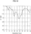
- FIG. 19 is a diagram illustrating frequency characteristics of the S11 parameter of the antenna device 100M2 in which there is only one director 115 and the gap G is set to 4 mm.
- the antenna device 100M2 in which there is only one director 115 and the gap G is set to 4 mm is configured so as to obtain the maximum gain when there is only one director 115 (see FIG. 18 (B) ).
- FIG. 19 illustrates frequency characteristics of the S11 parameter obtained by an electromagnetic field simulation performed by setting the resonance frequency of the antenna device 100M2 to 28 GHz. An adequate bandwidth in which the S11 parameter becomes -5 dB or less was obtained at around 28 GHz.
- FIG. 20 is a diagram illustrating the directivity obtained by an electromagnetic field simulation performed by setting, to 28 GHz, the resonance frequency of the antenna device 100M2 in which there is only one director 115 and the gap G is set to 4 mm.
- the directivity illustrated in FIG. 20 is the directivity of the main lobe of the antenna device 100M2.
- the direction of 0 degrees corresponds to the +Z direction
- the direction of 90 degrees corresponds to the +X direction.
- FIG. 20 it can be understood that the directivity in the +Z direction (0 degree direction) was obtained.
- the directivity in the case where the antenna device 100M2 in which there is only one director 115 and the gap G is set to 4 mm is attached to the electronic apparatus 200 is substantially the same as the directivity in the case where the antenna device 100 is attached to the electronic apparatus 200 as illustrated in FIG. 10 .
- FIG. 21 is a diagram illustrating frequency characteristics of the S11 parameter of the antenna device 100M2 of which the number of directors 115 is 5 and of which the gap G is set to 1 mm.
- the antenna device 100M2 of which the number of directors 115 is 5 and of which the gap G is set to 1 mm is configured so as to obtain the maximum gain when the number of directors 115 is 5 (see FIG. 18 (B) ).
- FIG. 21 illustrates frequency characteristics of the S11 parameter obtained by an electromagnetic field simulation performed by setting the resonance frequency of the antenna device 100M2 to 28 GHz. An adequate bandwidth in which the S11 parameter becomes -5 dB or less was obtained at around 28 GHz.
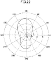
- FIG. 22 is a diagram illustrating the directivity obtained by an electromagnetic field simulation performed by setting, to 28 GHz, the resonance frequency of the antenna device 100M2 of which the number of directors 115 is 5 and of which the gap G is set to 1 mm.
- the directivity illustrated in FIG. 22 is the directivity of the main lobe of the antenna device 100M2. As illustrated in FIG. 22 , it can be understood that the directivity in the +X direction (90 degrees direction) was obtained.
- the directivity in the case where the antenna device 100M2 of which the number of directors 115 is 5 and of which the gap G is set to 1 mm is attached to the electronic apparatus 200 is a vertically upward direction with respect to the transparent cover 220 of the electronic apparatus 200.
- FIG. 23 is a drawing illustrating the directivity of the antenna device 100M2 in an exemplary cross section of the electronic apparatus 200A.
- the portion 100M2A is illustrated in white with an outline, and the portion 100M2B is illustrated in gray.
- the portion 100M2A of the antenna device 100M2 is provided over an upper surface portion 220A1 of the transparent cover 220A and a curved portion 220A2 on the -Z direction side.
- the portion 100M2A is a portion that is provided with the antenna element 110 illustrated in FIGs. 16 and 17 , the director 115, and a portion of the microstrip line 120 on the +Z direction side, and is a transparent portion.
- the portion 100M2B of the antenna device 100M2 is provided on the rear side of the display operation unit 230A.
- the portion 100M2B is a portion that is provided with the remaining portion not included in the portion 100A of the microstrip line 120 illustrated in FIGs. 16 and 17 , and is a non-transparent portion.
- the portion 100M2A of the antenna device 100M2 is illustrated between the transparent cover 220A and the display operation unit 230A for the convenience of explanation, but the portion 100M2A of the antenna device 100M2 is not limited to be provided between the display operation unit 230A and the transparent cover 220A, and may be provided between the layers 232 and 233 as illustrated in FIG. 3 , between the layer 233 and the adhesive layer 234, or between the layer 232 and the display panel 231.
- the directivity illustrated in FIG. 22 is in the direction illustrated by (2) in FIG. 23 .
- the antenna device 100M2 can radiate electromagnetic waves in the direction indicated by (2) and can receive electromagnetic waves in the direction indicated by (2).
- the direction indicated by (2) is the direction of radiation along the direction normal to the upper surface portion 220A1 of the transparent cover 220A of the electronic apparatus 200A.
- the upper surface portion 220A1 of the transparent cover 220A is a portion of the surface of the transparent cover 220A and a portion of the surface of the electronic apparatus 200A. Since the antenna device 100 has the directivity oriented in the direction (2), the antenna device 100 can communicate with a communication device external to the electronic apparatus 200.
- the antenna device 100M2 additionally includes a director 115 as compared with the antenna device 100.
- the transparent antenna element 110, the director 115, and the portion of the microstrip line 120 that is included in the portion 100M2A are provided at a position visible from the outside of the transparent cover 220, and are stacked on the display panel 231 (see FIG. 3 ).
- the antenna device 100M2 can be provided that includes the transparent antenna element 110 that can be provided at a position visible from the outside of the transparent cover 220 of the electronic apparatus 200, the transparent director 115, the transparent portion of the microstrip line 120 that is included in the portion 100M2A, and the transparent substrate 101.
- the antenna element 110, the director 115, and the microstrip line 120 can be formed very thin.
- the allowable thickness of the antenna device 100M2 is greatly limited, e.g., 100 ⁇ m or less, it is difficult to use an antenna device such as a patch antenna which requires a certain thickness for the ground layer.
- the antenna device 100M2 including the antenna element 110, the director 115, and the microstrip line 120, which can be formed very thin, is very advantageous from the viewpoint of reduction in the thickness.
- FIG. 24 is a cross-sectional view illustrating an electronic apparatus 200B according to a modified embodiment of the embodiment.
- FIG. 24 illustrates a cross section corresponding to FIG. 11 .
- the electronic apparatus 200B includes an antenna device 100 and an antenna device 100M2.
- the antenna device 100 and the antenna device 100M2 include a common substrate 101B instead of the substrate 101 illustrated in FIGs. 4 , 5 , 16 , and 17 .
- the antenna device 100 and the antenna device 100M2 may have configurations with resonance frequencies different from each other.
- the substrate 101B is larger than the display operation unit 230A in a plan view, and is provided over the entire area between the transparent cover 220A and the display operation unit 230A.
- the end portions 101B1, 101B2 of the substrate 101B are bent and situated on the rear side of the display operation unit 230A, and are connected to the circuit board 240.
- the antenna device 100 is provided on the upper surface portion 220A1 and the curved portion 220A2 on the - Z direction side.
- the antenna device 100M2 is provided on the upper surface portion 220A1 and a curved portion 220A3 on the +Z direction side. Therefore, in the portion where the antenna device 100 and the antenna device 100M2 are not provided, only the substrate 101B is provided in the Z direction between the transparent cover 220A and the display operation unit 230A.
- the reason why the substrate 101B is made larger than the display operation unit 230A in a plan view and the end portions 101B1, 101B2 of the substrate 101B are provided on the rear side of the display operation unit 230A is to prevent the end portions 101B1, 101B2 from being seen from the outside of the transparent cover 220A in consideration of the case where the end portions 101B1, 101B2 of the substrate 101B are conspicuous.
- the end portions 101B1, 101B2 may be situated on the rear side of the display operation unit 230A including the display panel 231 (see FIG. 3 ), and do not have to be connected to the circuit board 240 as illustrated in FIG. 24 .
- the end portion of the substrate 101B is bent and positioned on the rear side of the display operation unit 230A in the XY section. This is to prevent the end portions of the substrate 101B from being seen from the outside of the transparent cover 220A.
- the portion 100A of the antenna device 100 is provided over the flat upper surface portion 220A1 and the curved portion 220A2 of the transparent cover 220A.
- the range of the portion 100A is substantially the same as FIG. 11 .
- the range of the portion 100B is also substantially the same as FIG. 11 .
- the portion 100A of the antenna device 100 is illustrated between the transparent cover 220A and the display operation unit 230A for the convenience of explanation, but the portion 100A of the antenna device 100 is not limited to be provided between the display operation unit 230A and the transparent cover 220A, and may be provided between the layers 232 and 233 illustrated in FIG. 3 , between the layer 233 and the adhesive layer 234, or between the layer 232 and the display panel 231.
- the portion 100M2A of the antenna device 100M2 is provided over the curved portion 220A3 of the transparent cover 220A on the +Z direction side and the upper surface portion 220A1.
- the portion 100M2A of the antenna device 100M2 is illustrated between the transparent cover 220A and the display operation unit 230A for the convenience of explanation, but the portion 100M2A of the antenna device 100M2 is not limited to be provided between the display operation unit 230A and the transparent cover 220A, and may be provided between the layers 232 and 233 illustrated in FIG. 3 , between the layer 233 and the adhesive layer 234, or between the layer 232 and the display panel 231.
- the antenna device 100 and the antenna device 100M2 includes a substrate 101B larger than the display operation unit 230A, and has the end portions 101B1, 101B2 of the substrate 101B situated on the rear side of the display operation unit 230A.
- the configuration may be such that any one of the antenna device 100 and the antenna device 100M2 is included.
- the electronic apparatus 200B may include an antenna device other than the antenna device 100 and the antenna device 100M2, or may include 3 or more antenna devices.
- the electronic apparatus 200B includes multiple antenna devices with resonance frequencies different from each other, the electronic apparatus 200B capable of communicating in multiple communication bands can be provided.
- FIG. 25 is a drawing illustrating the antenna device 100M2.
- the antenna device 100M2 includes a substrate 101, an antenna element 110, a director 115, and a microstrip line 120.
- the antenna element 110 includes elements 111 and 112, and the microstrip line 120 has a transmission line 121 and a ground layer 122.
- FIG. 26 is a drawing for explaining a method of bending the antenna device 100M2.
- FIG. 26 (A) and (B) illustrates portions 100M2A, 100M2B, for example.
- FIG. 26 (A) illustrates an antenna device 100M2 in an unbent state
- FIG. 26 (B) illustrates an antenna device 100M2 in a bent state.
- the bending of the antenna device 100M2 is performed by using a simulation model
- the bending of the antenna device 100M2 is hereinafter explained by using a virtual jig 105 in order to allow easy understanding of the explanation.
- the model of the antenna device 100M2 includes covers 102 and 103 as illustrated in FIG. 26 (A) and (B) .
- the covers 102 and 103 are attached to the surfaces of the antenna device 100M2 on the +X direction side and the -X direction side by adhesive layers 102A and 103A, respectively.
- the size of the covers 102 and 103 is equal to the size of the substrate 101.
- the antenna device 100M2 on the side of the antenna element 110 is bent 90 degrees in the clockwise direction in FIG. 26 (B) with respect to the side of the microstrip line 120.
- the XYZ coordinates are similarly rotated by 90 degrees. That is, even after the bending, the +Z direction is the direction of the endfire of the antenna element 110.
- FIG. 27 is a diagram illustrating a bending model of the antenna device 100M2.
- FIG. 28 is a drawing illustrating the directivity of the antenna device 100M2 with different bending positions.
- the directivity of the antenna device 100M2 can be adjusted by changing the bending position.
- FIG. 29 is a drawing illustrating an antenna device 100M3 according to a modified embodiment of the embodiment.
- the antenna device 100M3 includes a substrate 101, an antenna element 110, a reflector 116, and a microstrip line 120.
- the antenna device 100M3 includes a reflector 116 instead of the director 115 of the antenna device 100M2 illustrated in FIGs. 16 and 17 . Similar to the antenna element 110, the reflector 116 is implemented by a transparent conductor 300A (see FIG. 6 ) .
- the antenna device 100M3 includes portions 100M3A and 100M3B.
- the portions 100M3A and 100M3B are substantially the same as the portions 100A and 100B illustrated in FIGs. 1 , 2 , 4 , and 5 , with the portion 100M3A being visible from the outside of the electronic apparatus 200 or 200A through the transparent cover 220 or 220A of the electronic apparatus 200 or 200A when attached to the electronic apparatus 200 or 200A, and the portion 100M3B being situated on the rear side of display operation unit 230 or 230A and being not visible from the outside of the electronic apparatus 200 or 200A.
- FIG. 29 illustrates, for example, a configuration in which the boundary between the portion 100M3A and the portion 100M3B is 1/2 from the end portion, on the +Z direction side, of the microstrip line 120 in the Z direction.
- the length of the reflector 116 in the Y direction is slightly longer than the length in the Y direction between the open end 111C and the open end 112C of the antenna element 110.
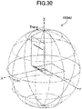
- FIG. 30 is a diagram illustrating a model of the antenna device 100M3.
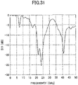
- FIG. 31 illustrates the frequency characteristics of the S11 parameter obtained by an electromagnetic field simulation performed by setting the resonance frequency of the antenna device 100M3 to 28 GHz.
- a band in which the S11 parameter becomes -5 dB or less was obtained at around 28 GHz, which is preferable.
- the directivity illustrated in FIG. 32 is the directivity of the main lobe of the antenna device 100M3.
- the direction of 0 degrees corresponds to the +Z direction (the direction of the endfire)
- the direction of 90 degrees corresponds to the +X direction
- 180 degrees corresponds to the -Z direction (the direction of the backfire).
- FIG. 32 it can be understood that a directivity in the -Z direction (backfire direction) was obtained.
- the directivity in the direction of the backfire was obtained in this manner because of the synergistic effect of the fact that the antenna device 100M3 includes the reflector 116 and the ground layer 122 is bent 90 degrees with respect to the antenna element 110 to deviate from the direction of the backfire of the antenna element 110.
- the antenna device 100M3 additionally includes the reflector 116 as compared with the antenna device 100 and is bent.
- the transparent antenna element 110 and the reflector 116 can be provided at the position visible from the outside of the transparent cover 220.
- the antenna device 100M3 can be provided that includes the transparent antenna element 110 that can be provided at a position visible from the outside of the transparent cover 220 of the electronic apparatus 200, the transparent reflector 116, the transparent portion of the microstrip line 120 on the +Z direction side, and the transparent substrate 101.
- the antenna element 110, the reflector 116, and the microstrip line 120 can be formed very thin.
- the allowable thickness of the antenna device 100M3 is greatly limited, e.g., 100 ⁇ m or less, it is difficult to use an antenna device such as a patch antenna which requires a certain thickness for the ground layer.
- the antenna device 100M3 including the antenna element 110, the reflector 116, and the microstrip line 120, which can be formed very thin, is very advantageous from the viewpoint of reduction in the thickness.
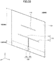
- FIG. 33 and FIG. 34 are drawings illustrating an antenna device 100M4.
- the antenna device 100M4 includes a substrate 101, an antenna element 110, a director 115, and a microstrip line 120.
- the antenna device 100M4 is a Yagi-Uda antenna, and has a configuration for a band less than 6 GHz (Sub6) of the fifth generation mobile communication system (5G).
- 5G fifth generation mobile communication system
- the antenna device 100M4 includes portions 100M4A and 100M4B.
- the portions 100M4A and 100M4B are substantially the same as the portions 100A and 100B illustrated in FIGs. 1 , 2 , 4 , and 5 , with the portion 100M4A being visible from the outside of the electronic apparatus 200 or 200A through the transparent cover 220 or 220A of the electronic apparatus 200 or 200A when attached to the electronic apparatus 200 or 200A, and the portion 100M4B being situated on the rear side of the display operation unit 230 or 230A and being not visible from the outside of the electronic apparatus 200 or 200A.
- FIG. 33 and FIG. 34 illustrate, for example, a configuration in which the boundary between the portion 100M4A and the portion 100M4B is 1/2 from the end portion, on the +Z direction side, of the microstrip line 120 in the Z direction.
- FIG. 34 (A) illustrates the substrate 101 and components provided on the surface of the substrate 101 on the +X direction side
- FIG. 34 (B) illustrates components provided on the surface of the substrate 101 on the +X direction side.
- the position of the substrate 101 is indicated by a broken line.
- the antenna device 100M4 includes, for example, one director 115.
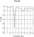
- FIG. 35 is a diagram illustrating frequency characteristics of the S11 parameter of the antenna device 100M4 including one director 115 for Sub6.
- FIG. 35 illustrates the frequency characteristics of the S11 parameter obtained by an electromagnetic field simulation performed by setting the resonance frequency of the antenna device 100M4 to 3.5 GHz. An adequate bandwidth in which the S11 parameter becomes -5 dB or less was obtained at around 3.5 GHz.
- FIG. 36 is a diagram illustrating the directivity obtained by an electromagnetic field simulation performed by setting, to 3.5 GHz, the resonance frequency of the antenna device 100M4 including one director 115 for Sub6.
- the directivity illustrated in FIG. 36 is the directivity of the main lobe of the antenna device 100M4.
- the direction of 0 degrees corresponds to the +Z direction
- the direction of 90 degrees corresponds to the +X direction.
- FIG. 36 it can be understood that the directivity in the +Z direction (0 degree direction) was obtained.
- the directivity in the case where the antenna device 100M4 including one director 115 for Sub6 is attached to the electronic apparatus 200 is substantially the same as the directivity in the case where the antenna device 100 is attached to the electronic apparatus 200 as illustrated in FIG. 10 .
- the antenna device 100M4 has a configuration in which the director 115 is added to the antenna device 100 and the size is changed for Sub6.
- the transparent antenna element 110 and the director 115 are provided at positions visible from the outside of the transparent cover 220, and are stacked on the display panel 231 (see FIG. 3 ).
- an antenna device 100M4 can be provided that includes the transparent antenna element 110 that can be provided at a position visible from the outside of the transparent cover 220 of the electronic apparatus 200, the transparent director 115, the transparent portion of the microstrip line 120 on the +Z direction side, and the transparent substrate 101.
- the antenna element 110, the reflector 115, and the microstrip line 120 can be formed very thin.
- the allowable thickness of the antenna device 100M4 is greatly limited, e.g., 100 ⁇ m or less, it is difficult to use an antenna device such as a patch antenna which requires a certain thickness for the ground layer.
- the antenna device 100M4 including the antenna element 110, the reflector 115, and the microstrip line 120, which can be formed very thin, is very advantageous from the viewpoint of reduction in the thickness.
- FIG. 37 is a drawing illustrating an electronic apparatus 200C according to a modified embodiment of the embodiment.
- the electronic apparatus 200C includes the antenna device 100M3 (see FIG. 29 ) having the directivity in the backfire direction instead of the antenna device 100 of the electronic apparatus 200A illustrated in FIG. 11 .
- the antenna device 100M3 is provided in such a manner that the bent portion of the antenna device 100M3 is situated on the rear side of the curved portion 220A2 of the transparent cover 220A on the -Z direction side, and the antenna device 100M3 can radiate electromagnetic waves in the direction indicated by (3) and can receive electromagnetic waves in the direction indicated by (3).
- the direction indicated by (3) is the direction in which radiation is emitted from the curved portion 220A2 of the transparent cover 220 of the electronic apparatus 200A toward the outside of the electronic apparatus 200A. Since the antenna device 100M3 has the directivity oriented in the direction (3), the antenna device 100M3 can communicate with a communication device external to the electronic apparatus 200A.
- the antenna device 100M3 having the directivity in the direction of the backfire is provided on the rear side of the curved portion 220A2 of the transparent cover 220A, the directivity toward the outside further away from the transparent cover 220 and the housing 210 can be obtained.
- FIG. 38 is a drawing illustrating an electronic apparatus 200D according to a modified embodiment of the embodiment.
- the electronic apparatus 200D is obtained by changing the antenna device 100M3 of the electronic apparatus 200C illustrated in FIG. 37 to the antenna device 100 illustrated in FIGs. 4 and 5 .
- the antenna device 100 has the directivity in the direction of the endfire.
- the antenna device 100 is provided so as to be gently bent between the portions 100A and 100B on the rear side of the curved portion 220A2 of the transparent cover 220A on the -Z direction side, and the antenna device 100 can radiate electromagnetic waves in the direction indicated by (4) and can receive electromagnetic waves in the direction indicated by (4).
- the direction indicated by (4) is the direction in which radiation is emitted from the upper surface portion 220A1 and the curved portion 220A2 of the transparent cover 220 of the electronic apparatus 200A toward the outside of the electronic apparatus 200A. Since the antenna device 100M3 has the directivity oriented in the direction (4), the antenna device 100M3 can communicate with a communication device external to the electronic apparatus 200A.
- the antenna device 100 having the directivity in the direction of the endfire is provided on the rear side of the curved portion 220A2 of the transparent cover 220A, the directivity toward the outside further away from the transparent cover 220 and the housing 210 can be obtained.
Landscapes
- Engineering & Computer Science (AREA)
- Computer Networks & Wireless Communication (AREA)
- Details Of Aerials (AREA)
- Support Of Aerials (AREA)
- Radar Systems Or Details Thereof (AREA)
- Control And Other Processes For Unpacking Of Materials (AREA)
- Burglar Alarm Systems (AREA)
Applications Claiming Priority (2)
| Application Number | Priority Date | Filing Date | Title |
|---|---|---|---|
| JP2020016621 | 2020-02-03 | ||
| PCT/JP2021/000849 WO2021157303A1 (ja) | 2020-02-03 | 2021-01-13 | アンテナ装置 |
Publications (2)
| Publication Number | Publication Date |
|---|---|
| EP4080680A1 true EP4080680A1 (de) | 2022-10-26 |
| EP4080680A4 EP4080680A4 (de) | 2024-01-17 |
Family
ID=77200004
Family Applications (1)
| Application Number | Title | Priority Date | Filing Date |
|---|---|---|---|
| EP21751015.5A Pending EP4080680A4 (de) | 2020-02-03 | 2021-01-13 | Antennenvorrichtung |
Country Status (6)
| Country | Link |
|---|---|
| US (1) | US12355140B2 (de) |
| EP (1) | EP4080680A4 (de) |
| JP (1) | JP7618934B2 (de) |
| KR (1) | KR102861977B1 (de) |
| CN (1) | CN114930642B (de) |
| WO (1) | WO2021157303A1 (de) |
Cited By (1)
| Publication number | Priority date | Publication date | Assignee | Title |
|---|---|---|---|---|
| US20220263224A1 (en) * | 2021-02-16 | 2022-08-18 | Dongwoo Fine-Chem Co., Ltd. | Antenna structure and image display device including the same |
Families Citing this family (4)
| Publication number | Priority date | Publication date | Assignee | Title |
|---|---|---|---|---|
| JP7415943B2 (ja) * | 2018-11-22 | 2024-01-17 | Agc株式会社 | アンテナシステム |
| TWI779339B (zh) * | 2020-08-25 | 2022-10-01 | 香港商南京矽力微電子(香港)有限公司 | 無線電子標籤及其系統 |
| KR20240130231A (ko) * | 2023-02-21 | 2024-08-29 | 삼성디스플레이 주식회사 | 안테나 모듈 및 이를 포함하는 표시 장치 |
| US20250337169A1 (en) * | 2024-04-30 | 2025-10-30 | Aptiv Technologies AG | Combined Air Waveguide Antenna and Housing |
Family Cites Families (22)
| Publication number | Priority date | Publication date | Assignee | Title |
|---|---|---|---|---|
| BE469469A (de) * | 1945-06-05 | |||
| NL251575A (de) * | 1959-05-11 | 1964-02-25 | ||
| US3438043A (en) * | 1968-07-02 | 1969-04-08 | Hermann W Ehrenspeck | Short backfire antenna |
| US3681769A (en) * | 1970-07-30 | 1972-08-01 | Itt | Dual polarized printed circuit dipole antenna array |
| US4183027A (en) * | 1977-10-07 | 1980-01-08 | Ehrenspeck Hermann W | Dual frequency band directional antenna system |
| JP2003032030A (ja) * | 2001-07-17 | 2003-01-31 | Mitsubishi Cable Ind Ltd | 漏洩導波管 |
| JP4754601B2 (ja) * | 2005-01-31 | 2011-08-24 | 富士通コンポーネント株式会社 | アンテナ装置 |
| CN104396358A (zh) * | 2012-04-18 | 2015-03-04 | 柯尼卡美能达株式会社 | 透光性导电图案部件及使用了其的透光性电磁屏蔽·天线部件 |
| JP2013254375A (ja) * | 2012-06-07 | 2013-12-19 | Fujitsu Component Ltd | タッチパネル及びその製造方法 |
| CN203366269U (zh) * | 2013-04-12 | 2013-12-25 | 深圳欧菲光科技股份有限公司 | 触控面板及触控显示装置 |
| JP2016154271A (ja) | 2013-06-21 | 2016-08-25 | 旭硝子株式会社 | アンテナ及びそれを備える無線装置 |
| US9465501B2 (en) * | 2013-09-11 | 2016-10-11 | Eastman Kodak Company | Multi-layer micro-wire substrate method |
| KR102243381B1 (ko) * | 2014-11-07 | 2021-04-22 | 삼성전자주식회사 | 안테나 장치 |
| KR20160080444A (ko) * | 2014-12-29 | 2016-07-08 | 삼성전자주식회사 | 안테나 장치 및 그를 구비하는 전자 장치 |
| EP3428769A4 (de) * | 2016-03-10 | 2019-03-13 | Kunshan Visionox Technology Co., Ltd. | Anzeigevorrichtung mit nfc-kommunikationsfunktion |
| JP2017175338A (ja) * | 2016-03-23 | 2017-09-28 | Smk株式会社 | 導電性フィルムおよびこれを備えたタッチパネル |
| JP6948607B2 (ja) * | 2016-03-25 | 2021-10-13 | 大日本印刷株式会社 | アンテナ |
| JP6768212B2 (ja) * | 2016-03-25 | 2020-10-14 | 大日本印刷株式会社 | アンテナ |
| US10775490B2 (en) * | 2017-10-12 | 2020-09-15 | Infineon Technologies Ag | Radio frequency systems integrated with displays and methods of formation thereof |
| JP7180170B2 (ja) | 2018-07-27 | 2022-11-30 | 三菱電機株式会社 | Tmrセンサの出力補正方法 |
| KR102057315B1 (ko) * | 2018-10-18 | 2019-12-18 | 주식회사 센서뷰 | 밀리미터파(mmWave) 대역용 전송선로 일체형 저손실 유연 안테나 |
| CN116111335B (zh) * | 2021-11-10 | 2025-08-26 | 财团法人工业技术研究院 | 透光天线 |
-
2021
- 2021-01-13 CN CN202180008451.8A patent/CN114930642B/zh active Active
- 2021-01-13 JP JP2021575680A patent/JP7618934B2/ja active Active
- 2021-01-13 KR KR1020227025930A patent/KR102861977B1/ko active Active
- 2021-01-13 EP EP21751015.5A patent/EP4080680A4/de active Pending
- 2021-01-13 WO PCT/JP2021/000849 patent/WO2021157303A1/ja not_active Ceased
-
2022
- 2022-07-15 US US17/812,849 patent/US12355140B2/en active Active
Cited By (2)
| Publication number | Priority date | Publication date | Assignee | Title |
|---|---|---|---|---|
| US20220263224A1 (en) * | 2021-02-16 | 2022-08-18 | Dongwoo Fine-Chem Co., Ltd. | Antenna structure and image display device including the same |
| US11804646B2 (en) * | 2021-02-16 | 2023-10-31 | Dongwoo Fine-Chem Co., Ltd. | Antenna structure and image display device including the same |
Also Published As
| Publication number | Publication date |
|---|---|
| WO2021157303A1 (ja) | 2021-08-12 |
| JPWO2021157303A1 (de) | 2021-08-12 |
| EP4080680A4 (de) | 2024-01-17 |
| CN114930642B (zh) | 2024-01-12 |
| JP7618934B2 (ja) | 2025-01-22 |
| KR102861977B1 (ko) | 2025-09-19 |
| US20220352620A1 (en) | 2022-11-03 |
| US12355140B2 (en) | 2025-07-08 |
| KR20220130142A (ko) | 2022-09-26 |
| CN114930642A (zh) | 2022-08-19 |
Similar Documents
| Publication | Publication Date | Title |
|---|---|---|
| US12355140B2 (en) | Antenna device | |
| CN113540804B (zh) | 具有带寄生贴片的电介质谐振器天线的电子设备 | |
| CN114628886B (zh) | 具有探针馈电的电介质谐振器天线的电子设备 | |
| CN111610883B (zh) | 触控显示屏及电子设备 | |
| CN115275557B (zh) | 具有折叠天线模块的电子设备 | |
| US12519217B2 (en) | Display apparatus and electronic device | |
| JP7657404B2 (ja) | 透明アンテナ及びディスプレイモジュール | |
| US20230063968A1 (en) | Transparent antenna, antenna array, and display module | |
| US11664601B2 (en) | Electronic devices with coexisting antennas | |
| CN112306299B (zh) | 集成天线的触控面板和电子设备 | |
| CN215869800U (zh) | 天线装置和包括该天线装置的显示装置 | |
| WO2022121765A1 (zh) | 显示屏模组及电子设备 | |
| CN118232026B (zh) | 一种天线结构和电子设备 | |
| CN116598780B (zh) | 具有弯曲的电介质谐振器天线的电子设备 | |
| GB2624521A (en) | Electronic devices with dielectric resonator antennas | |
| US12206189B2 (en) | Multi-layer dielectric resonator antennas with parasitic elements | |
| EP4421982A1 (de) | Antennenmodul und anzeigevorrichtung damit | |
| CN120021387A (zh) | 包括天线和天线电路板的显示装置 | |
| JP7771893B2 (ja) | アンテナ装置、及び、アンテナ付ディスプレイ装置 | |
| JP7743799B2 (ja) | アンテナ装置、及び、電子機器 | |
| WO2021161803A1 (ja) | アンテナ装置 | |
| US20250372861A1 (en) | Electronic Device with Antenna Overlapping Inactive Display Region | |
| CN116615840B (zh) | 用于电磁波的重定向结构 | |
| TW202025555A (zh) | 多天線系統及其電子裝置 | |
| CN111342242A (zh) | 多天线系统及其电子装置 |
Legal Events
| Date | Code | Title | Description |
|---|---|---|---|
| STAA | Information on the status of an ep patent application or granted ep patent |
Free format text: STATUS: THE INTERNATIONAL PUBLICATION HAS BEEN MADE |
|
| PUAI | Public reference made under article 153(3) epc to a published international application that has entered the european phase |
Free format text: ORIGINAL CODE: 0009012 |
|
| STAA | Information on the status of an ep patent application or granted ep patent |
Free format text: STATUS: REQUEST FOR EXAMINATION WAS MADE |
|
| 17P | Request for examination filed |
Effective date: 20220718 |
|
| AK | Designated contracting states |
Kind code of ref document: A1 Designated state(s): AL AT BE BG CH CY CZ DE DK EE ES FI FR GB GR HR HU IE IS IT LI LT LU LV MC MK MT NL NO PL PT RO RS SE SI SK SM TR |
|
| DAV | Request for validation of the european patent (deleted) | ||
| DAX | Request for extension of the european patent (deleted) | ||
| REG | Reference to a national code |
Ref country code: DE Ref legal event code: R079 Free format text: PREVIOUS MAIN CLASS: H01Q0001240000 Ipc: H01Q0001080000 |
|
| A4 | Supplementary search report drawn up and despatched |
Effective date: 20231218 |
|
| RIC1 | Information provided on ipc code assigned before grant |
Ipc: H01Q 19/30 20060101ALN20231212BHEP Ipc: H01Q 13/10 20060101ALN20231212BHEP Ipc: H01Q 13/08 20060101ALN20231212BHEP Ipc: H01Q 11/10 20060101ALN20231212BHEP Ipc: H01Q 9/30 20060101ALN20231212BHEP Ipc: H01Q 9/06 20060101ALN20231212BHEP Ipc: H01Q 1/36 20060101ALI20231212BHEP Ipc: H01Q 1/44 20060101ALI20231212BHEP Ipc: H01Q 1/38 20060101ALI20231212BHEP Ipc: H01Q 1/24 20060101ALI20231212BHEP Ipc: H01Q 1/08 20060101AFI20231212BHEP |
|
| STAA | Information on the status of an ep patent application or granted ep patent |
Free format text: STATUS: EXAMINATION IS IN PROGRESS |
|
| 17Q | First examination report despatched |
Effective date: 20260121 |