EP4081841B1 - Dispositif optique avec correction de phase - Google Patents
Dispositif optique avec correction de phase Download PDFInfo
- Publication number
- EP4081841B1 EP4081841B1 EP20828750.8A EP20828750A EP4081841B1 EP 4081841 B1 EP4081841 B1 EP 4081841B1 EP 20828750 A EP20828750 A EP 20828750A EP 4081841 B1 EP4081841 B1 EP 4081841B1
- Authority
- EP
- European Patent Office
- Prior art keywords
- optical element
- electromagnetic radiation
- layer
- metasurface
- phase delay
- Prior art date
- Legal status (The legal status is an assumption and is not a legal conclusion. Google has not performed a legal analysis and makes no representation as to the accuracy of the status listed.)
- Active
Links
Images


Classifications
-
- G—PHYSICS
- G02—OPTICS
- G02B—OPTICAL ELEMENTS, SYSTEMS OR APPARATUS
- G02B5/00—Optical elements other than lenses
- G02B5/18—Diffraction gratings
- G02B5/1809—Diffraction gratings with pitch less than or comparable to the wavelength
-
- G—PHYSICS
- G02—OPTICS
- G02B—OPTICAL ELEMENTS, SYSTEMS OR APPARATUS
- G02B1/00—Optical elements characterised by the material of which they are made; Optical coatings for optical elements
- G02B1/002—Optical elements characterised by the material of which they are made; Optical coatings for optical elements made of materials engineered to provide properties not available in nature, e.g. metamaterials
-
- G—PHYSICS
- G02—OPTICS
- G02B—OPTICAL ELEMENTS, SYSTEMS OR APPARATUS
- G02B27/00—Optical systems or apparatus not provided for by any of the groups G02B1/00 - G02B26/00, G02B30/00
- G02B27/42—Diffraction optics, i.e. systems including a diffractive element being designed for providing a diffractive effect
- G02B27/4272—Diffraction optics, i.e. systems including a diffractive element being designed for providing a diffractive effect having plural diffractive elements positioned sequentially along the optical path
-
- H—ELECTRICITY
- H10—SEMICONDUCTOR DEVICES; ELECTRIC SOLID-STATE DEVICES NOT OTHERWISE PROVIDED FOR
- H10F—INORGANIC SEMICONDUCTOR DEVICES SENSITIVE TO INFRARED RADIATION, LIGHT, ELECTROMAGNETIC RADIATION OF SHORTER WAVELENGTH OR CORPUSCULAR RADIATION
- H10F77/00—Constructional details of devices covered by this subclass
- H10F77/40—Optical elements or arrangements
- H10F77/413—Optical elements or arrangements directly associated or integrated with the devices, e.g. back reflectors
-
- H—ELECTRICITY
- H10—SEMICONDUCTOR DEVICES; ELECTRIC SOLID-STATE DEVICES NOT OTHERWISE PROVIDED FOR
- H10H—INORGANIC LIGHT-EMITTING SEMICONDUCTOR DEVICES HAVING POTENTIAL BARRIERS
- H10H20/00—Individual inorganic light-emitting semiconductor devices having potential barriers, e.g. light-emitting diodes [LED]
- H10H20/80—Constructional details
- H10H20/85—Packages
- H10H20/855—Optical field-shaping means, e.g. lenses
Definitions
- a problem of attempting to mass produce metasurfaces using existing technologies and materials is that they are typically limited to a phase shift or delay between 0 to ⁇ radians.
- the optical element may further comprising a plurality of said first layers; and/or a plurality of said second layers.
- a detector for detecting electromagnetic radiation comprising a photodetector; and any of the optical elements described above arranged between a source of the electromagnetic radiation and the photodetector.
- the photodetector may comprises a photodiode.
- the photodetector may comprise one or more semiconductor layers, and the first and second layer of the optical element may be integrated on, between, or under the one or more semiconductor layers.
- this disclosure provides an optical element for introducing an arbitrary phase delay from 0 to 2 ⁇ radians into incident electromagnetic radiation or portions thereof by using metasurface layer and one classical phase shift layer.
- the transmission region 104 of the first layer 101 may comprise a non-zero refractive index medium with a predetermined transmissivity for one or more wavelengths of electromagnetic radiation at which the optical element 100 is intended to operate.
- the electromagnetic radiation propagates through the non-zero refractive index medium of the transmission region 104 causing a change of wavelength and thus introducing the first phase delay relative to propagation before the optical element 100 was reached.
- the electromagnetic radiation then propagates through the metasurface of the second layer 102 that introduces the second relative phase delay.
- a further phase delay may be introduced by the metasurface of the second layer 202.
- the amount of relative phase delay introduced into each portion of electromagnetic radiation 203a-e by the first layer 201 is dependent on the thickness and refractive index of the transmission region 204a-e through which that respective portion propagated. It is envisaged in the example of Figure 2 that the transmission regions 204a-e form an integral transmission medium of material having a uniform refractive index.
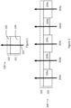
- Figure 3a shows an illustration of an exemplary optical element 300 according to an embodiment of the invention that comprises a first layer 301 and a second layer 302 such as the first and second layers described in connection with Figure 1 or 2 .
- the optical element 300 may further comprise a substrate 303 on which the first layer 301 and second layer 302 may be arranged.
- the first layer introduces respective first phase delays in the range of 0 to ⁇ radians into respective portions of incident electromagnetic radiation relative to each other based on the thicknesses and refractive index of the transmission regions through which the portions of electromagnetic radiation propagate.
- the respective first phase delays introduced by the plurality of transmission regions are dependent on the respective thicknesses of those regions.
- the second layer comprises one or more of a diffractive optical element (such as a zone plate), a mirror, a lens, or other optical element
- a phase delay will be introduced according to the known classical optical framework treatment of these optical elements.
- the second layer introduces second phase delays of an additional 0 to ⁇ radians into the respective portions of incident electromagnetic radiation relative to each other.
- the metasurface 304 of the second layer 302 comprises a plurality of structures 305 spaced apart on a surface, for example, on the upper surface of the first layer 301.
- the structures 305 have a lateral and/or vertical size smaller than a wavelength of the incident electromagnetic radiation and so are accordingly said to be sub-wavelength structures 305.
- the surface on which the structures 305 are spaced apart is arranged in respective propagation paths of respective portions of the electromagnetic radiation to introduce the respective second phase delays as described above.
- the respective second phase delays introduced by the metasurface are dependent on one or more of a: size, position of, and/or spacing between the sub-wavelength structures of the metasurface, according to predetermined metasurface design criteria as will be appreciated by the skilled person.
- the thicknesses of the plurality of transmission regions of the first layer 301 cause the respective first phase delays to be in the range of 0 to ⁇ radians
- the one or more of: the geometry of, size of, position of, and/or spacing between the structures of the metasurface of the second layer cause the respective second phase delays to be in the range of 0 to ⁇ radians, whereby the sum of the first phase delay and second phase delay introduced into each respective portion of electromagnetic radiation is in the range of 0 to 2 ⁇ radians.
- Figure 3b shows a different view of the exemplary optical element 300 illustrated in Figure 3a .
- the different transmission regions 306a-c of the first layer 301 shown in Figure 3a are also shown in Figure 3b together with further transmission regions 306d-e. It is envisaged that any transmission region configuration and thickness profile may be used as will be appreciated by the skilled person and accordingly the circular or concentric ring shapes of the transmission regions shown in Figure 3b are not intended to be limiting.
- the transmission regions 306a-e are provided under the surface on which the sub-wavelength structures 305 (not all of which are shown) are arranged.
- any sub-wavelength structure number, pattern and arrangement may be used to achieve the phase delays needed as will be appreciated by the skilled person.
- the specific size, shape, pattern and arrangement of sub-wavelength structures 306a-e illustrated in Figures 3a and 3b is not intended to be limiting.
- structures with hexagonal, rectangular, triangular, and/or any other shaped section are also envisaged to be used as will be appreciated by the skilled person.
- the phase delay introduced into respective portions of the electromagnetic radiation is in bijection correspondence with the geometric characteristics of the sub-wavelength structures.
- every pillar diameter may correspond to a unique phase delay for a unique portion of electromagnetic radiation and vice-versa where pillar height and spacing is kept constant.
- the structures are placed on a surface such as on the first layer described above (or on a substrate if the optical element is oriented the other way around) in a fashion such that every chosen pillar position causes the corresponding portion of electromagnetic radiation propagating through it to interfere constructively at one or more given points along the propagation path.
- the optical element must be able cause a phase delay of at least up to the full range of 0-2 ⁇ radians.
- a problem with known metasurfaces is that, depending on the material availability, material compatibility and/or process technologies used, phase delays of more than ⁇ and up to 2 ⁇ radian are not possible if high transmissivity is to be retained and known III-V materials mass-production techniques are to remain compatible. Accordingly, where the interference pattern requires the capability to introduce phase delays into some portions of the electromagnetic radiation that are higher than what can be achieved with the metasurface alone, the additional phase delay may be added by the classical phase delay layer described herein.
- the optical element of the present disclosure provides a phase delay layer, integrated with a metasurface, which can introduce additional phase delays as needed to achieve any arbitrary phase delay in the range of 0 to 2 ⁇ radians and thereby achieve any interference pattern at one or more predetermined distances from the optical element.
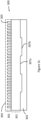
- Figure 3c shows an illustration of an optical element 300, which is the same as the optical element 300 of Figures 3a-b but wherein the thickness profile of the first layer 301 is the geometrical complement of the thickness profile of the first layer 301 of Figures 3a-b .
- the first layer 301 of Figures 3a-b has a thicker transmission region that sits in a trench in a substrate
- the corresponding transmission region 307a in Figure 3c is thinner.
- the corresponding transmission region 307b in Figure 3c is thicker and sits in a corresponding trench in the substrate.
- Figure 3c illustrates that the thicknesses of the first layer may be designed according to any required thickness profile in order to introduce any arbitrary phase delay into incident electromagnetic radiation.
- the desired phase delay layer thickness profile i.e. which transmissions regions have which thicknesses
- refractive index i.e. which transmissions regions have which thicknesses
- the design and arrangement of the sub-wavelength structures of the metasurface will be calculated using known models and algorithms. Accordingly, once the design has been chosen, the optical element may be manufactured to that design to achieve the desired interference pattern. The interference pattern produced by the optical element cannot then be changed post manufacture. Accordingly, each transmission region and the metasurface sub-wavelength structures may be said to introduce a constant phase delay into any portion of light propagating through it.
- the phase delay layer may be deposited (e.g. dielectric or amorphous silicon deposition) or epitaxially grown (e.g. indium gallium phosphide) so as to provide an etch-stop layer during etching for precise thickness control.
- the substrate material is gallium arsenide
- indium gallium phosphide provides strong edge selectivity and an efficient stopgap.
- the portions 406a-c of electromagnetic radiation then propagate through the metasurface 404 of the second layer 402 and out of the optical element 400.
- the portions of electromagnetic radiation interfere to produce the predetermined interference pattern according to the design criteria of the optical element 400 as described above, for example by constructively interfering at a focal point 409 or plane like a lens.
- the thickness(es) of the first layer is arranged to have a thickness to provide the additional phase delay that the metasurface 404 is not able to provide alone.
- the desired interference pattern requires a phase delay in the range of [0, ⁇ ] radians in one portion 406b of the electromagnetic radiation but a phase delay in the range of [ ⁇ , 2 ⁇ ] radians in the other portions 406a, 406c.
- the transmission region 407b corresponding to the portion of electromagnetic radiation which only needs a phase delay in the range of [0, ⁇ ] radians does not need to introduce an additional phase delay because the metasurface alone is capable of introducing a phase delay in this range.
- the thickness of this transmission region 407b is accordingly arranged not to introduce any additional phase delay (for example, it may have a zero thickness).
- the transmission regions 407a, 407c corresponding to the portion of electromagnetic radiation which need a phase delay in the range of [ ⁇ , 2 ⁇ ] radians do need an additional phase delay because the metasurface 404 alone can only introduce a phase delay of up to [0, ⁇ ] radians.
- the thicknesses of these transmission regions 407a, 407c are arranged to introduce an additional phase delay in the range of an additional [0, ⁇ ] radians such that the total phase delay introduced by the metasurface 404 plus the transmission regions is in the desired range of [ ⁇ , 2 ⁇ ] radians. In this way, the desired interference pattern which requires various phase delays in the range of [0, 2 ⁇ ] radians can be produced.
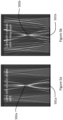
- Figure 5a shows the results of a simulation of an optical element 501a, in this case a metalens, designed to produce a predetermined interference pattern with a focal region 502a requiring phase shifts up to the full 2 ⁇ radians range using a theoretical metasurface capable of introducing the required 2 ⁇ radian phase delays.
- Mass producing the theoretical metasurface of Figure 5a using known mass production techniques is not possible for the reasons described above and the simulation is provided for illustrative purposes only.
- Figure 5b comparatively shows the results of a simulation of an optical element 501b according to the present disclosure, for example as described in connection with Figures 1-4 , designed to produce the same interference pattern as the hypothetical metasurface of Figure 5a .
- the optical element comprises a metasurface able to introduce a phase shift in the range of 0 to ⁇ radians integrated with a phase delay layer to introduce an additional phase delay of in the range of 0 to ⁇ .
- Figure 5b illustrates that the optical element 501b according to the present disclosure produces an almost identical interference pattern with a focal region 502b in approximately the same position as the hypothetical optical element 501a of Figure 5a .
- the optical element 501b of Figure 5b may be mass produced using existing mass production techniques, thereby providing a route to cheap, efficient, and quick industrialisation of metasurface technologies in a wider variety of applications than is presently viable.
- the dimensions of the metasurface structures will depend on the selected wavelength of the incident electromagnetic radiation.
- approximate structure heights may typically be in the range of 200 - 1000 nm
- approximate spacing between structure may typically be in the range of 50nm-700nm
- approximate structure diameter may typically be in the range of 50-500nm.
- the thickness values will depend not only on the wavelength but also in the requirements of the interference pattern desired, for example to create the effect of a lens, and/or on the requirements of the metasurface.
- one or more transmission regions of the delay layer may have an approximate thickness ranging from around 40nm to around 400nm with widths of one or more transmission regions being around 200nm up to the size of the of whole metasurface, for example around 50um-3mm.
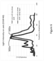
- Figure 6 shows a graph of the results of the simulations of Figures 5a and 5b whereby an electromagnetic radiation intensity value in arbitrary units is plotted against distance from the optical element 501a, 501b in micrometres.
- the graph of Figure 6 illustrates the similarity between the interference pattern produced by the optical element 501b of Figure 5b and the hypothetical optical element 501a of Figure 5a .
- the graph of Figure 6 illustrates that constructive interference that produces the respective focal regions 502a, 502b in Figures 5a and 5b occurs at approximately the same distance from the respective optical elements 501a, 501b.
- optical elements described above with reference to Figures 1-6 are said to comprise a single first layer and second layer, it is envisaged that a plurality of first layers and/or second layers may be arranged on top and/or interleaved with of each other to further customise and control the produced interference pattern.
- the optical element of the present disclosure may comprise a plurality of said first layers, and/or a plurality of said second layers.
- Figure 7 shows an illustration of an exemplary optical element 700, for example, similar to the optical elements described in connection with of Figures 1-6 .
- the optical element 700 comprises a first layer 701 comprising a plurality of transmission regions of non-zero refractive index material and having varying thicknesses, a second layer 702 comprising a metasurface 704 comprising a plurality of sub-wavelength structures 705 arranged on a surface.
- the first and second layers 701, 702 may optionally be provided on a substrate 703 made of for example gallium arsenide, or for example an epitaxy material.
- one or more intermediate layers (not shown) in or on the substrate may comprise a semiconductor light-emitting device (such as a VCSEL, LED, and/or resonant cavity LED) to provide a source for the electromagnetic radiation incident on the first and second layers.
- the substrate may also be provided with one or more transparent layers and/or reflection layers on an emission side or reverse side.
- the propagation axis of the electromagnetic radiation 706 generated by the envisaged light-emitting device is normal to the upper and lower surfaces of the optical element 700.
- an optional encapsulation material layer 707 to provide physical protection.
- this layer is transparent.
- the encapsulation material layer 707 may comprise a metal material to enhance reflectivity.
- the first layer comprises multiple layers: the plurality of transmission regions and an optional intermediate layer 708 suitable for being planarized and/or chemical-mechanically polished (for example to provide a suitable surface on which to manufacture the metasurface during mass-production without damaging the underlying phase delay layer).
- the intermediate layer may also have a predetermined reflection and/or transmission coefficient to help with the tuning of reflection and/or transmission within the optical element.
- the optical element of the present disclosure has generally been described herein to produce an interference pattern corresponding to a lens or metalens such that the optical element may be said to be a lens or metalens, it is also envisaged that the optical element may produce an interference pattern of one or more of a diffractive optical element, a diffractive optical element comprising a metalens, a mirror, a mirror comprising a metalens, and/or an optical filter.
- optical element of the present disclosure described above in connection with all of the Figures may be integrated with one or more of such optical components during manufacture thereby further enhancing the advantage that the optical element of the present disclosure provides a cheap, efficient, and quick way to industrialise metasurface technologies using existing mass-production fabrication techniques.
- a lens or metalens may be made with the one or more first and second layers described herein.
- a diffractive optical element may be made with the one or more first and second layers described herein and/or may be further integrated with a metalens made with the one or more first and second layers described herein.
- a mirror may be made with the first and second layers described herein and/or may be further integrated with a metalens made with the one or more first and second layers described herein.
- optical element of the present disclosure may be integrated into or with other types of optical components such as energy sources and detectors.
- FIG 8 shows an illustration of an exemplary energy source 800.
- the energy source is arranged to emit electromagnetic radiation 802 and comprises a light source, for example, one or more of a vertical cavity surface-emitting laser (VCSEL), a light emitting diode (LED), a resonant cavity LED, or a surface emitting laser.
- the energy source 800 further comprises an optical element 801, for example, an optical element described above in connection with all of the Figures.
- the energy source may comprise one or more semiconductor layers whereby the first and second layers of the optical element 801 are integrated on, between or under the one or more semiconductor layers such that the optical element 801 may be said to be integrated into the light source.
- Figure 9 shows an illustration of an exemplary detector 900 for detecting electromagnetic radiation 902.
- the detector 900 comprises a photodetector, for example a photodiode.
- the detector 900 further comprises an optical element 901, for example, an optical element described above in connection with all of the Figures.
- the detector 900 may comprise one or more semiconductor layers whereby the first and second layers of the optical element 901 are integrated on, between or under the one or more semiconductor layers such that the optical element 901 may be said to be integrated into the detector.
- Embodiments of the present disclosure can be employed in many different applications including, for example, in structured light, integrated optics, lens on VCSEL metalens, and/or LIDAR applications.
Landscapes
- Physics & Mathematics (AREA)
- General Physics & Mathematics (AREA)
- Optics & Photonics (AREA)
- Diffracting Gratings Or Hologram Optical Elements (AREA)
- Optical Elements Other Than Lenses (AREA)
- Optical Filters (AREA)
- Semiconductor Lasers (AREA)
- Light Receiving Elements (AREA)
Claims (13)
- Élément optique (200, 300, 400, 700, 800, 900) pour introduire un retard de phase prédéterminé dans un rayonnement électromagnétique incident (203a-e, 403a-c), l'élément optique (200, 300, 400, 700, 800, 900) comprenant :une première couche (201, 301, 401, 701) et une seconde couche (202, 302, 402, 702) agencées dans un trajet de propagation d'une partie de rayonnement électromagnétique (203a-e, 403a-c, 706),la première couche (201, 302, 402, 702) étant configurée pour introduire un premier retard de phase dans la partie de rayonnement électromagnétique (203a-e, 403a-c, 706) se propageant à travers elle ;la seconde couche (202, 302, 402, 702) comprenant une métasurface (304, 404, 704) configurée pour introduire un second retard de phase dans la partie de rayonnement électromagnétique (203a-e, 403a-c, 706) se propageant à travers elle ; etla première couche (201, 301, 401, 701) comprenant :une pluralité de régions de transmission (204a-e, 306a-e, 307a-b, 407,a-c) ayant des épaisseurs respectives et agencées dans des trajets de propagation respectifs des parties respectives du rayonnement magnétique électromagnétique (203a-e, 403a-c, 706) pour introduire des premiers retards de phase respectifs dans lesdites parties respectives,caractérisé en ce que des extensions latérales respectives des régions de transmission (204a-e, 306a-e, 307a-b, 407a-c) sont supérieures à une longueur d'onde de la partie respective du rayonnement électromagnétique incident (203a-e, 403a-c, 706) se propageant à travers elles.
- Élément optique selon la revendication 1, la métasurface comprenant :une pluralité de structures (305, 405, 705) espacées sur une surface, les structures (305, 405, 705) ayant une taille latérale et/ou verticale inférieure à une longueur d'onde du rayonnement électromagnétique incident (203a-e, 403a-c, 706)et la surface étant agencée dans des trajets de propagation respectifs de parties respectives du rayonnement électromagnétique (203a-e, 403a-c, 706) pour introduire des seconds retards de phase respectifs dans lesdites parties respectives.
- Élément optique selon la revendication 2, configuré de sorte queles premiers retards de phase respectifs introduits par la pluralité de régions de transmission dépendent des épaisseurs respectives des régions de transmission ; etles seconds retards de phase respectifs introduits par la métasurface dépendent d'un ou de plusieurs des éléments suivants : géométrie, taille, position et/ou espacement entre les structures sur la surface.
- Élément optique selon les revendications 2 ou 3, configuré de sorte que, à une ou plusieurs distances prédéterminées de l'élément optique, la combinaison des premiers et seconds retards de phase respectifs amènent lesdites parties de rayonnement électromagnétique à interférer de manière constructive.
- Élément optique selon l'une quelconque des revendications 2 à 4, configuré de sorte queles épaisseurs de la pluralité de régions de transmission de la première couche amènent les premiers retards de phase respectifs à être dans la plage de 0 à π radians,le ou les des éléments suivants : la géométrie, la taille, la position et/ou l'espacement entre les structures de la métasurface de la seconde couche amènent les seconds retards de phase respectifs à être dans la plage de 0 à π radians,la somme du premier retard de phase et du second retard de phase introduits dans chaque partie respective du rayonnement électromagnétique étant dans la plage de 0 à 2n radians.
- Élément optique selon n'importe quelle revendication précédente, comprenant :une pluralité desdites premières couches ; et/ouune pluralité desdites secondes couches.
- Élément optique selon n'importe quelle revendication précédente, l'élément optique étant un ou plusieurs des éléments suivants : une lentille, une méta-lentille, un élément optique diffractif et/ou un filtre optique.
- Source d'énergie (800) agencée pour émettre un rayonnement électromagnétique, la source d'énergie (800) comprenant :une source de lumière ; etl'élément optique (801) selon n'importe quelle revendication précédente agencé dans un trajet de propagation du rayonnement électromagnétique émis.
- Source d'énergie selon la revendication 8,
la source de lumière comprenant un ou plusieurs des éléments suivants : un laser à cavité verticale émettant par la surface (VCSEL), une diode électroluminescente (DEL), une DEL à cavité résonnante, ou un laser émettant par la surface. - Source d'énergie selon la revendication 8 ou 9,la source d'énergie comprenant une ou plusieurs couches semi-conductrices, etles première et seconde couches de l'élément optique étant intégrées sur, entre ou sous la ou les couches semi-conductrices.
- Détecteur (900) pour détecter un rayonnement électromagnétique, le détecteur comprenant :un photodétecteur ; etl'élément optique (901) selon n'importe quelle revendication précédente agencé entre une source du rayonnement électromagnétique et le photodétecteur.
- Détecteur selon la revendication 11,
le photodétecteur comprenant une photodiode. - Détecteur selon la revendication 11 ou 12,le photodétecteur comprenant une ou plusieurs couches semi-conductrices, etles première et seconde couches de l'élément optique étant intégrées sur, entre ou sous la ou les couches semi-conductrices.
Applications Claiming Priority (2)
| Application Number | Priority Date | Filing Date | Title |
|---|---|---|---|
| US201962952544P | 2019-12-23 | 2019-12-23 | |
| PCT/EP2020/086521 WO2021130085A1 (fr) | 2019-12-23 | 2020-12-16 | Dispositif optique avec correction de phase |
Publications (2)
| Publication Number | Publication Date |
|---|---|
| EP4081841A1 EP4081841A1 (fr) | 2022-11-02 |
| EP4081841B1 true EP4081841B1 (fr) | 2024-12-04 |
Family
ID=74141463
Family Applications (1)
| Application Number | Title | Priority Date | Filing Date |
|---|---|---|---|
| EP20828750.8A Active EP4081841B1 (fr) | 2019-12-23 | 2020-12-16 | Dispositif optique avec correction de phase |
Country Status (5)
| Country | Link |
|---|---|
| US (1) | US12607775B2 (fr) |
| EP (1) | EP4081841B1 (fr) |
| JP (1) | JP2023508378A (fr) |
| CN (1) | CN114930202A (fr) |
| WO (1) | WO2021130085A1 (fr) |
Families Citing this family (8)
| Publication number | Priority date | Publication date | Assignee | Title |
|---|---|---|---|---|
| CN119781177A (zh) | 2017-08-31 | 2025-04-08 | 梅特兰兹股份有限公司 | 透射型超表面透镜集成 |
| SG11202013228XA (en) | 2018-07-02 | 2021-01-28 | Metalenz Inc | Metasurfaces for laser speckle reduction |
| KR20220035971A (ko) | 2019-07-26 | 2022-03-22 | 메탈렌츠 인코포레이티드 | 개구-메타 표면 및 하이브리드 굴절-메타 표면 이미징 시스템 |
| CN120188073A (zh) | 2022-03-31 | 2025-06-20 | 梅特兰兹股份有限公司 | 偏振分选超颖表面微透镜阵列设备 |
| WO2025158987A1 (fr) * | 2024-01-24 | 2025-07-31 | パナソニックIpマネジメント株式会社 | Élément optique |
| WO2025158986A1 (fr) * | 2024-01-24 | 2025-07-31 | パナソニックIpマネジメント株式会社 | Élément optique |
| WO2026058609A1 (fr) * | 2024-09-12 | 2026-03-19 | ソニーセミコンダクタソリューションズ株式会社 | Partie de commande de lumière, appareil de montage de semi-conducteur et procédé de production pour un appareil de montage de semi-conducteur |
| WO2026075547A1 (fr) * | 2024-10-04 | 2026-04-09 | 삼성전자 주식회사 | Caméra comprenant une méta-lentille, et dispositif électronique pouvant être porté la comprenant |
Family Cites Families (13)
| Publication number | Priority date | Publication date | Assignee | Title |
|---|---|---|---|---|
| US3763372A (en) * | 1967-07-13 | 1973-10-02 | Inventors & Investors Inc | Zone plate optics monolithically integrated with photoelectric elements |
| WO2001065305A1 (fr) * | 2000-03-01 | 2001-09-07 | Kan Cheng | Plaque a zone de fresnel a couches multiples de zones de decalage |
| WO2006102275A2 (fr) | 2005-03-21 | 2006-09-28 | University Of Florida Research Foundation, Inc. | Structures de sous-longueurs d'ondes multicouche permettant de conferer un temps de propagation de phase controlable |
| CN100573230C (zh) | 2007-10-17 | 2009-12-23 | 中国科学院光电技术研究所 | 一种三维亚波长金属结构透镜 |
| US9971078B2 (en) | 2013-03-05 | 2018-05-15 | Rambus Inc. | Phase gratings with odd symmetry for high-resolution lensless optical sensing |
| US9482796B2 (en) * | 2014-02-04 | 2016-11-01 | California Institute Of Technology | Controllable planar optical focusing system |
| EP3112924B1 (fr) | 2015-06-30 | 2021-07-28 | ams AG | Lentille hybride optique et procédé de fabrication d'une lentille hybride optique |
| CN111065886B (zh) | 2017-07-18 | 2022-05-06 | ams传感器新加坡私人有限公司 | 生成结构光 |
| KR102486389B1 (ko) * | 2017-08-14 | 2023-01-09 | 삼성전자주식회사 | 나노구조 광학소자, 깊이 센서 및 전자장치 |
| CN119781177A (zh) * | 2017-08-31 | 2025-04-08 | 梅特兰兹股份有限公司 | 透射型超表面透镜集成 |
| US11016227B2 (en) | 2017-09-18 | 2021-05-25 | Lumentum Operations Llc | Diffractive optical element |
| US11222987B2 (en) * | 2018-03-21 | 2022-01-11 | Intel Corporation | Optical receiver employing a metasurface collection lens having concentric belts or rings |
| WO2025122493A1 (fr) * | 2023-12-04 | 2025-06-12 | Lightwave Logic, Inc. | Chromophores optiques non linéaires contenant des groupes de pontage spirofluorène-isophorone, et leurs procédés de fabrication et d'utilisation |
-
2020
- 2020-12-16 CN CN202080089767.XA patent/CN114930202A/zh active Pending
- 2020-12-16 EP EP20828750.8A patent/EP4081841B1/fr active Active
- 2020-12-16 WO PCT/EP2020/086521 patent/WO2021130085A1/fr not_active Ceased
- 2020-12-16 US US17/787,742 patent/US12607775B2/en active Active
- 2020-12-16 JP JP2022538863A patent/JP2023508378A/ja active Pending
Also Published As
| Publication number | Publication date |
|---|---|
| JP2023508378A (ja) | 2023-03-02 |
| CN114930202A (zh) | 2022-08-19 |
| US12607775B2 (en) | 2026-04-21 |
| EP4081841A1 (fr) | 2022-11-02 |
| WO2021130085A1 (fr) | 2021-07-01 |
| US20230088107A1 (en) | 2023-03-23 |
Similar Documents
| Publication | Publication Date | Title |
|---|---|---|
| EP4081841B1 (fr) | Dispositif optique avec correction de phase | |
| US11762134B2 (en) | Diffractive optical element | |
| US20090097522A1 (en) | Vertical cavity surface emitting laser device | |
| KR102420016B1 (ko) | 반사층을 가지는 광변조기 | |
| KR102158054B1 (ko) | 경조 격자 렌즈를 포함하는 광학 장치 | |
| Wu et al. | Sub-wavelength GaN-based membrane high contrast grating reflectors | |
| US20210167580A1 (en) | Top emitting vcsel array with integrated gratings | |
| CN110221447A (zh) | 一种基于超构表面的结构光投影衍射光学器件 | |
| JPH07198907A (ja) | 光素子およびその製造方法 | |
| US20190363513A1 (en) | Monolithically integrated laser with led pump | |
| WO2017175148A1 (fr) | Source de lumière hautement directionnelle à rendement d'extraction élevé, et procédé de fabrication de cette source de lumière | |
| CN105164871A (zh) | 模式控制激光系统 | |
| CN102170092A (zh) | 一种偏振稳定的垂直腔面发射激光器及其制作方法 | |
| US8228604B2 (en) | Electromagnetic (EM) wave polarizing structure and method for providing polarized electromagnetic (EM) wave | |
| US20250286349A1 (en) | Vertical-cavity surface-emitting laser with integrated multi-layer meta-surface with suppressed back reflections | |
| CN1206643C (zh) | 光学构件和使用该光学构件的光学装置 | |
| JP7328582B2 (ja) | モノリシックミラーの作製方法 | |
| US6574249B2 (en) | Thin film laser emitting device and method for the manufacture thereof | |
| JP5217100B2 (ja) | 光学ユニット | |
| CN107703624B (zh) | 基于非周期亚波长光栅和分布布拉格反射镜的谐振腔 | |
| JP2013231779A (ja) | 反射防止構造及び光学部材 |
Legal Events
| Date | Code | Title | Description |
|---|---|---|---|
| STAA | Information on the status of an ep patent application or granted ep patent |
Free format text: STATUS: UNKNOWN |
|
| STAA | Information on the status of an ep patent application or granted ep patent |
Free format text: STATUS: THE INTERNATIONAL PUBLICATION HAS BEEN MADE |
|
| PUAI | Public reference made under article 153(3) epc to a published international application that has entered the european phase |
Free format text: ORIGINAL CODE: 0009012 |
|
| STAA | Information on the status of an ep patent application or granted ep patent |
Free format text: STATUS: REQUEST FOR EXAMINATION WAS MADE |
|
| 17P | Request for examination filed |
Effective date: 20220725 |
|
| AK | Designated contracting states |
Kind code of ref document: A1 Designated state(s): AL AT BE BG CH CY CZ DE DK EE ES FI FR GB GR HR HU IE IS IT LI LT LU LV MC MK MT NL NO PL PT RO RS SE SI SK SM TR |
|
| DAV | Request for validation of the european patent (deleted) | ||
| DAX | Request for extension of the european patent (deleted) | ||
| P01 | Opt-out of the competence of the unified patent court (upc) registered |
Effective date: 20230724 |
|
| GRAP | Despatch of communication of intention to grant a patent |
Free format text: ORIGINAL CODE: EPIDOSNIGR1 |
|
| STAA | Information on the status of an ep patent application or granted ep patent |
Free format text: STATUS: GRANT OF PATENT IS INTENDED |
|
| INTG | Intention to grant announced |
Effective date: 20240801 |
|
| GRAS | Grant fee paid |
Free format text: ORIGINAL CODE: EPIDOSNIGR3 |
|
| GRAA | (expected) grant |
Free format text: ORIGINAL CODE: 0009210 |
|
| STAA | Information on the status of an ep patent application or granted ep patent |
Free format text: STATUS: THE PATENT HAS BEEN GRANTED |
|
| AK | Designated contracting states |
Kind code of ref document: B1 Designated state(s): AL AT BE BG CH CY CZ DE DK EE ES FI FR GB GR HR HU IE IS IT LI LT LU LV MC MK MT NL NO PL PT RO RS SE SI SK SM TR |
|
| REG | Reference to a national code |
Ref country code: CH Ref legal event code: EP |
|
| REG | Reference to a national code |
Ref country code: DE Ref legal event code: R096 Ref document number: 602020042656 Country of ref document: DE |
|
| REG | Reference to a national code |
Ref country code: IE Ref legal event code: FG4D |
|
| REG | Reference to a national code |
Ref country code: LT Ref legal event code: MG9D |
|
| REG | Reference to a national code |
Ref country code: NL Ref legal event code: MP Effective date: 20241204 |
|
| PG25 | Lapsed in a contracting state [announced via postgrant information from national office to epo] |
Ref country code: HR Free format text: LAPSE BECAUSE OF FAILURE TO SUBMIT A TRANSLATION OF THE DESCRIPTION OR TO PAY THE FEE WITHIN THE PRESCRIBED TIME-LIMIT Effective date: 20241204 |
|
| PG25 | Lapsed in a contracting state [announced via postgrant information from national office to epo] |
Ref country code: FI Free format text: LAPSE BECAUSE OF FAILURE TO SUBMIT A TRANSLATION OF THE DESCRIPTION OR TO PAY THE FEE WITHIN THE PRESCRIBED TIME-LIMIT Effective date: 20241204 |
|
| PG25 | Lapsed in a contracting state [announced via postgrant information from national office to epo] |
Ref country code: BG Free format text: LAPSE BECAUSE OF FAILURE TO SUBMIT A TRANSLATION OF THE DESCRIPTION OR TO PAY THE FEE WITHIN THE PRESCRIBED TIME-LIMIT Effective date: 20241204 |
|
| PG25 | Lapsed in a contracting state [announced via postgrant information from national office to epo] |
Ref country code: ES Free format text: LAPSE BECAUSE OF FAILURE TO SUBMIT A TRANSLATION OF THE DESCRIPTION OR TO PAY THE FEE WITHIN THE PRESCRIBED TIME-LIMIT Effective date: 20241204 |
|
| PG25 | Lapsed in a contracting state [announced via postgrant information from national office to epo] |
Ref country code: NO Free format text: LAPSE BECAUSE OF FAILURE TO SUBMIT A TRANSLATION OF THE DESCRIPTION OR TO PAY THE FEE WITHIN THE PRESCRIBED TIME-LIMIT Effective date: 20250304 |
|
| PG25 | Lapsed in a contracting state [announced via postgrant information from national office to epo] |
Ref country code: LV Free format text: LAPSE BECAUSE OF FAILURE TO SUBMIT A TRANSLATION OF THE DESCRIPTION OR TO PAY THE FEE WITHIN THE PRESCRIBED TIME-LIMIT Effective date: 20241204 Ref country code: GR Free format text: LAPSE BECAUSE OF FAILURE TO SUBMIT A TRANSLATION OF THE DESCRIPTION OR TO PAY THE FEE WITHIN THE PRESCRIBED TIME-LIMIT Effective date: 20250305 |
|
| PG25 | Lapsed in a contracting state [announced via postgrant information from national office to epo] |
Ref country code: RS Free format text: LAPSE BECAUSE OF FAILURE TO SUBMIT A TRANSLATION OF THE DESCRIPTION OR TO PAY THE FEE WITHIN THE PRESCRIBED TIME-LIMIT Effective date: 20250304 |
|
| PG25 | Lapsed in a contracting state [announced via postgrant information from national office to epo] |
Ref country code: NL Free format text: LAPSE BECAUSE OF FAILURE TO SUBMIT A TRANSLATION OF THE DESCRIPTION OR TO PAY THE FEE WITHIN THE PRESCRIBED TIME-LIMIT Effective date: 20241204 |
|
| REG | Reference to a national code |
Ref country code: AT Ref legal event code: MK05 Ref document number: 1748744 Country of ref document: AT Kind code of ref document: T Effective date: 20241204 |
|
| PG25 | Lapsed in a contracting state [announced via postgrant information from national office to epo] |
Ref country code: SM Free format text: LAPSE BECAUSE OF FAILURE TO SUBMIT A TRANSLATION OF THE DESCRIPTION OR TO PAY THE FEE WITHIN THE PRESCRIBED TIME-LIMIT Effective date: 20241204 |
|
| PG25 | Lapsed in a contracting state [announced via postgrant information from national office to epo] |
Ref country code: PL Free format text: LAPSE BECAUSE OF FAILURE TO SUBMIT A TRANSLATION OF THE DESCRIPTION OR TO PAY THE FEE WITHIN THE PRESCRIBED TIME-LIMIT Effective date: 20241204 |
|
| PG25 | Lapsed in a contracting state [announced via postgrant information from national office to epo] |
Ref country code: IS Free format text: LAPSE BECAUSE OF FAILURE TO SUBMIT A TRANSLATION OF THE DESCRIPTION OR TO PAY THE FEE WITHIN THE PRESCRIBED TIME-LIMIT Effective date: 20250404 |
|
| PG25 | Lapsed in a contracting state [announced via postgrant information from national office to epo] |
Ref country code: PT Free format text: LAPSE BECAUSE OF FAILURE TO SUBMIT A TRANSLATION OF THE DESCRIPTION OR TO PAY THE FEE WITHIN THE PRESCRIBED TIME-LIMIT Effective date: 20250404 |
|
| PG25 | Lapsed in a contracting state [announced via postgrant information from national office to epo] |
Ref country code: EE Free format text: LAPSE BECAUSE OF FAILURE TO SUBMIT A TRANSLATION OF THE DESCRIPTION OR TO PAY THE FEE WITHIN THE PRESCRIBED TIME-LIMIT Effective date: 20241204 |
|
| PG25 | Lapsed in a contracting state [announced via postgrant information from national office to epo] |
Ref country code: AT Free format text: LAPSE BECAUSE OF FAILURE TO SUBMIT A TRANSLATION OF THE DESCRIPTION OR TO PAY THE FEE WITHIN THE PRESCRIBED TIME-LIMIT Effective date: 20241204 Ref country code: RO Free format text: LAPSE BECAUSE OF FAILURE TO SUBMIT A TRANSLATION OF THE DESCRIPTION OR TO PAY THE FEE WITHIN THE PRESCRIBED TIME-LIMIT Effective date: 20241204 |
|
| PG25 | Lapsed in a contracting state [announced via postgrant information from national office to epo] |
Ref country code: SK Free format text: LAPSE BECAUSE OF FAILURE TO SUBMIT A TRANSLATION OF THE DESCRIPTION OR TO PAY THE FEE WITHIN THE PRESCRIBED TIME-LIMIT Effective date: 20241204 |
|
| PG25 | Lapsed in a contracting state [announced via postgrant information from national office to epo] |
Ref country code: CZ Free format text: LAPSE BECAUSE OF FAILURE TO SUBMIT A TRANSLATION OF THE DESCRIPTION OR TO PAY THE FEE WITHIN THE PRESCRIBED TIME-LIMIT Effective date: 20241204 |
|
| PG25 | Lapsed in a contracting state [announced via postgrant information from national office to epo] |
Ref country code: IT Free format text: LAPSE BECAUSE OF FAILURE TO SUBMIT A TRANSLATION OF THE DESCRIPTION OR TO PAY THE FEE WITHIN THE PRESCRIBED TIME-LIMIT Effective date: 20241204 |
|
| REG | Reference to a national code |
Ref country code: CH Ref legal event code: PL |
|
| PG25 | Lapsed in a contracting state [announced via postgrant information from national office to epo] |
Ref country code: LU Free format text: LAPSE BECAUSE OF NON-PAYMENT OF DUE FEES Effective date: 20241216 |
|
| REG | Reference to a national code |
Ref country code: DE Ref legal event code: R097 Ref document number: 602020042656 Country of ref document: DE |
|
| PG25 | Lapsed in a contracting state [announced via postgrant information from national office to epo] |
Ref country code: SE Free format text: LAPSE BECAUSE OF FAILURE TO SUBMIT A TRANSLATION OF THE DESCRIPTION OR TO PAY THE FEE WITHIN THE PRESCRIBED TIME-LIMIT Effective date: 20241204 |
|
| PG25 | Lapsed in a contracting state [announced via postgrant information from national office to epo] |
Ref country code: MC Free format text: LAPSE BECAUSE OF FAILURE TO SUBMIT A TRANSLATION OF THE DESCRIPTION OR TO PAY THE FEE WITHIN THE PRESCRIBED TIME-LIMIT Effective date: 20241204 |
|
| REG | Reference to a national code |
Ref country code: BE Ref legal event code: MM Effective date: 20241231 |
|
| PG25 | Lapsed in a contracting state [announced via postgrant information from national office to epo] |
Ref country code: DK Free format text: LAPSE BECAUSE OF FAILURE TO SUBMIT A TRANSLATION OF THE DESCRIPTION OR TO PAY THE FEE WITHIN THE PRESCRIBED TIME-LIMIT Effective date: 20241204 |
|
| PLBE | No opposition filed within time limit |
Free format text: ORIGINAL CODE: 0009261 |
|
| STAA | Information on the status of an ep patent application or granted ep patent |
Free format text: STATUS: NO OPPOSITION FILED WITHIN TIME LIMIT |
|
| PG25 | Lapsed in a contracting state [announced via postgrant information from national office to epo] |
Ref country code: BE Free format text: LAPSE BECAUSE OF NON-PAYMENT OF DUE FEES Effective date: 20241231 |
|
| PG25 | Lapsed in a contracting state [announced via postgrant information from national office to epo] |
Ref country code: CH Free format text: LAPSE BECAUSE OF NON-PAYMENT OF DUE FEES Effective date: 20241231 |
|
| PG25 | Lapsed in a contracting state [announced via postgrant information from national office to epo] |
Ref country code: IE Free format text: LAPSE BECAUSE OF NON-PAYMENT OF DUE FEES Effective date: 20241216 |
|
| 26N | No opposition filed |
Effective date: 20250905 |
|
| GBPC | Gb: european patent ceased through non-payment of renewal fee |
Effective date: 20250304 |
|
| PGFP | Annual fee paid to national office [announced via postgrant information from national office to epo] |
Ref country code: DE Payment date: 20251211 Year of fee payment: 6 |
|
| PG25 | Lapsed in a contracting state [announced via postgrant information from national office to epo] |
Ref country code: GB Free format text: LAPSE BECAUSE OF NON-PAYMENT OF DUE FEES Effective date: 20250304 |
|
| PG25 | Lapsed in a contracting state [announced via postgrant information from national office to epo] |
Ref country code: FR Free format text: LAPSE BECAUSE OF NON-PAYMENT OF DUE FEES Effective date: 20250204 |