EP4083663B1 - Capteur pour détecter une distance entre un objet et un plan de référence - Google Patents
Capteur pour détecter une distance entre un objet et un plan de référence Download PDFInfo
- Publication number
- EP4083663B1 EP4083663B1 EP21171125.4A EP21171125A EP4083663B1 EP 4083663 B1 EP4083663 B1 EP 4083663B1 EP 21171125 A EP21171125 A EP 21171125A EP 4083663 B1 EP4083663 B1 EP 4083663B1
- Authority
- EP
- European Patent Office
- Prior art keywords
- coil element
- sensor arrangement
- distance
- plane
- winding
- Prior art date
- Legal status (The legal status is an assumption and is not a legal conclusion. Google has not performed a legal analysis and makes no representation as to the accuracy of the status listed.)
- Active
Links
Images




Classifications
-
- G—PHYSICS
- G01—MEASURING; TESTING
- G01V—GEOPHYSICS; GRAVITATIONAL MEASUREMENTS; DETECTING MASSES OR OBJECTS; TAGS
- G01V3/00—Electric or magnetic prospecting or detecting; Measuring magnetic field characteristics of the earth, e.g. declination, deviation
- G01V3/08—Electric or magnetic prospecting or detecting; Measuring magnetic field characteristics of the earth, e.g. declination, deviation operating with magnetic or electric fields produced or modified by objects or geological structures or by detecting devices
- G01V3/10—Electric or magnetic prospecting or detecting; Measuring magnetic field characteristics of the earth, e.g. declination, deviation operating with magnetic or electric fields produced or modified by objects or geological structures or by detecting devices using induction coils
-
- G—PHYSICS
- G01—MEASURING; TESTING
- G01V—GEOPHYSICS; GRAVITATIONAL MEASUREMENTS; DETECTING MASSES OR OBJECTS; TAGS
- G01V3/00—Electric or magnetic prospecting or detecting; Measuring magnetic field characteristics of the earth, e.g. declination, deviation
- G01V3/08—Electric or magnetic prospecting or detecting; Measuring magnetic field characteristics of the earth, e.g. declination, deviation operating with magnetic or electric fields produced or modified by objects or geological structures or by detecting devices
- G01V3/10—Electric or magnetic prospecting or detecting; Measuring magnetic field characteristics of the earth, e.g. declination, deviation operating with magnetic or electric fields produced or modified by objects or geological structures or by detecting devices using induction coils
- G01V3/104—Electric or magnetic prospecting or detecting; Measuring magnetic field characteristics of the earth, e.g. declination, deviation operating with magnetic or electric fields produced or modified by objects or geological structures or by detecting devices using induction coils using several coupled or uncoupled coils
Definitions
- the present invention relates to a sensor arrangement for detecting a distance of an object from a reference plane according to the preamble of claim 1.
- a generic sensor arrangement is made of DE 103 50 733 B4
- the sensor arrangement comprises a compensation coil connected in series to a transmitting coil and a receiving coil arrangement comprising two coils connected in series.
- the transmitting coil transmits an excitation field for inducing eddy currents in a metallic trigger brought close to the sensor arrangement, which eddy currents induce a voltage in at least the first coil of the receiving coil arrangement.
- the transmitting coil and the first coil of the receiving coil arrangement are arranged coaxially and closely adjacent to one another to form a first coil pair
- the compensation coil and the second coil of the receiving coil arrangement are arranged coaxially and closely adjacent to one another to form a second coil pair.
- the coils of the receiving coil arrangement are arranged and connected in such a way that the excitation field generates a differential voltage there, and the second coil of the receiving coil arrangement is arranged together with the compensation coil so that it is almost unaffected by the eddy current field.
- the present invention is based on the object of specifying a sensor arrangement for detecting alternating magnetic fields which, on the one hand, are dependent on a distance of an object from a reference plane or, on the other hand, are independent of the distance, which has a simple and compact design and which enables precise detection of the object.
- the sensor arrangement designed according to the invention serves to detect alternating magnetic fields which, on the one hand, are dependent on a distance of an object from a reference plane or, on the other hand, are independent of the distance.
- the sensor arrangement comprises a carrier and a coil element arrangement with at least a first coil element for generating an excitation field, a second coil element for detecting an excitation field generated by the first coil element and dependent on the distance dependent alternating magnetic field and a third coil element for detecting the alternating magnetic field generated by the first or a further coil element.
- the coil element arrangement comprises a fourth coil element for detecting the alternating magnetic field generated by the first or further coil element and independent of the distance.
- the second coil element and the third coil element are connected in series.
- the second coil element and the third coil element are designed to generate a first measurement signal that is dependent on the distance.
- the fourth coil element is designed to generate a second measurement signal that is independent of the distance.
- the first measurement signal can also be referred to as an offset-corrected signal
- the second measurement signal can also be referred to as a reference signal.
- the first measurement signal corresponds to a characteristic curve of the second coil element (receiving coil) that has been shifted by a (negative) offset (i.e. offset).
- the second measurement signal corresponds, for example, to a voltage signal with a constant amplitude that is generated or provided by the fourth coil element.
- the third coil element is designed to generate a third measurement signal and if the third coil element and the fourth coil element are designed such that a first signal strength of a measurement signal of the fourth coil element (reference signal) is less than or equal to a second signal strength of the third measurement signal, wherein preferably the first signal strength is less than 25% or less than 10% of the second signal strength.
- the second coil element is designed to generate a fourth measurement signal and if the second coil element and the third coil element are designed such that a signal strength of the fourth measurement signal depends more on the distance than the second signal strength.
- the fourth coil element is in particular arranged and designed such that the detection of the alternating magnetic field is substantially not influenced by the object.
- the carrier is a circuit board having at least two levels for supporting a plurality of excitation windings and sensing windings of the first to fourth coil elements.
- the object is, for example, a ball.
- the ball can be made of hard metal, preferably tungsten carbide.
- a sensor module with the sensor arrangement according to the invention is specified in claim 11.
- the sensor module has a further carrier for carrying the sensor arrangement.
- the sensor arrangement is connected to the further carrier.
- the further carrier is arranged on a side of the sensor arrangement facing away from the object and is designed as a shielding layer.
- One aspect of the invention relates to the use of the sensor arrangement according to the invention for detecting the distance of the object from the reference plane.
- the invention enables the generation or provision of an offset-corrected signal (so-called offset compensation) and the compensation of a change in a property (e.g. frequency or strength) of an excitation current generating the excitation field using a simple and compact sensor arrangement. This achieves a high level of object detection accuracy.
- the invention enables compensation of a change in a property of the excitation current caused by a change in temperature (so-called temperature compensation).
- a Linking e.g. formation of the arctangent or division
- a reference signal generated or provided by the sensor arrangement.
- a first and second embodiment are described below using the Figures 1 and 2a to 2d or 3 and 4a to 4d.
- An example sensor module is shown using Figure 5 explained.
- Example evaluation units are shown.
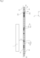
- the sensor arrangement according to the first embodiment serves to detect a distance D of a flat object 1 from a reference plane A0.
- the sensor arrangement according to Figure 1 comprises a carrier 10 and a coil element arrangement 12.
- the coil element arrangement 12 comprises a first coil element 14 for generating an excitation field, a second coil element 16 for detecting an alternating magnetic field generated by the first coil element 14 and dependent on the distance D, and a third coil element 20.1 for detecting the alternating magnetic field generated by a further coil element 18.
- the coil element arrangement 12 further comprises a fourth coil element 20.2 for detecting the alternating magnetic field generated by the further coil element 18 and independent of the distance D.
- the flat extended object 1 is, for example, a cuboid-shaped object and extends in an XY plane.
- the reference plane A0 extends parallel to the XY plane (cf. Figure 1 ).
- the carrier 10 comprises a circuit board with a first to third level A1 to A3 for carrying several excitation windings and sensing windings of the first to fourth coil elements 14, 16, 20.1, 20.2 and the further coil element 18. Furthermore, the carrier 10 comprises a fourth level A4 for carrying contact or connecting lines.
- the reference plane A0 corresponds to a plane (ie surface) of the carrier 10 facing the object 1.
- the first to fourth levels A1 to A4 of the sensor arrangement are Figure 1 shown.
- the first to fourth planes A1 to A4 each extend parallel to the reference plane A0.
- the reference plane A0 and the first to fourth planes A1 to A4 are arranged at a distance from one another in a direction Z perpendicular to the reference plane A0.
- the first to fourth planes A1 to A4 are arranged on a side of the reference plane A0 facing away from the object 1.
- the third coil element 20.1 comprises a first sensing winding 20.11 arranged in the first plane A1.
- the fourth coil element 20.2 comprises a second sensing winding 20.21 arranged in the third plane A3.
- the first sensing winding 20.11 and the second scanning winding 20.21 are arranged opposite each other (in the Z-direction) (cf. Figure 1 ).
- the further coil element 18 comprises an excitation winding (hereinafter "third excitation winding") 18.1 arranged in the second plane A2.
- the third excitation winding 18.1 is arranged between the first sensing winding 20.11 and the second sensing winding 20.21 (cf. Figure 1 ).
- the first scanning winding 20.11 and the second scanning winding 20.21 are of equal size, ie they have essentially the same extent in the XY plane.
- the first coil element 14 comprises a first excitation winding 14.1 arranged in the first plane A1 and a second excitation winding 14.2 arranged in the second plane A2.
- the first excitation winding 14.1 and the second excitation winding 14.2 are arranged opposite one another (in the Z direction) (cf. Figure 1 ).
- the second coil element 16 comprises a third scanning winding 16.1 arranged in the first plane A1 and a fourth scanning winding 16.2 arranged in the second plane A2.
- the third scanning winding 16.1 and the fourth scanning winding 16.2 are arranged opposite one another (in the Z direction) (cf. again Figure 1 ).
- the first and second excitation windings 14.1, 14.2 and the third and fourth scanning windings 16.1, 16.2 are each circular. Furthermore, in the plan views of Figure 2a to 2c shown that the third excitation winding 18.1 and the first and second sensing windings 20.11, 20.21 are each rectangular. The first and second excitation windings 14.1, 14.2 have the same direction of rotation, and the third and fourth sensing windings 16.1, 16.2 have the same direction of rotation.
- the first level A1 contains nodes P11, P12, P13 and lines 2.11, 2.12.
- the first excitation winding 14.1 is connected to the node P11 and the line 2.11.
- the line 2.12 is connected to the nodes P12, P13.
- the first level A1 contains nodes Q11, Q12.
- the third sensing winding 16.1 is connected to the nodes Q11, Q12.
- the first level A1 also contains nodes Q13, Q14.
- the first sensing winding 20.11 is connected to the nodes Q13, Q14.
- the second level A2 contains nodes P21, P22, P23, P24 and lines 2.21, 2.22.
- the second excitation winding 14.2 is connected to the node P21 and the line 2.21.
- the third excitation winding 18.1 is connected to the line 2.21 and the node P22.
- the line 2.22 is connected to the node P23.
- the second level A2 contains nodes Q21, Q22.
- the fourth sensing winding 16.2 is connected to the nodes Q21, Q22.
- the third level A3 contains nodes P31, P32 and a line 2.31.
- the line 2.31 is connected to the nodes P31, P32.
- the third level A3 contains nodes Q31, Q32, Q33 and lines 4.31, 4.32.
- the line 4.31 is connected to the nodes Q31, Q32.
- the line 4.32 is connected to the node Q33.
- the third level A3 also contains a node R31 and a line 6.31.
- the second sense winding 20.21 is connected to the node R31 and the line 6.31.
- the fourth level A4 contains nodes P41, P42 and a line 2.41.
- the line 2.41 is connected to the nodes P41, P42.
- the fourth level A4 contains nodes Q41, Q42, Q43, Q44, Q45 and lines 4.41, 4.42, 4.43.
- the line 4.41 is connected to the nodes Q41, Q42.
- the line 4.42 is connected to the node Q43.
- the line 4.43 is connected to the nodes Q44, Q45.
- the fourth level A4 also contains a node R41 and a line 6.41.
- the line 6.41 is connected to the node R41.
- the elements 16.1, 20.11; 16.2; 4.31, 4.32; 4.41, 4.42, 4.43 form a (second) line, ie through all elements 16.1, 20.11; 16.2; 4.31, 4.32; 4.41, 4.42, 4.43 the same (second) current flows.
- the elements 20.21, 6.31; 6.41 form a (third) line, ie the same (third) current flows through all elements 20.21, 6.31; 6.41.
- the second coil element 16 and the third coil element 20.1 are thus connected in series.
- the third coil element 20.1 is arranged in an X direction (ie longitudinal direction of the carrier 10) at such a distance from the object 1 that it is essentially not influenced by the alternating magnetic field generated by the first coil element 14.
- the same also applies to the fourth coil element 20.2.
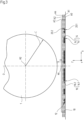
- the sensor arrangement according to the second embodiment serves to detect the distance D of the object 1, which is designed as a sphere, from the reference plane A0.
- the reference plane A0 extends parallel to the XY plane (cf. Figure 3 ).
- the sensor arrangement according to Figure 3 comprises the carrier 10 (ie circuit board) and the coil element arrangement 12.
- the coil element arrangement 12 comprises the first coil element 14 for generating the excitation field, the second coil element 16 for detecting the alternating magnetic field generated by the first coil element 14 and dependent on the distance D, and the third coil element 20.1 for detecting the alternating magnetic field generated by the first coil element 14.
- the coil element arrangement 12 also comprises the fourth coil element 20.2 for detecting the alternating magnetic field generated by the first coil element 14 and independent of the distance D.
- the reference plane A0 corresponds to a plane (i.e. surface) of the carrier 10 facing away from the object 1.
- the carrier 10 comprises the first and second planes A1, A2 for supporting several excitation windings and scanning windings of the first to fourth coil elements 14, 16, 20.1, 20.2.
- the third and fourth planes A3, A4 serve to support contact or connecting lines.
- the first to fourth planes A1 to A4 are arranged on a side of the reference plane A0 facing the object 1.
- the third coil element 20.1 comprises a first sensing winding 20.11 arranged in the first plane A1.
- the fourth coil element 20.2 comprises a second sensing winding 20.21 arranged in the second plane A2.
- the first sensing winding 20.11 and the second sensing winding 20.21 are arranged (in the Z direction) substantially opposite one another (cf. Figure 3 ).
- the first coil element 14 comprises a first excitation winding 14.1 arranged in the first plane A1 and a second excitation winding 14.2 arranged in the second plane A2.
- the first excitation winding 14.1 and the second excitation winding 14.2 are arranged opposite one another (in the Z direction) (cf. Figure 3 ).
- the second coil element 16 comprises a third scanning winding 16.1 arranged in the first plane A1 and a fourth scanning winding 16.2 arranged in the second plane A2.
- the third scanning winding 16.1 and the fourth scanning winding 16.2 are arranged opposite one another (in the Z direction) (cf. again Figure 3 ).
- the coil element arrangement 12 thus comprises an excitation winding 14.1 arranged in the first (common) plane A1 and two scanning windings 16.1, 20.11 or an excitation winding 14.2 arranged in the second (common) plane A2 and two scanning windings 16.2, 20.21.
- the first coil element 14 comprises the excitation winding 14.1 arranged in the first (common) plane A1
- the second and third coil elements 16, 20.1 comprise the two scanning windings 16.1, 20.11.
- This excitation winding 14.1 and these two scanning windings 16.1, 20.11 are arranged concentrically to one another (cf. Figure 4a ).
- the first coil element 14 comprises the excitation winding 14.2 arranged in the second (common) plane A2, and the second and fourth coil elements 16, 20.2 comprise the two scanning windings 16.2, 20.21.
- This excitation winding 14.2 and these two scanning windings 16.2, 20.21 are arranged concentrically to one another (cf. Figure 4b ).
- the first level A1 (cf. Figure 4a ) contains nodes P11', P12 ⁇ .
- the element 14.1 is connected to the nodes P11', P12 ⁇ .
- the first level A1 contains nodes Q11 ⁇ , Q12 ⁇ , Q13 ⁇ , Q14 ⁇ .
- the element 16.1 is connected to the nodes Q11', Q12'.
- the element 20.11 is connected to the nodes Q13', Q14'.
- the second level A2 (cf. Figure 4b ) contains nodes P21', P22', P23', P24' and a line 2.21'.
- the element 14.2 is connected to the nodes P21', P22'.
- the line 2.21' is connected to the nodes P23', P24'.
- the second level A2 contains nodes Q21', Q22', Q23', Q24' and a line 4.21'.
- the element 16.2 is connected to the nodes Q21', Q22'.
- the line 4.21' is connected to the nodes Q23', Q24'.
- the second level A2 contains also nodes R21', R22', R23'.
- the element 20.21 is connected to the nodes R21', R22', R23'.
- the third level A3 (cf. Figure 4c ) contains nodes P31', P32', P33', P34' and lines 2.31', 2.32'.
- Line 2.31' is connected to nodes P31', P32'.
- Line 2.32' is connected to nodes P33', P34'.
- the third level A3 contains nodes Q31', Q32', Q33', Q34' and lines 4.31', 4.32'.
- Line 4.31' is connected to nodes Q31', Q32'.
- Line 4.32' is connected to nodes Q33', Q34'.
- the third level A3 also contains nodes R31', R32', R33' and a line 6.31'.
- Line 6.31' is connected to nodes R31', R32', R33'.
- the fourth level A4 (cf. Figure 4d ) contains nodes P41', P42' and a line 2.41'.
- the line 2.41' is connected to the nodes P41', P42'.
- the fourth level A4 contains nodes Q41', Q42' and a line 4.41'.
- the line 4.41' is connected to the nodes Q41', Q42'.
- the elements ie excitation and scanning windings, are in turn connected to one another via the lines and nodes (as well as vias).
- the elements 14.1; 14.2, 2.21';2.31',2.32';2.41' form a (first) line.
- the elements 20.11, 16.1; 16.2, 4.21';4.31',4.32';4.41' form a (second) line.
- the elements 20.21; 6.31' form a (third) line.
- the first and second excitation windings 14.1, 14.2 have the same direction of rotation.
- the third and fourth scanning windings 16.1, 16.2 have the same direction of rotation.
- the first scanning winding 20.11 has a first (only) direction of rotation, ie all circular sections of the first scanning winding 20.11 have the same direction of rotation
- the second scanning winding 20.21 has a first and a second, different direction of rotation, ie the two circular sections of the second scanning winding 20.21 have a different direction of rotation.
- the first scanning winding 20.11 has three circular sections
- the second scanning winding 20.21 has only two circular sections.
- the object 1 is a sphere with a radius C.
- this radius C of the sphere is at least half as large and at most three times as large as a distance L1, L2 of the first or second scanning winding 20.11, 20.21 from a reference point O1, O2 lying on a reference axis O.
- the reference axis O runs perpendicular to the reference plane A0 through a center point M1 of the sensor arrangement and through a center point M2 of the sphere.
- the diameter of the sphere is at least half as large as the diameter of the first or second sensing winding 20.11, 20.21 and at most three times as large as the diameter of the first or second sensing winding 20.11, 20.21.
- the second embodiment achieves a distance measurement to a ball that is located in the middle of the sensor arrangement.
- Additional coils i.e. the first and second scanning windings 20.11 and 20.21, are arranged radially outside the respective excitation winding, i.e. the first and second excitation windings 14.1 and 14.2.
- the additional coil 20.21 is largely unaffected by the measuring object (i.e. ball). Since in the second embodiment all excitation and scanning windings are located next to each other in one area (in the XY plane), the structure (or the sensor arrangement according to Figure 3 ) is particularly compact. Thermal influences therefore have essentially the same effect on all excitation and scanning windings of the structure and can therefore be compensated for particularly easily.
- the first and second coil elements 14, 16 are inductively coupled depending on the relative position of the object 1 thereto or depending on the distance D. Furthermore, in the second exemplary embodiment, the first and third coil elements 14, 20.1 are inductively coupled depending on the relative position of the object 1 thereto or depending on the distance D, while the first and fourth coil elements 14, 20.2 are inductively coupled regardless of the relative position of the object 1 thereto or regardless of the distance D. Inductively coupled means that the excitation field generated by an excitation winding of the respective coil element generates eddy currents in the object 1, which act as a counterfield against the excitation field.
- a magnetic alternating field is generated due to the resulting alternating magnetic field, i.e. the detected excitation field influenced or uninfluenced by the opposing field, induces a voltage and generates a corresponding measuring signal, which is dependent or independent of the relative position to the object 1 (or the distance D).
- the first and second coil elements 14, 16 are inductively coupled depending on the distance D. Furthermore, in the first embodiment, the further and third coil elements 18, 20.1 and the further and fourth coil elements 18, 20.2 are each inductively coupled independently of the distance D.
- the excitation winding 14.2 and the sensing winding 16.2 can be omitted.
- the scanning winding 20.21 see the plane A2 in Figure 4b
- the scanning winding 20.11 see plane A1 in Figure 4a
- the scanning winding 20.21 is arranged together with the scanning winding 20.11 in the plane A1 instead of in the plane A2.
- the scanning winding 20.11 and the scanning winding 20.21 can have different radii (or different distances L1, L2).
- Figure 5 shows a cross-sectional view of an exemplary sensor module with the sensor arrangement according to Figure 3 .
- the sensor module has a further carrier 22 for carrying the sensor arrangement.
- the sensor arrangement is connected to the further carrier 22.
- an adhesive layer 24 is used, for example.
- the adhesive layer 24 is arranged between the further carrier 22 and the sensor arrangement (cf. Figure 5 ).
- the further carrier 22 is mounted on a support 23 which is Figure 5 not shown) facing away from the sensor arrangement and formed as a shielding layer.
- the further carrier 22 is a substrate made of ferrite material.
- Ferrite material has a high magnetic permeability and is electrically insulating, which prevents the generation of disturbing eddy currents in the further carrier 22.
- the sensor arrangement is shielded downwards (i.e. on a side facing away from the object 1) and only detects the distance to the object 1 that is approaching from above (i.e. on a side facing the object 1).
- the coil element arrangement 12 comprises a plurality of excitation windings 14.1, 14.2, 18.1 (optional) and sensing windings 16.1, 16.2, 20.11, 20.21 arranged in at least a first and second plane A1, A2.
- a node can be understood as a landing pad for a via or a through-plating.
- Vias or through-platings for the electrical contact between lines/windings on different levels are located at the location/position (XY position) of the nodes.
- nodes lying one above the other in the different levels in the Z direction are connected to one another via vias or through-platings.
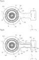
- Figure 6a shows a block diagram of an exemplary evaluation unit 100 with a unit 102 for performing an interpolation.
- Figure 6b shows a Block diagram of an exemplary evaluation unit 100 with a unit 102' for carrying out a division.
- the second coil element 16 and the third coil element 20.1 are designed to generate a first measurement signal 101-1 dependent on the distance D
- the fourth coil element 20.2 is designed to generate a second measurement signal 101-2 independent of the distance D.
- the evaluation unit 100 shown in Figure 6b is designed to determine the distance D depending on the first and second measurement signals 101-1, 101-2.
- the evaluation unit 100 generates an output signal 105 indicating the distance D.
- the evaluation unit 100 according to Figure 6a or 6b preferably comprises a unit 104 for linearization.
- the unit 102 is designed to generate an interpolated signal 103 depending on the first and second measurement signals 101-1, 101-2.
- the unit 104 applies a linearization to the interpolated signal 103 so that the output signal 105 is obtained.
- the unit 102 is a component (e.g. inductive ASIC) that is used in known incremental position measuring devices.
- the unit 102 is designed to receive two incremental signals (e.g. sine-cosine pair) that are phase-shifted by 90° at the input of the unit 102 and to output a position at the output of the unit 102.
- the functionality of the unit 102 ie interpolation is known.
- the interpolated signal 103 corresponds to the position output at the output of the unit 102.
- the unit 102 (here the aforementioned component) receives the first measurement signal 101-1 (e.g. a signal that is essentially linear over the distance) and the second measurement signal 101-2 (e.g. a signal that is essentially constant over the distance) instead of phase-shifted incremental signals (e.g. a sine-cosine pair), there is no linear relationship between the position and an interpolation value (phase signal value) after the interpolation.
- the unit 104 can make a correction of the interpolated signal 103 to obtain a linear relationship between the position and the interpolation value.
- the position ie the distance D
- the unit 102' is designed to generate a standardized signal 103 as a function of the first and second measurement signals 101-1, 101-2.
- the unit 104 applies a linearization to the standardized signal 103 so that the output signal 105 is obtained.
- the evaluation unit 100 is designed to calculate the first and second measurement signals 101-1, 101-2 by forming the arctangent (e.g. by the unit 102 in Figure 6a ) or a division (e.g. by the unit 102' in Figure 6b ) to obtain the distance D.
- the third and fourth coil elements 20.1, 20.2 can each also be referred to as pickup coils.
- the third coil element 20.1 which is coupled to the excitation field, can cause a signal change or offset reduction.
- the fourth coil element 20.2 (“Pickup coil 2") can generate the reference signal, which can be used to standardize the offset-corrected signal.
- the standardization can compensate for the influence of temperature on the excitation current (temperature compensation).
- the pickup coil 1 and pickup coil 2 can essentially collect the excitation field twice (whereby the standardization can eliminate effects that affect the offset-corrected signal and the reference signal equally and lead to corresponding signal changes, for example by forming the arctangent, and essentially cancel each other out).
- the pickup coil 2 should not be influenced by object 1.
- a change in temperature can typically change the resistance of the cables, among other things, and in this case
- the frequency of the excitation current is also important. If the excitation current changes, this has an influence on the strength of the excitation field and thus also on the induced voltage in the receiving coils (scanning turns) and thus on the measured position (ie distance D) of the object 1.
- the invention makes it possible to reduce this influence. To this end, use is made in particular of the aforementioned standardization of the excitation current.
- temperature compensation can be realized without the use of additional temperature sensors.
- the sensor arrangement according to the invention can be used in a laser tracker based on distance measurement for determining three-dimensional coordinates in space.
Landscapes
- Physics & Mathematics (AREA)
- Engineering & Computer Science (AREA)
- Remote Sensing (AREA)
- Life Sciences & Earth Sciences (AREA)
- Electromagnetism (AREA)
- Environmental & Geological Engineering (AREA)
- Geology (AREA)
- General Life Sciences & Earth Sciences (AREA)
- General Physics & Mathematics (AREA)
- Geophysics (AREA)
- Measurement Of Length, Angles, Or The Like Using Electric Or Magnetic Means (AREA)
- Transmission And Conversion Of Sensor Element Output (AREA)
Claims (15)
- Ensemble de capteurs destiné à détecter des champs magnétiques alternatifs qui, d'une part, dépendent d'une distance (D) d'un objet (1) à un plan de référence (A0) ou qui, d'autre part, sont indépendants de la distance (D), ledit ensemble de capteurs comprenantun support (10), etun ensemble d'éléments de bobine (12) comportant au moins un premier élément de bobine (14) destiné à générer un champ d'excitation, un deuxième élément de bobine (16) destiné à détecter un champ magnétique alternatif généré par le premier élément de bobine (14) et dépendant de la distance (D), et un troisième élément de bobine (20.1) destiné à détecter le champ magnétique alternatif généré par le premier élément de bobine (14),caractérisé en ce quel'ensemble d'éléments de bobine (12) comprend un quatrième élément de bobine (20.2) destiné à détecter le champ magnétique alternatif généré par le premier élément de bobine (14) et indépendant de la distance (D),le deuxième élément de bobine (16) et le troisième élément de bobine (20.1) sont montés en série,le deuxième élément de bobine (16) et le troisième élément de bobine (20.1) sont conçus pour générer un premier signal de mesure (101-1) qui dépend de la distance (D), etle quatrième élément de bobine (20.2) est conçu pour générer un deuxième signal de mesure (101-2) indépendant de la distance (D).
- Ensemble de capteurs selon la revendication 1, l'ensemble de capteurs comprenant une unité d'évaluation (100), l'unité d'évaluation (100) étant conçu pour déterminer la distance (D) en fonction des premier et deuxième signaux de mesure (101-1, 101-2).
- Ensemble de capteurs selon la revendication 2, l'unité d'évaluation (100) étant conçue pour combiner les premier et deuxième signaux de mesure (101-1, 101-2) par formation de l'arc tangente ou par division afin d'obtenir la distance (D).
- Ensemble de capteurs selon l'une des revendications précédentes, l'ensemble d'éléments de bobine (12) comprenant une pluralité d'enroulements d'excitation (14.1, 14.2) et d'enroulements de balayage (16.1, 16.2, 20.11, 20.21) disposés dans au moins un premier et un deuxième plan (A1, A2), le premier plan (A1) et le deuxième plan (A2) s'étendant chacun parallèlement au plan de référence (A0), le premier et le deuxième plan (A1, A2) étant disposés à distance l'un de l'autre dans une direction (Z) perpendiculaire au plan de référence (A0).
- Ensemble de capteurs selon la revendication 4, le troisième élément de bobine (20.1) comprenant un premier enroulement de balayage (20.11) disposé dans le premier plan (A1), le quatrième élément de bobine (20.2) comprenant un deuxième enroulement de balayage (20.21) disposé dans le deuxième ou un troisième plan (A2, A3), le troisième plan (A3) s'étendant parallèlement au plan de référence (A0), le deuxième et le troisième plan (A2, A3) étant disposés à distance l'un de l'autre dans la direction (Z) perpendiculaire au plan de référence (A0), le premier enroulement de balayage (20.11) et le deuxième enroulement de balayage (20.21) étant disposés l'un en face de l'autre.
- Ensemble de capteurs selon l'une des revendications précédentes, l'ensemble d'éléments de bobine (12) comprenant un enroulement d'excitation (14.1, 14.2) disposé dans un plan commun (A1, A2) et deux enroulements de balayage (16.1, 20.11 ; 16.2, 20.21), le plan commun (A1, A2) s'étendant parallèlement au plan de référence (A0), le premier élément de bobine (14) comprenant l'enroulement d'excitation (14.1, 14.2) disposé dans le plan commun (A1, A2) et les deuxième et troisième éléments de bobine (16, 20.1) ou les deuxième et quatrième éléments de bobine (16, 20.2) comprenant les deux enroulements de balayage (16.1, 20.11 ; 16.2, 20.21), cet enroulement d'excitation (14.1, 14.2) et ces deux enroulements de balayage (16.1, 20.11 ; 16.2, 20.21) étant disposés concentriquement l'un à l'autre.
- Ensemble de capteurs selon la revendication 6, l'un de ces deux enroulements de balayage (16.1, 20.11 ; 16.2, 20.21) étant disposé à l'intérieur de cet enroulement d'excitation (14.1, 14.2) et l'autre de ces deux enroulements de balayage (16.1, 20.11 ; 16.2, 20.21) étant disposé à l'extérieur de cet enroulement d'excitation (14.1, 14.2).
- Ensemble de capteurs selon l'une des revendications précédentes, le troisième élément de bobine (20.1) étant conçu pour générer un troisième signal de mesure, le troisième élément de bobine (20.1) et le quatrième élément de bobine (20.2) étant conçus de telle sorte qu'une première intensité de signal d'un signal de mesure du quatrième élément de bobine (20.2) soit inférieure ou égale à une deuxième intensité de signal du troisième signal de mesure, de préférence la première intensité du signal étant inférieure à 25 % ou inférieure à 10 % de la deuxième intensité du signal.
- Ensemble de capteurs selon l'une des revendications précédentes, l'objet (1) étant une sphère, un rayon (C) de la sphère étant égal à au moins la moitié et au plus au triple d'une distance (L1, L2) d'un enroulement de balayage (20.11, 20.21) du troisième ou du quatrième élément de bobine (20.1, 20.2) à un point de référence (O1, O2) situé sur un axe de référence (O), l'axe de référence (O) s'étendant perpendiculairement au plan de référence (A0) passant par un point central (M1) de l'ensemble de capteurs et passant par un point central (M2) de la sphère.
- Ensemble de capteurs selon l'une des revendications précédentes, le support (10) étant une carte de circuit imprimé comportant au moins deux plans (A1, A2) destinés à supporter une pluralité d'enroulements d'excitation et d'enroulements de balayage des premier à quatrième éléments de bobine (14, 16, 20.1, 20.2).
- Module de capteur comprenant un ensemble de capteurs selon l'une des revendications précédentes, le module de capteurs comportant un autre support (22) destiné à porter l'ensemble de capteurs, l'ensemble de capteurs étant relié à l'autre support (22), l'autre support (22) étant disposé sur un côté de l'ensemble de capteurs qui est opposé à l'objet (1) et étant conçu comme une couche de protection.
- Ensemble de capteurs destiné à détecter des champs magnétiques alternatifs qui, d'une part, dépendent d'une distance (D) d'un objet (1) à un plan de référence (A0) ou qui, d'autre part, sont indépendants de la distance (D), ledit ensemble de capteurs comprenantun support (10), etun ensemble d'éléments de bobine (12) comportant au moins un premier élément de bobine (14) destiné à générer un champ d'excitation, un deuxième élément de bobine (16) destiné à détecter un champ magnétique alternatif généré par le premier élément de bobine (14) et dépendant de la distance (D) et un troisième élément de bobine (20.1) destiné à détecter le champ magnétique alternatif généré par un autre élément de bobine (18), caractérisé en ce quel'ensemble d'éléments de bobine (12) comprend un quatrième élément de bobine (20.2) destiné à détecter le champ magnétique alternatif généré par l'autre élément de bobine (18) et indépendant de la distance (D),le deuxième élément de bobine (16) et le troisième élément de bobine (20.1) sont montés en série,le deuxième élément de bobine (16) et le troisième élément de bobine (20.1) sont conçus pour générer un premier signal de mesure (101-1) qui dépend de la distance (D), etle quatrième élément de bobine (20.2) est conçu pour générer un deuxième signal de mesure (101-2) indépendant de la distance (D).
- Ensemble de capteurs selon la revendication 12, l'autre élément de bobine (18) comprenant un enroulement d'excitation (18.1) disposé dans le deuxième niveau (A2), cet enroulement d'excitation (18.1) étant disposé entre le premier enroulement de balayage (20.11) et le deuxième enroulement de balayage (20.21).
- Ensemble de capteurs selon la revendication 13, le premier enroulement de balayage (20.11) et le deuxième enroulement de balayage (20.21) étant de même dimension.
- Utilisation d'un ensemble de capteurs selon la revendication 1 ou 12 pour détecter la distance (D) de l'objet (1) au plan de référence (A0).
Priority Applications (2)
| Application Number | Priority Date | Filing Date | Title |
|---|---|---|---|
| EP21171125.4A EP4083663B1 (fr) | 2021-04-29 | 2021-04-29 | Capteur pour détecter une distance entre un objet et un plan de référence |
| DE102022201936.9A DE102022201936A1 (de) | 2021-04-29 | 2022-02-24 | Sensoranordnung zum Erfassen eines Abstands eines Objekts von einer Referenzebene |
Applications Claiming Priority (1)
| Application Number | Priority Date | Filing Date | Title |
|---|---|---|---|
| EP21171125.4A EP4083663B1 (fr) | 2021-04-29 | 2021-04-29 | Capteur pour détecter une distance entre un objet et un plan de référence |
Publications (2)
| Publication Number | Publication Date |
|---|---|
| EP4083663A1 EP4083663A1 (fr) | 2022-11-02 |
| EP4083663B1 true EP4083663B1 (fr) | 2024-06-05 |
Family
ID=75746208
Family Applications (1)
| Application Number | Title | Priority Date | Filing Date |
|---|---|---|---|
| EP21171125.4A Active EP4083663B1 (fr) | 2021-04-29 | 2021-04-29 | Capteur pour détecter une distance entre un objet et un plan de référence |
Country Status (2)
| Country | Link |
|---|---|
| EP (1) | EP4083663B1 (fr) |
| DE (1) | DE102022201936A1 (fr) |
Family Cites Families (6)
| Publication number | Priority date | Publication date | Assignee | Title |
|---|---|---|---|---|
| DE3476035D1 (en) * | 1983-07-05 | 1989-02-16 | Elektroniktechnologie Get | Inductive sensor device and measuring device for using the same |
| DE10362165A1 (de) * | 2003-04-23 | 2006-12-28 | Werner Turck Gmbh & Co. Kg | Induktiver Näherungsschalter |
| DE10350733B4 (de) | 2003-10-20 | 2006-04-27 | Werner Turck Gmbh & Co. Kg | Induktiver Näherungsschalter mit Differenzspulenanordnung |
| US20150002157A1 (en) * | 2012-01-27 | 2015-01-01 | Texas A&M University System | Transient electromagnetic geophysics system with cooperative source(s) |
| DE102013222936A1 (de) | 2012-11-09 | 2014-05-15 | Elmos Semiconductor Ag | Spule für einen induktiven Sensor und Schaltung zu dessen Ansteuerung |
| DE102013226203A1 (de) | 2013-12-17 | 2015-06-18 | Robert Bosch Gmbh | Offsetkompensierte Positionsmessvorrichtung |
-
2021
- 2021-04-29 EP EP21171125.4A patent/EP4083663B1/fr active Active
-
2022
- 2022-02-24 DE DE102022201936.9A patent/DE102022201936A1/de active Pending
Also Published As
| Publication number | Publication date |
|---|---|
| EP4083663A1 (fr) | 2022-11-02 |
| DE102022201936A1 (de) | 2022-11-03 |
Similar Documents
| Publication | Publication Date | Title |
|---|---|---|
| EP1110094B1 (fr) | Dispositif et procede de formation d'au mois un gradient de champ magnetique au travers d'un conducteur rectiligne | |
| DE69717188T2 (de) | Mit Magnetfeldveränderungen arbeitender Bewegungs- und Positionsdetektor | |
| DE102004047189A1 (de) | Sensor zur Ortung metallischer Objekte sowie Verfahren zur Auswertung von Messsignalen eines solchen Sensors | |
| EP1295089A1 (fr) | Dispositif pour mesurer le deplacement sans contact, notamment pour saisir la position et le mouvement | |
| DE102006034579A1 (de) | Stromerfassungsvorrichtung und Verfahren zur Stromerfassung | |
| DE112021005057T5 (de) | Hochauflösender induktiver winkelsensor und zugehöriges verfahren zur verwendung | |
| EP1797464B1 (fr) | Détecteur pour la localisation d'objets métalliques | |
| DE102018111011A1 (de) | Magnetfeldsensorvorrichtung | |
| EP4306911A1 (fr) | Capteur inductif pour détecter une position | |
| DE102021110370A1 (de) | Stromsensor | |
| EP1219933B1 (fr) | Sonde à courant de Foucault différentielle | |
| DE102013226203A1 (de) | Offsetkompensierte Positionsmessvorrichtung | |
| WO2017198468A1 (fr) | Capteur de déplacement linéaire autorisant le basculement | |
| WO2007051801A1 (fr) | Agencement de mesure d'un champ magnetique | |
| DE2701857C2 (fr) | ||
| DE19512374A1 (de) | Resistiver Neigungssensor | |
| DE102011085876A1 (de) | Objektfinder | |
| DE102017215722B4 (de) | Einrichtung zur Messung von Kommutierungsströmen schnell schaltender Halbleiterbauelemente | |
| DE102022201936A1 (de) | Sensoranordnung zum Erfassen eines Abstands eines Objekts von einer Referenzebene | |
| DE102019210301A1 (de) | Sensoranordnung zum Erfassen einer Auslenkung einer Drahtelektrode | |
| DE102022114508A1 (de) | Induktiver Linearwegsensor sowie Fahrzeug mit einem induktiven Linearwegsensor | |
| EP0875734A1 (fr) | Capteur de position inductif | |
| DE4406417A1 (de) | Einrichtung zum Messen eines Weges oder eines Winkels | |
| DE4414070A1 (de) | Kapazitiver Drehmomentsensor | |
| DE4443464C2 (de) | Spulenanordnung |
Legal Events
| Date | Code | Title | Description |
|---|---|---|---|
| PUAI | Public reference made under article 153(3) epc to a published international application that has entered the european phase |
Free format text: ORIGINAL CODE: 0009012 |
|
| STAA | Information on the status of an ep patent application or granted ep patent |
Free format text: STATUS: THE APPLICATION HAS BEEN PUBLISHED |
|
| AK | Designated contracting states |
Kind code of ref document: A1 Designated state(s): AL AT BE BG CH CY CZ DE DK EE ES FI FR GB GR HR HU IE IS IT LI LT LU LV MC MK MT NL NO PL PT RO RS SE SI SK SM TR |
|
| STAA | Information on the status of an ep patent application or granted ep patent |
Free format text: STATUS: REQUEST FOR EXAMINATION WAS MADE |
|
| 17P | Request for examination filed |
Effective date: 20230502 |
|
| RBV | Designated contracting states (corrected) |
Designated state(s): AL AT BE BG CH CY CZ DE DK EE ES FI FR GB GR HR HU IE IS IT LI LT LU LV MC MK MT NL NO PL PT RO RS SE SI SK SM TR |
|
| GRAP | Despatch of communication of intention to grant a patent |
Free format text: ORIGINAL CODE: EPIDOSNIGR1 |
|
| STAA | Information on the status of an ep patent application or granted ep patent |
Free format text: STATUS: GRANT OF PATENT IS INTENDED |
|
| INTG | Intention to grant announced |
Effective date: 20240102 |
|
| GRAS | Grant fee paid |
Free format text: ORIGINAL CODE: EPIDOSNIGR3 |
|
| GRAA | (expected) grant |
Free format text: ORIGINAL CODE: 0009210 |
|
| STAA | Information on the status of an ep patent application or granted ep patent |
Free format text: STATUS: THE PATENT HAS BEEN GRANTED |
|
| AK | Designated contracting states |
Kind code of ref document: B1 Designated state(s): AL AT BE BG CH CY CZ DE DK EE ES FI FR GB GR HR HU IE IS IT LI LT LU LV MC MK MT NL NO PL PT RO RS SE SI SK SM TR |
|
| REG | Reference to a national code |
Ref country code: CH Ref legal event code: EP |
|
| REG | Reference to a national code |
Ref country code: DE Ref legal event code: R096 Ref document number: 502021003905 Country of ref document: DE |
|
| REG | Reference to a national code |
Ref country code: IE Ref legal event code: FG4D Free format text: LANGUAGE OF EP DOCUMENT: GERMAN |
|
| REG | Reference to a national code |
Ref country code: LT Ref legal event code: MG9D |
|
| PG25 | Lapsed in a contracting state [announced via postgrant information from national office to epo] |
Ref country code: BG Free format text: LAPSE BECAUSE OF FAILURE TO SUBMIT A TRANSLATION OF THE DESCRIPTION OR TO PAY THE FEE WITHIN THE PRESCRIBED TIME-LIMIT Effective date: 20240605 |
|
| REG | Reference to a national code |
Ref country code: NL Ref legal event code: MP Effective date: 20240605 |
|
| PG25 | Lapsed in a contracting state [announced via postgrant information from national office to epo] |
Ref country code: FI Free format text: LAPSE BECAUSE OF FAILURE TO SUBMIT A TRANSLATION OF THE DESCRIPTION OR TO PAY THE FEE WITHIN THE PRESCRIBED TIME-LIMIT Effective date: 20240605 Ref country code: HR Free format text: LAPSE BECAUSE OF FAILURE TO SUBMIT A TRANSLATION OF THE DESCRIPTION OR TO PAY THE FEE WITHIN THE PRESCRIBED TIME-LIMIT Effective date: 20240605 |
|
| PG25 | Lapsed in a contracting state [announced via postgrant information from national office to epo] |
Ref country code: GR Free format text: LAPSE BECAUSE OF FAILURE TO SUBMIT A TRANSLATION OF THE DESCRIPTION OR TO PAY THE FEE WITHIN THE PRESCRIBED TIME-LIMIT Effective date: 20240906 |
|
| PG25 | Lapsed in a contracting state [announced via postgrant information from national office to epo] |
Ref country code: ES Free format text: LAPSE BECAUSE OF FAILURE TO SUBMIT A TRANSLATION OF THE DESCRIPTION OR TO PAY THE FEE WITHIN THE PRESCRIBED TIME-LIMIT Effective date: 20240605 |
|
| PG25 | Lapsed in a contracting state [announced via postgrant information from national office to epo] |
Ref country code: LV Free format text: LAPSE BECAUSE OF FAILURE TO SUBMIT A TRANSLATION OF THE DESCRIPTION OR TO PAY THE FEE WITHIN THE PRESCRIBED TIME-LIMIT Effective date: 20240605 |
|
| PG25 | Lapsed in a contracting state [announced via postgrant information from national office to epo] |
Ref country code: NO Free format text: LAPSE BECAUSE OF FAILURE TO SUBMIT A TRANSLATION OF THE DESCRIPTION OR TO PAY THE FEE WITHIN THE PRESCRIBED TIME-LIMIT Effective date: 20240905 Ref country code: LV Free format text: LAPSE BECAUSE OF FAILURE TO SUBMIT A TRANSLATION OF THE DESCRIPTION OR TO PAY THE FEE WITHIN THE PRESCRIBED TIME-LIMIT Effective date: 20240605 Ref country code: HR Free format text: LAPSE BECAUSE OF FAILURE TO SUBMIT A TRANSLATION OF THE DESCRIPTION OR TO PAY THE FEE WITHIN THE PRESCRIBED TIME-LIMIT Effective date: 20240605 Ref country code: GR Free format text: LAPSE BECAUSE OF FAILURE TO SUBMIT A TRANSLATION OF THE DESCRIPTION OR TO PAY THE FEE WITHIN THE PRESCRIBED TIME-LIMIT Effective date: 20240906 Ref country code: FI Free format text: LAPSE BECAUSE OF FAILURE TO SUBMIT A TRANSLATION OF THE DESCRIPTION OR TO PAY THE FEE WITHIN THE PRESCRIBED TIME-LIMIT Effective date: 20240605 Ref country code: ES Free format text: LAPSE BECAUSE OF FAILURE TO SUBMIT A TRANSLATION OF THE DESCRIPTION OR TO PAY THE FEE WITHIN THE PRESCRIBED TIME-LIMIT Effective date: 20240605 Ref country code: BG Free format text: LAPSE BECAUSE OF FAILURE TO SUBMIT A TRANSLATION OF THE DESCRIPTION OR TO PAY THE FEE WITHIN THE PRESCRIBED TIME-LIMIT Effective date: 20240605 Ref country code: RS Free format text: LAPSE BECAUSE OF FAILURE TO SUBMIT A TRANSLATION OF THE DESCRIPTION OR TO PAY THE FEE WITHIN THE PRESCRIBED TIME-LIMIT Effective date: 20240905 |
|
| PG25 | Lapsed in a contracting state [announced via postgrant information from national office to epo] |
Ref country code: NL Free format text: LAPSE BECAUSE OF FAILURE TO SUBMIT A TRANSLATION OF THE DESCRIPTION OR TO PAY THE FEE WITHIN THE PRESCRIBED TIME-LIMIT Effective date: 20240605 |
|
| PG25 | Lapsed in a contracting state [announced via postgrant information from national office to epo] |
Ref country code: NL Free format text: LAPSE BECAUSE OF FAILURE TO SUBMIT A TRANSLATION OF THE DESCRIPTION OR TO PAY THE FEE WITHIN THE PRESCRIBED TIME-LIMIT Effective date: 20240605 |
|
| PG25 | Lapsed in a contracting state [announced via postgrant information from national office to epo] |
Ref country code: PT Free format text: LAPSE BECAUSE OF FAILURE TO SUBMIT A TRANSLATION OF THE DESCRIPTION OR TO PAY THE FEE WITHIN THE PRESCRIBED TIME-LIMIT Effective date: 20241007 |
|
| PG25 | Lapsed in a contracting state [announced via postgrant information from national office to epo] |
Ref country code: PT Free format text: LAPSE BECAUSE OF FAILURE TO SUBMIT A TRANSLATION OF THE DESCRIPTION OR TO PAY THE FEE WITHIN THE PRESCRIBED TIME-LIMIT Effective date: 20241007 |
|
| PG25 | Lapsed in a contracting state [announced via postgrant information from national office to epo] |
Ref country code: PL Free format text: LAPSE BECAUSE OF FAILURE TO SUBMIT A TRANSLATION OF THE DESCRIPTION OR TO PAY THE FEE WITHIN THE PRESCRIBED TIME-LIMIT Effective date: 20240605 |
|
| PG25 | Lapsed in a contracting state [announced via postgrant information from national office to epo] |
Ref country code: EE Free format text: LAPSE BECAUSE OF FAILURE TO SUBMIT A TRANSLATION OF THE DESCRIPTION OR TO PAY THE FEE WITHIN THE PRESCRIBED TIME-LIMIT Effective date: 20240605 |
|
| PG25 | Lapsed in a contracting state [announced via postgrant information from national office to epo] |
Ref country code: IS Free format text: LAPSE BECAUSE OF FAILURE TO SUBMIT A TRANSLATION OF THE DESCRIPTION OR TO PAY THE FEE WITHIN THE PRESCRIBED TIME-LIMIT Effective date: 20241005 |
|
| PG25 | Lapsed in a contracting state [announced via postgrant information from national office to epo] |
Ref country code: CZ Free format text: LAPSE BECAUSE OF FAILURE TO SUBMIT A TRANSLATION OF THE DESCRIPTION OR TO PAY THE FEE WITHIN THE PRESCRIBED TIME-LIMIT Effective date: 20240605 |
|
| PG25 | Lapsed in a contracting state [announced via postgrant information from national office to epo] |
Ref country code: RO Free format text: LAPSE BECAUSE OF FAILURE TO SUBMIT A TRANSLATION OF THE DESCRIPTION OR TO PAY THE FEE WITHIN THE PRESCRIBED TIME-LIMIT Effective date: 20240605 Ref country code: SK Free format text: LAPSE BECAUSE OF FAILURE TO SUBMIT A TRANSLATION OF THE DESCRIPTION OR TO PAY THE FEE WITHIN THE PRESCRIBED TIME-LIMIT Effective date: 20240605 |
|
| PG25 | Lapsed in a contracting state [announced via postgrant information from national office to epo] |
Ref country code: SM Free format text: LAPSE BECAUSE OF FAILURE TO SUBMIT A TRANSLATION OF THE DESCRIPTION OR TO PAY THE FEE WITHIN THE PRESCRIBED TIME-LIMIT Effective date: 20240605 |
|
| PG25 | Lapsed in a contracting state [announced via postgrant information from national office to epo] |
Ref country code: SM Free format text: LAPSE BECAUSE OF FAILURE TO SUBMIT A TRANSLATION OF THE DESCRIPTION OR TO PAY THE FEE WITHIN THE PRESCRIBED TIME-LIMIT Effective date: 20240605 Ref country code: SK Free format text: LAPSE BECAUSE OF FAILURE TO SUBMIT A TRANSLATION OF THE DESCRIPTION OR TO PAY THE FEE WITHIN THE PRESCRIBED TIME-LIMIT Effective date: 20240605 Ref country code: RO Free format text: LAPSE BECAUSE OF FAILURE TO SUBMIT A TRANSLATION OF THE DESCRIPTION OR TO PAY THE FEE WITHIN THE PRESCRIBED TIME-LIMIT Effective date: 20240605 Ref country code: PL Free format text: LAPSE BECAUSE OF FAILURE TO SUBMIT A TRANSLATION OF THE DESCRIPTION OR TO PAY THE FEE WITHIN THE PRESCRIBED TIME-LIMIT Effective date: 20240605 Ref country code: IS Free format text: LAPSE BECAUSE OF FAILURE TO SUBMIT A TRANSLATION OF THE DESCRIPTION OR TO PAY THE FEE WITHIN THE PRESCRIBED TIME-LIMIT Effective date: 20241005 Ref country code: EE Free format text: LAPSE BECAUSE OF FAILURE TO SUBMIT A TRANSLATION OF THE DESCRIPTION OR TO PAY THE FEE WITHIN THE PRESCRIBED TIME-LIMIT Effective date: 20240605 Ref country code: CZ Free format text: LAPSE BECAUSE OF FAILURE TO SUBMIT A TRANSLATION OF THE DESCRIPTION OR TO PAY THE FEE WITHIN THE PRESCRIBED TIME-LIMIT Effective date: 20240605 |
|
| PG25 | Lapsed in a contracting state [announced via postgrant information from national office to epo] |
Ref country code: IT Free format text: LAPSE BECAUSE OF FAILURE TO SUBMIT A TRANSLATION OF THE DESCRIPTION OR TO PAY THE FEE WITHIN THE PRESCRIBED TIME-LIMIT Effective date: 20240605 |
|
| REG | Reference to a national code |
Ref country code: DE Ref legal event code: R097 Ref document number: 502021003905 Country of ref document: DE |
|
| PLBE | No opposition filed within time limit |
Free format text: ORIGINAL CODE: 0009261 |
|
| STAA | Information on the status of an ep patent application or granted ep patent |
Free format text: STATUS: NO OPPOSITION FILED WITHIN TIME LIMIT |
|
| PG25 | Lapsed in a contracting state [announced via postgrant information from national office to epo] |
Ref country code: DK Free format text: LAPSE BECAUSE OF FAILURE TO SUBMIT A TRANSLATION OF THE DESCRIPTION OR TO PAY THE FEE WITHIN THE PRESCRIBED TIME-LIMIT Effective date: 20240605 |
|
| 26N | No opposition filed |
Effective date: 20250306 |
|
| PGFP | Annual fee paid to national office [announced via postgrant information from national office to epo] |
Ref country code: DE Payment date: 20250422 Year of fee payment: 5 |
|
| PGFP | Annual fee paid to national office [announced via postgrant information from national office to epo] |
Ref country code: CH Payment date: 20250501 Year of fee payment: 5 |
|
| PGFP | Annual fee paid to national office [announced via postgrant information from national office to epo] |
Ref country code: AT Payment date: 20250721 Year of fee payment: 5 |
|
| PG25 | Lapsed in a contracting state [announced via postgrant information from national office to epo] |
Ref country code: SE Free format text: LAPSE BECAUSE OF FAILURE TO SUBMIT A TRANSLATION OF THE DESCRIPTION OR TO PAY THE FEE WITHIN THE PRESCRIBED TIME-LIMIT Effective date: 20240605 |
|
| PG25 | Lapsed in a contracting state [announced via postgrant information from national office to epo] |
Ref country code: LU Free format text: LAPSE BECAUSE OF NON-PAYMENT OF DUE FEES Effective date: 20250429 |
|
| PG25 | Lapsed in a contracting state [announced via postgrant information from national office to epo] |
Ref country code: MC Free format text: LAPSE BECAUSE OF FAILURE TO SUBMIT A TRANSLATION OF THE DESCRIPTION OR TO PAY THE FEE WITHIN THE PRESCRIBED TIME-LIMIT Effective date: 20240605 |
|
| GBPC | Gb: european patent ceased through non-payment of renewal fee |
Effective date: 20250429 |
|
| REG | Reference to a national code |
Ref country code: BE Ref legal event code: MM Effective date: 20250430 |
|
| REG | Reference to a national code |
Ref country code: CH Ref legal event code: R17 Free format text: ST27 STATUS EVENT CODE: U-0-0-R10-R17 (AS PROVIDED BY THE NATIONAL OFFICE) Effective date: 20260108 |
|
| PG25 | Lapsed in a contracting state [announced via postgrant information from national office to epo] |
Ref country code: GB Free format text: LAPSE BECAUSE OF NON-PAYMENT OF DUE FEES Effective date: 20250429 |
|
| PG25 | Lapsed in a contracting state [announced via postgrant information from national office to epo] |
Ref country code: FR Free format text: LAPSE BECAUSE OF NON-PAYMENT OF DUE FEES Effective date: 20250430 |
|
| PG25 | Lapsed in a contracting state [announced via postgrant information from national office to epo] |
Ref country code: BE Free format text: LAPSE BECAUSE OF NON-PAYMENT OF DUE FEES Effective date: 20250430 |
|
| PG25 | Lapsed in a contracting state [announced via postgrant information from national office to epo] |
Ref country code: IE Free format text: LAPSE BECAUSE OF NON-PAYMENT OF DUE FEES Effective date: 20250429 |
|
| REG | Reference to a national code |
Ref country code: CH Ref legal event code: U11 Free format text: ST27 STATUS EVENT CODE: U-0-0-U10-U11 (AS PROVIDED BY THE NATIONAL OFFICE) Effective date: 20260501 |