EP4083989B1 - Dispositif d'affichage, puce d'attaque et dispositif électronique - Google Patents
Dispositif d'affichage, puce d'attaque et dispositif électronique Download PDFInfo
- Publication number
- EP4083989B1 EP4083989B1 EP21874316.9A EP21874316A EP4083989B1 EP 4083989 B1 EP4083989 B1 EP 4083989B1 EP 21874316 A EP21874316 A EP 21874316A EP 4083989 B1 EP4083989 B1 EP 4083989B1
- Authority
- EP
- European Patent Office
- Prior art keywords
- signal line
- signal
- electrically connected
- shift
- detection
- Prior art date
- Legal status (The legal status is an assumption and is not a legal conclusion. Google has not performed a legal analysis and makes no representation as to the accuracy of the status listed.)
- Active
Links
Images







Classifications
-
- G—PHYSICS
- G09—EDUCATION; CRYPTOGRAPHY; DISPLAY; ADVERTISING; SEALS
- G09G—ARRANGEMENTS OR CIRCUITS FOR CONTROL OF INDICATING DEVICES USING STATIC MEANS TO PRESENT VARIABLE INFORMATION
- G09G3/00—Control arrangements or circuits, of interest only in connection with visual indicators other than cathode-ray tubes
- G09G3/20—Control arrangements or circuits, of interest only in connection with visual indicators other than cathode-ray tubes for presentation of an assembly of a number of characters, e.g. a page, by composing the assembly by combination of individual elements arranged in a matrix no fixed position being assigned to or needed to be assigned to the individual characters or partial characters
- G09G3/22—Control arrangements or circuits, of interest only in connection with visual indicators other than cathode-ray tubes for presentation of an assembly of a number of characters, e.g. a page, by composing the assembly by combination of individual elements arranged in a matrix no fixed position being assigned to or needed to be assigned to the individual characters or partial characters using controlled light sources
- G09G3/30—Control arrangements or circuits, of interest only in connection with visual indicators other than cathode-ray tubes for presentation of an assembly of a number of characters, e.g. a page, by composing the assembly by combination of individual elements arranged in a matrix no fixed position being assigned to or needed to be assigned to the individual characters or partial characters using controlled light sources using electroluminescent panels
- G09G3/32—Control arrangements or circuits, of interest only in connection with visual indicators other than cathode-ray tubes for presentation of an assembly of a number of characters, e.g. a page, by composing the assembly by combination of individual elements arranged in a matrix no fixed position being assigned to or needed to be assigned to the individual characters or partial characters using controlled light sources using electroluminescent panels semiconductive, e.g. using light-emitting diodes [LED]
- G09G3/3208—Control arrangements or circuits, of interest only in connection with visual indicators other than cathode-ray tubes for presentation of an assembly of a number of characters, e.g. a page, by composing the assembly by combination of individual elements arranged in a matrix no fixed position being assigned to or needed to be assigned to the individual characters or partial characters using controlled light sources using electroluminescent panels semiconductive, e.g. using light-emitting diodes [LED] organic, e.g. using organic light-emitting diodes [OLED]
- G09G3/3225—Control arrangements or circuits, of interest only in connection with visual indicators other than cathode-ray tubes for presentation of an assembly of a number of characters, e.g. a page, by composing the assembly by combination of individual elements arranged in a matrix no fixed position being assigned to or needed to be assigned to the individual characters or partial characters using controlled light sources using electroluminescent panels semiconductive, e.g. using light-emitting diodes [LED] organic, e.g. using organic light-emitting diodes [OLED] using an active matrix
-
- G—PHYSICS
- G09—EDUCATION; CRYPTOGRAPHY; DISPLAY; ADVERTISING; SEALS
- G09G—ARRANGEMENTS OR CIRCUITS FOR CONTROL OF INDICATING DEVICES USING STATIC MEANS TO PRESENT VARIABLE INFORMATION
- G09G3/00—Control arrangements or circuits, of interest only in connection with visual indicators other than cathode-ray tubes
- G09G3/006—Electronic inspection or testing of displays and display drivers, e.g. of LED or LCD displays
-
- G—PHYSICS
- G09—EDUCATION; CRYPTOGRAPHY; DISPLAY; ADVERTISING; SEALS
- G09G—ARRANGEMENTS OR CIRCUITS FOR CONTROL OF INDICATING DEVICES USING STATIC MEANS TO PRESENT VARIABLE INFORMATION
- G09G3/00—Control arrangements or circuits, of interest only in connection with visual indicators other than cathode-ray tubes
- G09G3/20—Control arrangements or circuits, of interest only in connection with visual indicators other than cathode-ray tubes for presentation of an assembly of a number of characters, e.g. a page, by composing the assembly by combination of individual elements arranged in a matrix no fixed position being assigned to or needed to be assigned to the individual characters or partial characters
-
- G—PHYSICS
- G11—INFORMATION STORAGE
- G11C—STATIC STORES
- G11C19/00—Digital stores in which the information is moved stepwise, e.g. shift registers
- G11C19/28—Digital stores in which the information is moved stepwise, e.g. shift registers using semiconductor elements
-
- G—PHYSICS
- G09—EDUCATION; CRYPTOGRAPHY; DISPLAY; ADVERTISING; SEALS
- G09G—ARRANGEMENTS OR CIRCUITS FOR CONTROL OF INDICATING DEVICES USING STATIC MEANS TO PRESENT VARIABLE INFORMATION
- G09G2310/00—Command of the display device
- G09G2310/02—Addressing, scanning or driving the display screen or processing steps related thereto
- G09G2310/0264—Details of driving circuits
- G09G2310/0286—Details of a shift registers arranged for use in a driving circuit
-
- G—PHYSICS
- G09—EDUCATION; CRYPTOGRAPHY; DISPLAY; ADVERTISING; SEALS
- G09G—ARRANGEMENTS OR CIRCUITS FOR CONTROL OF INDICATING DEVICES USING STATIC MEANS TO PRESENT VARIABLE INFORMATION
- G09G2310/00—Command of the display device
- G09G2310/08—Details of timing specific for flat panels, other than clock recovery
-
- G—PHYSICS
- G09—EDUCATION; CRYPTOGRAPHY; DISPLAY; ADVERTISING; SEALS
- G09G—ARRANGEMENTS OR CIRCUITS FOR CONTROL OF INDICATING DEVICES USING STATIC MEANS TO PRESENT VARIABLE INFORMATION
- G09G2330/00—Aspects of power supply; Aspects of display protection and defect management
- G09G2330/08—Fault-tolerant or redundant circuits, or circuits in which repair of defects is prepared
-
- G—PHYSICS
- G09—EDUCATION; CRYPTOGRAPHY; DISPLAY; ADVERTISING; SEALS
- G09G—ARRANGEMENTS OR CIRCUITS FOR CONTROL OF INDICATING DEVICES USING STATIC MEANS TO PRESENT VARIABLE INFORMATION
- G09G2330/00—Aspects of power supply; Aspects of display protection and defect management
- G09G2330/12—Test circuits or failure detection circuits included in a display system, as permanent part thereof
-
- G—PHYSICS
- G09—EDUCATION; CRYPTOGRAPHY; DISPLAY; ADVERTISING; SEALS
- G09G—ARRANGEMENTS OR CIRCUITS FOR CONTROL OF INDICATING DEVICES USING STATIC MEANS TO PRESENT VARIABLE INFORMATION
- G09G3/00—Control arrangements or circuits, of interest only in connection with visual indicators other than cathode-ray tubes
- G09G3/20—Control arrangements or circuits, of interest only in connection with visual indicators other than cathode-ray tubes for presentation of an assembly of a number of characters, e.g. a page, by composing the assembly by combination of individual elements arranged in a matrix no fixed position being assigned to or needed to be assigned to the individual characters or partial characters
- G09G3/34—Control arrangements or circuits, of interest only in connection with visual indicators other than cathode-ray tubes for presentation of an assembly of a number of characters, e.g. a page, by composing the assembly by combination of individual elements arranged in a matrix no fixed position being assigned to or needed to be assigned to the individual characters or partial characters by control of light from an independent source
- G09G3/36—Control arrangements or circuits, of interest only in connection with visual indicators other than cathode-ray tubes for presentation of an assembly of a number of characters, e.g. a page, by composing the assembly by combination of individual elements arranged in a matrix no fixed position being assigned to or needed to be assigned to the individual characters or partial characters by control of light from an independent source using liquid crystals
- G09G3/3611—Control of matrices with row and column drivers
- G09G3/3648—Control of matrices with row and column drivers using an active matrix
Definitions
- This application relates to the field of display technologies, and in particular, to a display apparatus which comprises a drive chip, and an electronic device which comprises said display apparatus.
- the display apparatus which comprises a driving chip, is as set out in independent claim 1. Additional preferred embodiments, including the electronic device comprising said display apparatus, are set out in the dependent claims.
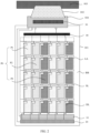
- FIG. 1 is a schematic diagram of a display apparatus according to an embodiment of this application
- FIG. 2 is a schematic diagram of another display apparatus according to an embodiment of this application.
- the display apparatus includes a display panel 001, and the display panel 001 includes a display area AA and a non-display area BB surrounding the display area AA.
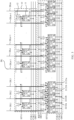
- one first signal line DL may be electrically connected to two adjacent first signal lines DL respectively by using different connection switches 12, so that two methods are available for repair of one first signal line DL, which may improve flexibility of repair.
- the signal line repair module 10 includes m/2 stages of cascaded first shift units 11: a first-stage first shift unit 111, a second-stage first shift unit 112, ..., and a (m/2) th -stage first shift unit 11(m/2); the first first signal line DL1 and the second first shift unit DL2 are electrically connected to an input end and an output end of a connection switch 12 electrically connected to the first-stage first shift unit 111 respectively, the third first signal line DL3 and the fourth first shift unit DL4 are electrically connected to an input end and an output end of a connection switch 12 electrically connected to the second-stage first shift unit 112 respectively, ..., and the (m-1) th first signal line DL(m-1) and the m th first shift unit DLm are electrically connected to an input end and an output end of a connection switch 12 electrically connected to the (m-2) th -stage first shift unit 1 1(m/2) respectively.
- m is an even number.
- every two first signal lines DL correspond to one connection switch 12 and one stage of first shift unit 11, which minimizes a quantity of first shift units 11 and makes it easy to implement a narrow frame.
- the first shift unit 11 of the stage used for repair is enabled to output an enable signal relatively quickly in the repair process, and efficiency is higher.
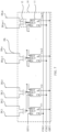
- FIG. 12 is a partial enlarged view of yet another display apparatus according to an embodiment of this application.
- at least one first signal line DL electrically connected to another connection switch 12 is disposed, that is, connection switches 12 connected to two adjacent first signal lines DL among m first signal lines DL electrically connected to the signal line repair module 10 are different.
- connection switches 12 connected to two adjacent first signal lines DL among m first signal lines DL electrically connected to the signal line repair module 10 are different.
- a non-display area BB of the display apparatus is further provided with a signal line defect detection module 20, and the signal line defect detection module 20 is electrically connected to a first signal line DL and configured to detect a defect of the first signal line DL.
- each reset switch 22b is electrically connected to the reset line REF, and an output end thereof is electrically connected to the detection line DET.
- the second shift units 21 may have the same structure and operating principle as the first shift units 11, and the second-stage shift units 21 may also be cascaded in the same manner as the first shift units 11.
- a turn-on signal input end IN of a first-stage second shift unit 21 is electrically connected to a start signal line, for example, a second start signal line STV2, and the second start signal line STV2 provides an enable signal to the turn-on signal input end IN of the first-stage second shift unit 21.
- Clock signal input ends CLK of two stages of adjacent second shift units 21 among the cascaded second shift units 21 are connected to different clock signal lines. As shown in FIG.
- signals on the first signal lines DL should be sequentially transmitted to the drive chip 3030 or a mainboard 004 by using the detection line DET, and then the first-type second shift units 21a should be sequentially turned on, so that the corresponding detection switches 22a are sequentially turned on.
- the second-type second shift units 21b should also be sequentially turned on, so that the corresponding reset switches 22b are sequentially turned on.
- the first-type second shift units 21a and the second-type second shift units 21b are sequentially and alternately disposed and cascaded, that is, the second shift units 21 in the signal line defect detection module 20 are sequentially cascaded, and the second-type second shift units 21b are disposed between adjacent first-type second shift units 21a.
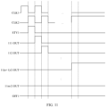
- the first-type second shift units 21a are sequentially cascaded and the second-type second shift units 21b are sequentially cascaded. Then, after one first-type second shift unit 21a outputs an enable signal, detection of one first signal line DL is completed; then the first-type second shift unit 21a is turned off and one second-type second shift unit 21b outputs an enable signal to complete resetting of the detection line DET; then the first-type second shift unit 21a cascaded with and adjacent to the previous first-type second shift unit 21a outputs an enable signal to complete detection of one first signal line DL; ...; and this operation is repeated until detection of all the first signal lines DL is completed.
- defect detection of the first signal lines DL does not require detection software or a detection device such as a microscope, which can reduce detection costs and improve detection efficiency.
- An operating stage of the display panel further includes a signal line defect detection stage.
- the signal line defect detection module 20 operates and locates a defective first signal line DL.
- the signal line repair module 10 in each foregoing embodiment may be started to complete repair of the disconnected first signal line DL.
- FIG. 14 is a schematic diagram of a structure of a drive chip according to an embodiment of this application.
- the drive chip includes a control unit 311 and an input/output unit 312.
- the control unit 311 instructs the input/output unit 312 to provide a control signal, so that the disconnected first signal line DL is electrically connected to another first signal line DL.
- a control signal is provided to a plurality of cascaded first shift units 11, to control shift output ends of the a plurality of stages of cascaded first shift units 11 to sequentially output enable signals.
- an enable signal is provided to a start signal line
- a reset signal is provided to a reset signal line
- pulse signals are provided to a clock signal line
- enable signals or disable signals are continuously output after a plurality of pulse signals are output to the clock signal line.
- the control unit 311 is also configured to instruct the input/output unit 312 to continuously output a control signal to a first shift unit 11 corresponding to a connection switch 12 electrically connected to the disconnected first signal line DL, so that the first shift unit 11 continuously outputs an enable signal in the display stage, to control the connection switch 12 electrically connected to the disconnected first signal line DL to be continuously turned on, so that the disconnected first signal line DL is electrically connected to another first signal line DL.
- enable signals or disable signals are continuously output after a plurality of pulse signals are output to clock signal lines.
- the drive chip is further configured to: when it is determined to enter a signal line defect detection stage, determine whether a to-be-detected first signal line DL is disconnected based on a result of comparison between a detection result signal obtained from a detection line DET electrically connected to the drive chip and a test signal sent to the to-be-detected first signal line DL.
- the input/output unit 312 provides a test signal to a first signal line DL, so that the test signal is transmitted on the first signal line DL, and the test signal is used as a reference value for detecting whether the first signal line DL is defective;
- the control unit 311 is further configured to compare a signal on the detection line DET with a test signal after receiving the signal that is on the detection line DET and that is transmitted by the input/output unit 312, and determine that a first signal line DL corresponding to the signal is defective when the signal on the detection line DET is different from the test signal.
- the control unit 311 instructs the input/output unit 312 to output corresponding signals in the signal line repair stage and the display stage based on the position of the defective first signal line DL.
- the drive chip further provides a signal to a plurality of first signal lines DL to control sub-pixels P0 to perform light-emitting display.
- the drive chip in FIG. 1 or FIG. 2 is the drive chip 30 according to this embodiment of FIG. 14 of this application.
- FIG. 15 is a schematic diagram of an electronic device according to an embodiment of this application.
- the electronic device includes the display apparatus according to any one of the embodiments of this application.
- the specific structure of the display apparatus has been described in detail in the foregoing embodiments. Details are not described herein again.
- the electronic device shown in FIG. 15 is provided only for schematic illustration, and may be, for example, any electronic device with a display function, such as a mobile phone, a tablet computer, a notebook computer, an E-book reader, a TV, or a smartwatch.
Landscapes
- Engineering & Computer Science (AREA)
- Physics & Mathematics (AREA)
- Computer Hardware Design (AREA)
- General Physics & Mathematics (AREA)
- Theoretical Computer Science (AREA)
- Control Of Indicators Other Than Cathode Ray Tubes (AREA)
Claims (12)
- Appareil d'affichage, comprenant :une pluralité de sous-pixels (P0), dans lequel les sous-pixels sont utilisés pour un affichage électroluminescent ;une pluralité de lignes de signal (DL, SL), dans lequel la pluralité de lignes de signal sont connectées électriquement à la pluralité de sous-pixels et fournissent un signal requis pour un affichage électroluminescent à la pluralité de sous-pixels ;un module de réparation de ligne de signal (10), dans lequel le module de réparation de ligne de signal est connecté électriquement à la pluralité de lignes de signal, et configuré pour réparer une ligne de signal déconnectée ; et le module de réparation de ligne de signal comprend :une pluralité de commutateurs de connexion (12), dans lequel une extrémité d'entrée de chaque commutateur de connexion est connectée électriquement à une ligne de signal, et une extrémité de sortie de celui-ci est connectée électriquement à une autre ligne de signal ;une pluralité de premières unités de décalage (11), dans lequel la pluralité de premières unités de décalage sont en cascade séquentielle, et la pluralité de premières unités de décalage sont disposées dans une correspondance biunivoque avec la pluralité de commutateurs de connexion ; et une extrémité de sortie de décalage de chaque première unité de décalage est connectée électriquement à une extrémité de commande d'un commutateur de connexion correspondant ; etune puce d'attaque (30), dans laquelle la puce d'attaque est connectée électriquement à la pluralité de lignes de signal et au module de réparation de ligne de signal, et est configurée pour fournir le signal requis pour commander l'affichage d'émission de lumière des sous-pixels aux lignes de signal, envoyer, lors de la détermination qu'une ligne de signal déconnectée existe, un signal de commande au module de réparation de ligne de signal pour permettre à des extrémités de sortie de décalage de la pluralité de premières unités de décalage de délivrer séquentiellement des signaux d'activation, et permettre à la première unité de décalage correspondant à un commutateur de connexion connecté électriquement à la ligne de signal déconnecté de délivrer en sortie en continu des signaux d'activation, pour commander le commutateur de connexion connecté électriquement à la ligne de signal déconnectée pour être activé en continu, de sorte que la ligne de signal déconnectée est électriquement connectée à une autre ligne de signal.
- Appareil d'affichage selon la revendication 1, dans lequel toutes deux lignes de signal adjacentes parmi la pluralité de lignes de signal connectées électriquement au module de réparation de ligne de signal (10) sont connectées électriquement à l'extrémité d'entrée et à l'extrémité de sortie d'un même commutateur de connexion respectivement.
- Appareil d'affichage selon la revendication 1 ou 2, dans lequel toutes les deux lignes de signal adjacentes parmi la pluralité de lignes de signal connectées électriquement au module de réparation de ligne de signal (10) sont connectées électriquement à l'extrémité d'entrée et à l'extrémité de sortie d'un même commutateur de connexion respectivement.
- Appareil d'affichage selon l'une quelconque des revendications 1 à 3, dans lequel entre deux lignes de signal connectées électriquement à un même commutateur de connexion (12), au moins une ligne de signal connectée électriquement à un autre commutateur de connexion est comprise.
- Appareil d'affichage selon la revendication 4, dans lequel la pluralité de sous-pixels comprend au moins des sous-pixels avec trois couleurs d'émission de lumière, des sous-pixels dans une même colonne ayant une même couleur d'émission de lumière, et une ligne de signal fournit un signal aux sous-pixels dans la même colonne ; et
une ligne de signal connectée électriquement à l'extrémité d'entrée de chaque commutateur de connexion et une ligne de signal connectée électriquement à l'extrémité de sortie du commutateur de connexion (12) fournit des signaux à des sous-pixels d'une même couleur d'émission de lumière située dans des colonnes différentes, respectivement. - Appareil d'affichage selon l'une quelconque des revendications 1 à 5, dans lequel la zone de non-affichage (BB) comprend en outre un module de détection de défaut de ligne de signal (200), le module de détection de défaut de ligne de signal est connecté électriquement aux lignes de signal et configuré pour détecter un défaut des lignes de signal, et le module de détection de ligne de signal comprend :une ligne de détection (DET), configurée pour transmettre des signaux sur les lignes de signal à la puce d'attaque ;une ligne de réinitialisation (REF), configurée pour obtenir un signal de réinitialisation à partir de la puce d'attaque et transmettre le signal de réinitialisation à la ligne de détection ;une pluralité de commutateurs de détection (22a), dans lequel la pluralité de commutateurs de détection sont disposés dans une correspondance biunivoque avec une pluralité de lignes de signal, une extrémité d'entrée de chaque commutateur de détection est connectée électriquement à une ligne de signal, une extrémité de sortie de celle-ci est connectée électriquement à la ligne de détection, et lorsque le commutateur de détection est activé, un signal sur la ligne de signal connecté électriquement à l'extrémité d'entrée du commutateur de détection est transmis à la ligne de détection connectée électriquement à l'extrémité de sortie du commutateur de détection ; etdes commutateurs de réinitialisation (22b), dans lequel une extrémité d'entrée de chaque commutateur de réinitialisation est connectée électriquement à la ligne de réparation, et une extrémité de sortie de celui-ci est connectée électriquement à la ligne de détection ; et lorsque le commutateur de réinitialisation est allumé, un signal de réinitialisation transmis sur la ligne de réinitialisation connectée électriquement à l'extrémité d'entrée du commutateur de réinitialisation est transmis à la ligne de détection.
- Appareil d'affichage selon la revendication 6, dans lequel le module de détection de défaut de ligne de signal (200) comprend une pluralité de commutateurs de réinitialisation, les commutateurs de détection et les commutateurs de réinitialisation sont disposés en alternance dans une correspondance biunivoque, et les commutateurs de réinitialisation sont allumés après que les commutateurs de détection correspondants sont allumés puis éteints.
- Appareil d'affichage selon la revendication 7, dans lequel le module de détection de ligne de signal comprend en outre une pluralité de secondes unités de décalage, et la pluralité de seconds décalage comprend une pluralité de secondes unités de décalage de premier type et une pluralité de secondes unités de décalage de second type ;une pluralité de secondes unités de décalage de premier type sont connectées électriquement aux commutateurs de détection dans une correspondance biunivoque, et des signaux délivrés en sortie par les extrémités de sortie de décalage des secondes unités de décalage de premier type commandent l'allumage ou l'extinction des commutateurs de détection connectés électriquement à celles-ci ; etune pluralité de secondes unités de décalage de second type sont connectées électriquement aux commutateurs de réinitialisation dans une correspondance biunivoque, et des signaux délivrés en sortie par les extrémités de sortie de décalage des secondes unités de décalage de second type commandent l'allumage ou l'extinction des commutateurs de réinitialisation connectés électriquement à celles-ci ;
- Appareil d'affichage selon la revendication 8, dans lequel les secondes unités de décalage de second type et les secondes unités de décalage de second type sont disposées séquentiellement et alternativement en cascade.
- Appareil d'affichage selon la revendication 8, dans lequel la pluralité de secondes unités de décalage de premier type sont en cascade séquentielle, et les secondes unités de décalage de second type sont en cascade séquentielle.
- Appareil d'affichage selon l'une quelconque des revendications précédentes, dans lequel la puce d'attaque (30) est configurée pour :
dans un étage de détection de défaut de ligne de signal, déterminer si une ligne de signal à détecter est déconnectée sur la base d'un résultat de comparaison entre un signal de résultat de détection obtenu à partir d'une ligne de détection connectée électriquement à la puce d'attaque et un signal de test envoyé à la ligne de signal à détecter. - Dispositif électronique, comprenant l'appareil d'affichage selon l'une quelconque des revendications 1 à 11.
Applications Claiming Priority (2)
| Application Number | Priority Date | Filing Date | Title |
|---|---|---|---|
| CN202011066174.XA CN114360439B (zh) | 2020-09-30 | 2020-09-30 | 一种显示装置、驱动芯片及电子设备 |
| PCT/CN2021/119662 WO2022068655A1 (fr) | 2020-09-30 | 2021-09-22 | Dispositif d'affichage, puce d'attaque et dispositif électronique |
Publications (3)
| Publication Number | Publication Date |
|---|---|
| EP4083989A1 EP4083989A1 (fr) | 2022-11-02 |
| EP4083989A4 EP4083989A4 (fr) | 2023-08-09 |
| EP4083989B1 true EP4083989B1 (fr) | 2024-07-10 |
Family
ID=80949702
Family Applications (1)
| Application Number | Title | Priority Date | Filing Date |
|---|---|---|---|
| EP21874316.9A Active EP4083989B1 (fr) | 2020-09-30 | 2021-09-22 | Dispositif d'affichage, puce d'attaque et dispositif électronique |
Country Status (4)
| Country | Link |
|---|---|
| US (1) | US11928996B2 (fr) |
| EP (1) | EP4083989B1 (fr) |
| CN (1) | CN114360439B (fr) |
| WO (1) | WO2022068655A1 (fr) |
Families Citing this family (3)
| Publication number | Priority date | Publication date | Assignee | Title |
|---|---|---|---|---|
| CN114333580B (zh) * | 2021-12-21 | 2022-11-25 | Tcl华星光电技术有限公司 | 显示面板及显示装置 |
| CN115148138A (zh) * | 2022-08-12 | 2022-10-04 | 乐金显示光电科技(中国)有限公司 | 修复设备 |
| TWI908567B (zh) * | 2024-12-27 | 2025-12-11 | 虹彩光電股份有限公司 | 顯示裝置及顯示裝置檢測方法 |
Family Cites Families (18)
| Publication number | Priority date | Publication date | Assignee | Title |
|---|---|---|---|---|
| JP3136066B2 (ja) * | 1994-12-28 | 2001-02-19 | シャープ株式会社 | 液晶表示装置 |
| US6816143B1 (en) * | 1999-11-23 | 2004-11-09 | Koninklijke Philips Electronics N.V. | Self diagnostic and repair in matrix display panel |
| CN100365494C (zh) * | 2004-12-20 | 2008-01-30 | 凌阳科技股份有限公司 | 具修复断线功能的薄膜晶体管液晶显示器及高阻抗侦测电路 |
| TWI319104B (en) | 2005-09-20 | 2010-01-01 | Chi Mei Optoelectronics Corp | Apparatus for driving a flat panel display and repair flat panel display signal line |
| TWI336003B (en) * | 2005-11-14 | 2011-01-11 | Au Optronics Corp | Liquid crystal apparatus and repair lines structure thereof |
| CN106205519B (zh) * | 2011-04-08 | 2018-11-20 | 夏普株式会社 | 显示装置和显示装置的驱动方法 |
| KR101910080B1 (ko) * | 2011-12-08 | 2018-12-20 | 삼성디스플레이 주식회사 | 주사 구동 회로 및 이의 리페어 방법 |
| CN102879964B (zh) * | 2012-10-11 | 2015-04-29 | 深圳市华星光电技术有限公司 | 一种阵列基板及psva型液晶显示面板 |
| CN103680370A (zh) | 2013-12-17 | 2014-03-26 | 深圳市华星光电技术有限公司 | 显示装置及其测试线路修复方法 |
| JP6370057B2 (ja) | 2014-02-20 | 2018-08-08 | 三菱電機株式会社 | アレイ基板およびアレイ基板の検査方法 |
| KR20160065263A (ko) * | 2014-11-28 | 2016-06-09 | 삼성디스플레이 주식회사 | 멀티-타임 프로그래머블 동작의 수행 방법 및 이를 채용한 유기 발광 표시 장치 |
| CN105448265B (zh) * | 2016-01-04 | 2018-02-13 | 京东方科技集团股份有限公司 | 一种修复单元及其修复方法、栅极驱动电路、显示装置 |
| CN105575305B (zh) | 2016-03-17 | 2018-10-30 | 京东方科技集团股份有限公司 | 一种信号线断线修复电路、方法和显示面板 |
| CN112384969B (zh) * | 2018-07-13 | 2023-09-12 | 堺显示器制品株式会社 | 显示装置 |
| US11043165B2 (en) * | 2019-04-29 | 2021-06-22 | Wuhan China Star Optoelectronics Semiconductor Display Technology Co., Ltd. | Active-matrix organic light emitting diode (AMOLED) panel cell testing circuit and method for repairing data lines via same |
| CN109949729A (zh) | 2019-04-29 | 2019-06-28 | 武汉华星光电半导体显示技术有限公司 | Amoled面板成盒检测电路及其修复数据线的方法 |
| CN110806667B (zh) * | 2019-11-05 | 2021-12-14 | 昆山龙腾光电股份有限公司 | 显示面板、显示面板的数据线的修复方法和液晶显示装置 |
| CN211603773U (zh) * | 2020-01-08 | 2020-09-29 | 昆山龙腾光电股份有限公司 | 一种液晶显示器 |
-
2020
- 2020-09-30 CN CN202011066174.XA patent/CN114360439B/zh active Active
-
2021
- 2021-09-22 US US17/793,520 patent/US11928996B2/en active Active
- 2021-09-22 WO PCT/CN2021/119662 patent/WO2022068655A1/fr not_active Ceased
- 2021-09-22 EP EP21874316.9A patent/EP4083989B1/fr active Active
Also Published As
| Publication number | Publication date |
|---|---|
| EP4083989A1 (fr) | 2022-11-02 |
| US20230119866A1 (en) | 2023-04-20 |
| US11928996B2 (en) | 2024-03-12 |
| CN114360439A (zh) | 2022-04-15 |
| WO2022068655A1 (fr) | 2022-04-07 |
| CN114360439B (zh) | 2022-12-20 |
| EP4083989A4 (fr) | 2023-08-09 |
Similar Documents
| Publication | Publication Date | Title |
|---|---|---|
| EP4083988B1 (fr) | Appareil d'affichage, puce d'attaque et dispositif électronique | |
| US11935498B2 (en) | Display apparatus with signal repair circuit, drive chip therefor, and related electronic device | |
| CN110178174B (zh) | 一种栅极驱动电路及其控制方法、移动终端 | |
| EP4083989B1 (fr) | Dispositif d'affichage, puce d'attaque et dispositif électronique | |
| US11398172B2 (en) | Display panel and manufacturing method thereof, and display device | |
| CN111881847B (zh) | 显示面板及其检测方法、显示装置 | |
| US20200035148A1 (en) | Pixel circuit and driving method thereof, display panel and video wall | |
| EP3716259B1 (fr) | Dispositif d'affichage, dispositif électronique à mosaïque et procédé de réparation d'un dispositif d'affichage | |
| US20240045530A1 (en) | Detection method, display panel, driver chip and display device | |
| US20200027404A1 (en) | Display panel, method for driving the same, and display device | |
| US11900868B2 (en) | Display panel and display device | |
| WO2021143824A1 (fr) | Substrat d'affichage et son procédé de détection, et appareil d'affichage | |
| US12211440B2 (en) | Starting signal providing module, method and splicing display device | |
| US20170160843A1 (en) | Display panel, driving method, and display device | |
| CN114255680B (zh) | 显示装置及其检测方法、存储介质、显示驱动芯片和设备 | |
| CN113920946A (zh) | 栅极驱动器及其驱动方法、显示装置 | |
| CN115132129A (zh) | 驱动电路、显示模组及显示装置 | |
| KR20250083085A (ko) | 디스플레이 패널, 이의 테스트 방법 및 디스플레이 장치 | |
| US12482403B2 (en) | Power-supply adjusting circuit and display terminal | |
| US8542173B2 (en) | Display panel and driving method thereof | |
| HK40069178A (en) | Display apparatus, driving chip, and electronic device | |
| HK40069178B (en) | Display apparatus, driving chip, and electronic device | |
| HK40069182A (en) | Display apparatus, driving chip, and electronic device | |
| HK40069182B (en) | Display apparatus, driving chip, and electronic device | |
| US20250225941A1 (en) | Display driver, display panel, and image display driving method |
Legal Events
| Date | Code | Title | Description |
|---|---|---|---|
| STAA | Information on the status of an ep patent application or granted ep patent |
Free format text: STATUS: THE INTERNATIONAL PUBLICATION HAS BEEN MADE |
|
| PUAI | Public reference made under article 153(3) epc to a published international application that has entered the european phase |
Free format text: ORIGINAL CODE: 0009012 |
|
| STAA | Information on the status of an ep patent application or granted ep patent |
Free format text: STATUS: REQUEST FOR EXAMINATION WAS MADE |
|
| 17P | Request for examination filed |
Effective date: 20220725 |
|
| AK | Designated contracting states |
Kind code of ref document: A1 Designated state(s): AL AT BE BG CH CY CZ DE DK EE ES FI FR GB GR HR HU IE IS IT LI LT LU LV MC MK MT NL NO PL PT RO RS SE SI SK SM TR |
|
| REG | Reference to a national code |
Ref country code: DE Ref legal event code: R079 Free format text: PREVIOUS MAIN CLASS: G09G0003320000 Ipc: G09G0003200000 Ref country code: DE Ref legal event code: R079 Ref document number: 602021015639 Country of ref document: DE Free format text: PREVIOUS MAIN CLASS: G09G0003320000 Ipc: G09G0003200000 |
|
| A4 | Supplementary search report drawn up and despatched |
Effective date: 20230706 |
|
| RIC1 | Information provided on ipc code assigned before grant |
Ipc: G09G 3/32 20160101ALI20230630BHEP Ipc: G09G 3/00 20060101ALI20230630BHEP Ipc: G09G 3/20 20060101AFI20230630BHEP |
|
| DAV | Request for validation of the european patent (deleted) | ||
| DAX | Request for extension of the european patent (deleted) | ||
| GRAP | Despatch of communication of intention to grant a patent |
Free format text: ORIGINAL CODE: EPIDOSNIGR1 |
|
| STAA | Information on the status of an ep patent application or granted ep patent |
Free format text: STATUS: GRANT OF PATENT IS INTENDED |
|
| RIC1 | Information provided on ipc code assigned before grant |
Ipc: G09G 3/32 20160101ALI20240102BHEP Ipc: G09G 3/00 20060101ALI20240102BHEP Ipc: G09G 3/20 20060101AFI20240102BHEP |
|
| INTG | Intention to grant announced |
Effective date: 20240206 |
|
| GRAS | Grant fee paid |
Free format text: ORIGINAL CODE: EPIDOSNIGR3 |
|
| GRAA | (expected) grant |
Free format text: ORIGINAL CODE: 0009210 |
|
| STAA | Information on the status of an ep patent application or granted ep patent |
Free format text: STATUS: THE PATENT HAS BEEN GRANTED |
|
| AK | Designated contracting states |
Kind code of ref document: B1 Designated state(s): AL AT BE BG CH CY CZ DE DK EE ES FI FR GB GR HR HU IE IS IT LI LT LU LV MC MK MT NL NO PL PT RO RS SE SI SK SM TR |
|
| REG | Reference to a national code |
Ref country code: CH Ref legal event code: EP |
|
| REG | Reference to a national code |
Ref country code: DE Ref legal event code: R096 Ref document number: 602021015639 Country of ref document: DE |
|
| REG | Reference to a national code |
Ref country code: NL Ref legal event code: FP |
|
| REG | Reference to a national code |
Ref country code: LT Ref legal event code: MG9D |
|
| PG25 | Lapsed in a contracting state [announced via postgrant information from national office to epo] |
Ref country code: PT Free format text: LAPSE BECAUSE OF FAILURE TO SUBMIT A TRANSLATION OF THE DESCRIPTION OR TO PAY THE FEE WITHIN THE PRESCRIBED TIME-LIMIT Effective date: 20241111 |
|
| REG | Reference to a national code |
Ref country code: AT Ref legal event code: MK05 Ref document number: 1702755 Country of ref document: AT Kind code of ref document: T Effective date: 20240710 |
|
| PG25 | Lapsed in a contracting state [announced via postgrant information from national office to epo] |
Ref country code: PT Free format text: LAPSE BECAUSE OF FAILURE TO SUBMIT A TRANSLATION OF THE DESCRIPTION OR TO PAY THE FEE WITHIN THE PRESCRIBED TIME-LIMIT Effective date: 20241111 |
|
| PG25 | Lapsed in a contracting state [announced via postgrant information from national office to epo] |
Ref country code: NO Free format text: LAPSE BECAUSE OF FAILURE TO SUBMIT A TRANSLATION OF THE DESCRIPTION OR TO PAY THE FEE WITHIN THE PRESCRIBED TIME-LIMIT Effective date: 20241010 |
|
| PG25 | Lapsed in a contracting state [announced via postgrant information from national office to epo] |
Ref country code: FI Free format text: LAPSE BECAUSE OF FAILURE TO SUBMIT A TRANSLATION OF THE DESCRIPTION OR TO PAY THE FEE WITHIN THE PRESCRIBED TIME-LIMIT Effective date: 20240710 Ref country code: PL Free format text: LAPSE BECAUSE OF FAILURE TO SUBMIT A TRANSLATION OF THE DESCRIPTION OR TO PAY THE FEE WITHIN THE PRESCRIBED TIME-LIMIT Effective date: 20240710 Ref country code: GR Free format text: LAPSE BECAUSE OF FAILURE TO SUBMIT A TRANSLATION OF THE DESCRIPTION OR TO PAY THE FEE WITHIN THE PRESCRIBED TIME-LIMIT Effective date: 20241011 |
|
| PG25 | Lapsed in a contracting state [announced via postgrant information from national office to epo] |
Ref country code: BG Free format text: LAPSE BECAUSE OF FAILURE TO SUBMIT A TRANSLATION OF THE DESCRIPTION OR TO PAY THE FEE WITHIN THE PRESCRIBED TIME-LIMIT Effective date: 20240710 |
|
| PG25 | Lapsed in a contracting state [announced via postgrant information from national office to epo] |
Ref country code: LV Free format text: LAPSE BECAUSE OF FAILURE TO SUBMIT A TRANSLATION OF THE DESCRIPTION OR TO PAY THE FEE WITHIN THE PRESCRIBED TIME-LIMIT Effective date: 20240710 |
|
| PG25 | Lapsed in a contracting state [announced via postgrant information from national office to epo] |
Ref country code: IS Free format text: LAPSE BECAUSE OF FAILURE TO SUBMIT A TRANSLATION OF THE DESCRIPTION OR TO PAY THE FEE WITHIN THE PRESCRIBED TIME-LIMIT Effective date: 20241110 Ref country code: AT Free format text: LAPSE BECAUSE OF FAILURE TO SUBMIT A TRANSLATION OF THE DESCRIPTION OR TO PAY THE FEE WITHIN THE PRESCRIBED TIME-LIMIT Effective date: 20240710 |
|
| PG25 | Lapsed in a contracting state [announced via postgrant information from national office to epo] |
Ref country code: HR Free format text: LAPSE BECAUSE OF FAILURE TO SUBMIT A TRANSLATION OF THE DESCRIPTION OR TO PAY THE FEE WITHIN THE PRESCRIBED TIME-LIMIT Effective date: 20240710 |
|
| PG25 | Lapsed in a contracting state [announced via postgrant information from national office to epo] |
Ref country code: RS Free format text: LAPSE BECAUSE OF FAILURE TO SUBMIT A TRANSLATION OF THE DESCRIPTION OR TO PAY THE FEE WITHIN THE PRESCRIBED TIME-LIMIT Effective date: 20241010 Ref country code: ES Free format text: LAPSE BECAUSE OF FAILURE TO SUBMIT A TRANSLATION OF THE DESCRIPTION OR TO PAY THE FEE WITHIN THE PRESCRIBED TIME-LIMIT Effective date: 20240710 |
|
| PG25 | Lapsed in a contracting state [announced via postgrant information from national office to epo] |
Ref country code: RS Free format text: LAPSE BECAUSE OF FAILURE TO SUBMIT A TRANSLATION OF THE DESCRIPTION OR TO PAY THE FEE WITHIN THE PRESCRIBED TIME-LIMIT Effective date: 20241010 Ref country code: PL Free format text: LAPSE BECAUSE OF FAILURE TO SUBMIT A TRANSLATION OF THE DESCRIPTION OR TO PAY THE FEE WITHIN THE PRESCRIBED TIME-LIMIT Effective date: 20240710 Ref country code: NO Free format text: LAPSE BECAUSE OF FAILURE TO SUBMIT A TRANSLATION OF THE DESCRIPTION OR TO PAY THE FEE WITHIN THE PRESCRIBED TIME-LIMIT Effective date: 20241010 Ref country code: LV Free format text: LAPSE BECAUSE OF FAILURE TO SUBMIT A TRANSLATION OF THE DESCRIPTION OR TO PAY THE FEE WITHIN THE PRESCRIBED TIME-LIMIT Effective date: 20240710 Ref country code: IS Free format text: LAPSE BECAUSE OF FAILURE TO SUBMIT A TRANSLATION OF THE DESCRIPTION OR TO PAY THE FEE WITHIN THE PRESCRIBED TIME-LIMIT Effective date: 20241110 Ref country code: HR Free format text: LAPSE BECAUSE OF FAILURE TO SUBMIT A TRANSLATION OF THE DESCRIPTION OR TO PAY THE FEE WITHIN THE PRESCRIBED TIME-LIMIT Effective date: 20240710 Ref country code: GR Free format text: LAPSE BECAUSE OF FAILURE TO SUBMIT A TRANSLATION OF THE DESCRIPTION OR TO PAY THE FEE WITHIN THE PRESCRIBED TIME-LIMIT Effective date: 20241011 Ref country code: FI Free format text: LAPSE BECAUSE OF FAILURE TO SUBMIT A TRANSLATION OF THE DESCRIPTION OR TO PAY THE FEE WITHIN THE PRESCRIBED TIME-LIMIT Effective date: 20240710 Ref country code: ES Free format text: LAPSE BECAUSE OF FAILURE TO SUBMIT A TRANSLATION OF THE DESCRIPTION OR TO PAY THE FEE WITHIN THE PRESCRIBED TIME-LIMIT Effective date: 20240710 Ref country code: BG Free format text: LAPSE BECAUSE OF FAILURE TO SUBMIT A TRANSLATION OF THE DESCRIPTION OR TO PAY THE FEE WITHIN THE PRESCRIBED TIME-LIMIT Effective date: 20240710 Ref country code: AT Free format text: LAPSE BECAUSE OF FAILURE TO SUBMIT A TRANSLATION OF THE DESCRIPTION OR TO PAY THE FEE WITHIN THE PRESCRIBED TIME-LIMIT Effective date: 20240710 |
|
| REG | Reference to a national code |
Ref country code: DE Ref legal event code: R097 Ref document number: 602021015639 Country of ref document: DE |
|
| PG25 | Lapsed in a contracting state [announced via postgrant information from national office to epo] |
Ref country code: SM Free format text: LAPSE BECAUSE OF FAILURE TO SUBMIT A TRANSLATION OF THE DESCRIPTION OR TO PAY THE FEE WITHIN THE PRESCRIBED TIME-LIMIT Effective date: 20240710 Ref country code: RO Free format text: LAPSE BECAUSE OF FAILURE TO SUBMIT A TRANSLATION OF THE DESCRIPTION OR TO PAY THE FEE WITHIN THE PRESCRIBED TIME-LIMIT Effective date: 20240710 Ref country code: DK Free format text: LAPSE BECAUSE OF FAILURE TO SUBMIT A TRANSLATION OF THE DESCRIPTION OR TO PAY THE FEE WITHIN THE PRESCRIBED TIME-LIMIT Effective date: 20240710 |
|
| PG25 | Lapsed in a contracting state [announced via postgrant information from national office to epo] |
Ref country code: MC Free format text: LAPSE BECAUSE OF FAILURE TO SUBMIT A TRANSLATION OF THE DESCRIPTION OR TO PAY THE FEE WITHIN THE PRESCRIBED TIME-LIMIT Effective date: 20240710 Ref country code: EE Free format text: LAPSE BECAUSE OF FAILURE TO SUBMIT A TRANSLATION OF THE DESCRIPTION OR TO PAY THE FEE WITHIN THE PRESCRIBED TIME-LIMIT Effective date: 20240710 |
|
| PG25 | Lapsed in a contracting state [announced via postgrant information from national office to epo] |
Ref country code: CZ Free format text: LAPSE BECAUSE OF FAILURE TO SUBMIT A TRANSLATION OF THE DESCRIPTION OR TO PAY THE FEE WITHIN THE PRESCRIBED TIME-LIMIT Effective date: 20240710 |
|
| PG25 | Lapsed in a contracting state [announced via postgrant information from national office to epo] |
Ref country code: IT Free format text: LAPSE BECAUSE OF FAILURE TO SUBMIT A TRANSLATION OF THE DESCRIPTION OR TO PAY THE FEE WITHIN THE PRESCRIBED TIME-LIMIT Effective date: 20240710 Ref country code: SK Free format text: LAPSE BECAUSE OF FAILURE TO SUBMIT A TRANSLATION OF THE DESCRIPTION OR TO PAY THE FEE WITHIN THE PRESCRIBED TIME-LIMIT Effective date: 20240710 |
|
| REG | Reference to a national code |
Ref country code: CH Ref legal event code: PL |
|
| PLBE | No opposition filed within time limit |
Free format text: ORIGINAL CODE: 0009261 |
|
| STAA | Information on the status of an ep patent application or granted ep patent |
Free format text: STATUS: NO OPPOSITION FILED WITHIN TIME LIMIT |
|
| PG25 | Lapsed in a contracting state [announced via postgrant information from national office to epo] |
Ref country code: LU Free format text: LAPSE BECAUSE OF NON-PAYMENT OF DUE FEES Effective date: 20240922 |
|
| 26N | No opposition filed |
Effective date: 20250411 |
|
| REG | Reference to a national code |
Ref country code: BE Ref legal event code: MM Effective date: 20240930 |
|
| PG25 | Lapsed in a contracting state [announced via postgrant information from national office to epo] |
Ref country code: BE Free format text: LAPSE BECAUSE OF NON-PAYMENT OF DUE FEES Effective date: 20240930 |
|
| PG25 | Lapsed in a contracting state [announced via postgrant information from national office to epo] |
Ref country code: FR Free format text: LAPSE BECAUSE OF NON-PAYMENT OF DUE FEES Effective date: 20240930 |
|
| PG25 | Lapsed in a contracting state [announced via postgrant information from national office to epo] |
Ref country code: CH Free format text: LAPSE BECAUSE OF NON-PAYMENT OF DUE FEES Effective date: 20240930 |
|
| PG25 | Lapsed in a contracting state [announced via postgrant information from national office to epo] |
Ref country code: IE Free format text: LAPSE BECAUSE OF NON-PAYMENT OF DUE FEES Effective date: 20240922 |
|
| PG25 | Lapsed in a contracting state [announced via postgrant information from national office to epo] |
Ref country code: SE Free format text: LAPSE BECAUSE OF FAILURE TO SUBMIT A TRANSLATION OF THE DESCRIPTION OR TO PAY THE FEE WITHIN THE PRESCRIBED TIME-LIMIT Effective date: 20240710 |
|
| PGFP | Annual fee paid to national office [announced via postgrant information from national office to epo] |
Ref country code: NL Payment date: 20250814 Year of fee payment: 5 |
|
| PGFP | Annual fee paid to national office [announced via postgrant information from national office to epo] |
Ref country code: DE Payment date: 20250730 Year of fee payment: 5 |
|
| PGFP | Annual fee paid to national office [announced via postgrant information from national office to epo] |
Ref country code: GB Payment date: 20250731 Year of fee payment: 5 |
|
| PG25 | Lapsed in a contracting state [announced via postgrant information from national office to epo] |
Ref country code: CY Free format text: LAPSE BECAUSE OF FAILURE TO SUBMIT A TRANSLATION OF THE DESCRIPTION OR TO PAY THE FEE WITHIN THE PRESCRIBED TIME-LIMIT; INVALID AB INITIO Effective date: 20210922 |
|
| PG25 | Lapsed in a contracting state [announced via postgrant information from national office to epo] |
Ref country code: HU Free format text: LAPSE BECAUSE OF FAILURE TO SUBMIT A TRANSLATION OF THE DESCRIPTION OR TO PAY THE FEE WITHIN THE PRESCRIBED TIME-LIMIT; INVALID AB INITIO Effective date: 20210922 |