EP4084079A1 - Led-anzeigevorrichtung - Google Patents
Led-anzeigevorrichtung Download PDFInfo
- Publication number
- EP4084079A1 EP4084079A1 EP20907800.5A EP20907800A EP4084079A1 EP 4084079 A1 EP4084079 A1 EP 4084079A1 EP 20907800 A EP20907800 A EP 20907800A EP 4084079 A1 EP4084079 A1 EP 4084079A1
- Authority
- EP
- European Patent Office
- Prior art keywords
- led
- type electrode
- electrode
- display device
- disposed
- Prior art date
- Legal status (The legal status is an assumption and is not a legal conclusion. Google has not performed a legal analysis and makes no representation as to the accuracy of the status listed.)
- Pending
Links
Images

Classifications
-
- H—ELECTRICITY
- H10—SEMICONDUCTOR DEVICES; ELECTRIC SOLID-STATE DEVICES NOT OTHERWISE PROVIDED FOR
- H10H—INORGANIC LIGHT-EMITTING SEMICONDUCTOR DEVICES HAVING POTENTIAL BARRIERS
- H10H20/00—Individual inorganic light-emitting semiconductor devices having potential barriers, e.g. light-emitting diodes [LED]
- H10H20/01—Manufacture or treatment
-
- H—ELECTRICITY
- H10—SEMICONDUCTOR DEVICES; ELECTRIC SOLID-STATE DEVICES NOT OTHERWISE PROVIDED FOR
- H10H—INORGANIC LIGHT-EMITTING SEMICONDUCTOR DEVICES HAVING POTENTIAL BARRIERS
- H10H29/00—Integrated devices, or assemblies of multiple devices, comprising at least one light-emitting semiconductor element covered by group H10H20/00
- H10H29/10—Integrated devices comprising at least one light-emitting semiconductor component covered by group H10H20/00
- H10H29/14—Integrated devices comprising at least one light-emitting semiconductor component covered by group H10H20/00 comprising multiple light-emitting semiconductor components
- H10H29/142—Two-dimensional arrangements, e.g. asymmetric LED layout
-
- H—ELECTRICITY
- H10—SEMICONDUCTOR DEVICES; ELECTRIC SOLID-STATE DEVICES NOT OTHERWISE PROVIDED FOR
- H10D—INORGANIC ELECTRIC SEMICONDUCTOR DEVICES
- H10D86/00—Integrated devices formed in or on insulating or conducting substrates, e.g. formed in silicon-on-insulator [SOI] substrates or on stainless steel or glass substrates
- H10D86/40—Integrated devices formed in or on insulating or conducting substrates, e.g. formed in silicon-on-insulator [SOI] substrates or on stainless steel or glass substrates characterised by multiple TFTs
-
- H—ELECTRICITY
- H10—SEMICONDUCTOR DEVICES; ELECTRIC SOLID-STATE DEVICES NOT OTHERWISE PROVIDED FOR
- H10H—INORGANIC LIGHT-EMITTING SEMICONDUCTOR DEVICES HAVING POTENTIAL BARRIERS
- H10H20/00—Individual inorganic light-emitting semiconductor devices having potential barriers, e.g. light-emitting diodes [LED]
- H10H20/80—Constructional details
- H10H20/84—Coatings, e.g. passivation layers or antireflective coatings
- H10H20/841—Reflective coatings, e.g. dielectric Bragg reflectors
-
- H—ELECTRICITY
- H10—SEMICONDUCTOR DEVICES; ELECTRIC SOLID-STATE DEVICES NOT OTHERWISE PROVIDED FOR
- H10H—INORGANIC LIGHT-EMITTING SEMICONDUCTOR DEVICES HAVING POTENTIAL BARRIERS
- H10H20/00—Individual inorganic light-emitting semiconductor devices having potential barriers, e.g. light-emitting diodes [LED]
- H10H20/80—Constructional details
- H10H20/85—Packages
- H10H20/855—Optical field-shaping means, e.g. lenses
- H10H20/856—Reflecting means
-
- H—ELECTRICITY
- H10—SEMICONDUCTOR DEVICES; ELECTRIC SOLID-STATE DEVICES NOT OTHERWISE PROVIDED FOR
- H10H—INORGANIC LIGHT-EMITTING SEMICONDUCTOR DEVICES HAVING POTENTIAL BARRIERS
- H10H20/00—Individual inorganic light-emitting semiconductor devices having potential barriers, e.g. light-emitting diodes [LED]
- H10H20/80—Constructional details
- H10H20/85—Packages
- H10H20/857—Interconnections, e.g. lead-frames, bond wires or solder balls
-
- H—ELECTRICITY
- H10—SEMICONDUCTOR DEVICES; ELECTRIC SOLID-STATE DEVICES NOT OTHERWISE PROVIDED FOR
- H10W—GENERIC PACKAGES, INTERCONNECTIONS, CONNECTORS OR OTHER CONSTRUCTIONAL DETAILS OF DEVICES COVERED BY CLASS H10
- H10W90/00—Package configurations
-
- H—ELECTRICITY
- H10—SEMICONDUCTOR DEVICES; ELECTRIC SOLID-STATE DEVICES NOT OTHERWISE PROVIDED FOR
- H10D—INORGANIC ELECTRIC SEMICONDUCTOR DEVICES
- H10D86/00—Integrated devices formed in or on insulating or conducting substrates, e.g. formed in silicon-on-insulator [SOI] substrates or on stainless steel or glass substrates
- H10D86/40—Integrated devices formed in or on insulating or conducting substrates, e.g. formed in silicon-on-insulator [SOI] substrates or on stainless steel or glass substrates characterised by multiple TFTs
- H10D86/441—Interconnections, e.g. scanning lines
-
- H—ELECTRICITY
- H10—SEMICONDUCTOR DEVICES; ELECTRIC SOLID-STATE DEVICES NOT OTHERWISE PROVIDED FOR
- H10D—INORGANIC ELECTRIC SEMICONDUCTOR DEVICES
- H10D86/00—Integrated devices formed in or on insulating or conducting substrates, e.g. formed in silicon-on-insulator [SOI] substrates or on stainless steel or glass substrates
- H10D86/40—Integrated devices formed in or on insulating or conducting substrates, e.g. formed in silicon-on-insulator [SOI] substrates or on stainless steel or glass substrates characterised by multiple TFTs
- H10D86/60—Integrated devices formed in or on insulating or conducting substrates, e.g. formed in silicon-on-insulator [SOI] substrates or on stainless steel or glass substrates characterised by multiple TFTs wherein the TFTs are in active matrices
-
- H—ELECTRICITY
- H10—SEMICONDUCTOR DEVICES; ELECTRIC SOLID-STATE DEVICES NOT OTHERWISE PROVIDED FOR
- H10H—INORGANIC LIGHT-EMITTING SEMICONDUCTOR DEVICES HAVING POTENTIAL BARRIERS
- H10H20/00—Individual inorganic light-emitting semiconductor devices having potential barriers, e.g. light-emitting diodes [LED]
- H10H20/01—Manufacture or treatment
- H10H20/036—Manufacture or treatment of packages
- H10H20/0364—Manufacture or treatment of packages of interconnections
-
- H—ELECTRICITY
- H10—SEMICONDUCTOR DEVICES; ELECTRIC SOLID-STATE DEVICES NOT OTHERWISE PROVIDED FOR
- H10W—GENERIC PACKAGES, INTERCONNECTIONS, CONNECTORS OR OTHER CONSTRUCTIONAL DETAILS OF DEVICES COVERED BY CLASS H10
- H10W70/00—Package substrates; Interposers; Redistribution layers [RDL]
- H10W70/099—Connecting interconnections to insulating or insulated package substrates, interposers or redistribution layers
-
- H—ELECTRICITY
- H10—SEMICONDUCTOR DEVICES; ELECTRIC SOLID-STATE DEVICES NOT OTHERWISE PROVIDED FOR
- H10W—GENERIC PACKAGES, INTERCONNECTIONS, CONNECTORS OR OTHER CONSTRUCTIONAL DETAILS OF DEVICES COVERED BY CLASS H10
- H10W70/00—Package substrates; Interposers; Redistribution layers [RDL]
- H10W70/60—Insulating or insulated package substrates; Interposers; Redistribution layers
- H10W70/62—Insulating or insulated package substrates; Interposers; Redistribution layers characterised by their interconnections
- H10W70/65—Shapes or dispositions of interconnections
- H10W70/652—Cross-sectional shapes
- H10W70/6528—Cross-sectional shapes of the portions that connect to chips, wafers or package parts
-
- H—ELECTRICITY
- H10—SEMICONDUCTOR DEVICES; ELECTRIC SOLID-STATE DEVICES NOT OTHERWISE PROVIDED FOR
- H10W—GENERIC PACKAGES, INTERCONNECTIONS, CONNECTORS OR OTHER CONSTRUCTIONAL DETAILS OF DEVICES COVERED BY CLASS H10
- H10W70/00—Package substrates; Interposers; Redistribution layers [RDL]
- H10W70/60—Insulating or insulated package substrates; Interposers; Redistribution layers
- H10W70/62—Insulating or insulated package substrates; Interposers; Redistribution layers characterised by their interconnections
- H10W70/65—Shapes or dispositions of interconnections
- H10W70/654—Top-view layouts
-
- H—ELECTRICITY
- H10—SEMICONDUCTOR DEVICES; ELECTRIC SOLID-STATE DEVICES NOT OTHERWISE PROVIDED FOR
- H10W—GENERIC PACKAGES, INTERCONNECTIONS, CONNECTORS OR OTHER CONSTRUCTIONAL DETAILS OF DEVICES COVERED BY CLASS H10
- H10W72/00—Interconnections or connectors in packages
- H10W72/071—Connecting or disconnecting
- H10W72/072—Connecting or disconnecting of bump connectors
- H10W72/07251—Connecting or disconnecting of bump connectors characterised by changes in properties of the bump connectors during connecting
- H10W72/07252—Connecting or disconnecting of bump connectors characterised by changes in properties of the bump connectors during connecting changes in structures or sizes
-
- H—ELECTRICITY
- H10—SEMICONDUCTOR DEVICES; ELECTRIC SOLID-STATE DEVICES NOT OTHERWISE PROVIDED FOR
- H10W—GENERIC PACKAGES, INTERCONNECTIONS, CONNECTORS OR OTHER CONSTRUCTIONAL DETAILS OF DEVICES COVERED BY CLASS H10
- H10W72/00—Interconnections or connectors in packages
- H10W72/071—Connecting or disconnecting
- H10W72/073—Connecting or disconnecting of die-attach connectors
-
- H—ELECTRICITY
- H10—SEMICONDUCTOR DEVICES; ELECTRIC SOLID-STATE DEVICES NOT OTHERWISE PROVIDED FOR
- H10W—GENERIC PACKAGES, INTERCONNECTIONS, CONNECTORS OR OTHER CONSTRUCTIONAL DETAILS OF DEVICES COVERED BY CLASS H10
- H10W72/00—Interconnections or connectors in packages
- H10W72/20—Bump connectors, e.g. solder bumps or copper pillars; Dummy bumps; Thermal bumps
- H10W72/221—Structures or relative sizes
- H10W72/227—Multiple bumps having different sizes
-
- H—ELECTRICITY
- H10—SEMICONDUCTOR DEVICES; ELECTRIC SOLID-STATE DEVICES NOT OTHERWISE PROVIDED FOR
- H10W—GENERIC PACKAGES, INTERCONNECTIONS, CONNECTORS OR OTHER CONSTRUCTIONAL DETAILS OF DEVICES COVERED BY CLASS H10
- H10W72/00—Interconnections or connectors in packages
- H10W72/851—Dispositions of multiple connectors or interconnections
- H10W72/853—On the same surface
-
- H—ELECTRICITY
- H10—SEMICONDUCTOR DEVICES; ELECTRIC SOLID-STATE DEVICES NOT OTHERWISE PROVIDED FOR
- H10W—GENERIC PACKAGES, INTERCONNECTIONS, CONNECTORS OR OTHER CONSTRUCTIONAL DETAILS OF DEVICES COVERED BY CLASS H10
- H10W72/00—Interconnections or connectors in packages
- H10W72/851—Dispositions of multiple connectors or interconnections
- H10W72/874—On different surfaces
-
- H—ELECTRICITY
- H10—SEMICONDUCTOR DEVICES; ELECTRIC SOLID-STATE DEVICES NOT OTHERWISE PROVIDED FOR
- H10W—GENERIC PACKAGES, INTERCONNECTIONS, CONNECTORS OR OTHER CONSTRUCTIONAL DETAILS OF DEVICES COVERED BY CLASS H10
- H10W72/00—Interconnections or connectors in packages
- H10W72/90—Bond pads, in general
- H10W72/941—Dispositions of bond pads
- H10W72/9413—Dispositions of bond pads on encapsulations
-
- H—ELECTRICITY
- H10—SEMICONDUCTOR DEVICES; ELECTRIC SOLID-STATE DEVICES NOT OTHERWISE PROVIDED FOR
- H10W—GENERIC PACKAGES, INTERCONNECTIONS, CONNECTORS OR OTHER CONSTRUCTIONAL DETAILS OF DEVICES COVERED BY CLASS H10
- H10W90/00—Package configurations
- H10W90/20—Configurations of stacked chips
- H10W90/22—Configurations of stacked chips the stacked chips being on both top and bottom sides of a package substrate, interposer or RDL
-
- H—ELECTRICITY
- H10—SEMICONDUCTOR DEVICES; ELECTRIC SOLID-STATE DEVICES NOT OTHERWISE PROVIDED FOR
- H10W—GENERIC PACKAGES, INTERCONNECTIONS, CONNECTORS OR OTHER CONSTRUCTIONAL DETAILS OF DEVICES COVERED BY CLASS H10
- H10W90/00—Package configurations
- H10W90/701—Package configurations characterised by the relative positions of pads or connectors relative to package parts
- H10W90/721—Package configurations characterised by the relative positions of pads or connectors relative to package parts of bump connectors
- H10W90/722—Package configurations characterised by the relative positions of pads or connectors relative to package parts of bump connectors between stacked chips
-
- H—ELECTRICITY
- H10—SEMICONDUCTOR DEVICES; ELECTRIC SOLID-STATE DEVICES NOT OTHERWISE PROVIDED FOR
- H10W—GENERIC PACKAGES, INTERCONNECTIONS, CONNECTORS OR OTHER CONSTRUCTIONAL DETAILS OF DEVICES COVERED BY CLASS H10
- H10W90/00—Package configurations
- H10W90/701—Package configurations characterised by the relative positions of pads or connectors relative to package parts
- H10W90/721—Package configurations characterised by the relative positions of pads or connectors relative to package parts of bump connectors
- H10W90/724—Package configurations characterised by the relative positions of pads or connectors relative to package parts of bump connectors between a chip and a stacked insulating package substrate, interposer or RDL
-
- H—ELECTRICITY
- H10—SEMICONDUCTOR DEVICES; ELECTRIC SOLID-STATE DEVICES NOT OTHERWISE PROVIDED FOR
- H10W—GENERIC PACKAGES, INTERCONNECTIONS, CONNECTORS OR OTHER CONSTRUCTIONAL DETAILS OF DEVICES COVERED BY CLASS H10
- H10W90/00—Package configurations
- H10W90/701—Package configurations characterised by the relative positions of pads or connectors relative to package parts
- H10W90/731—Package configurations characterised by the relative positions of pads or connectors relative to package parts of die-attach connectors
- H10W90/734—Package configurations characterised by the relative positions of pads or connectors relative to package parts of die-attach connectors between a chip and a stacked insulating package substrate, interposer or RDL
Definitions
- the present disclosure relates to a light emitting diode display device, and more particularly, to a light emitting diode display device including a repair structure for a deteriorated pixel.
- a backlight unit is disposed under a liquid crystal panel having polarizing plates on front and rear surfaces thereof. Therefore, only less than 5% of a light from a light source of the backlight unit passes through the liquid crystal panel, and the LCD device has a disadvantage in a light efficiency.
- the OLED device has an improved light efficiency as compared with the LCD device, the OLED device still has a limit in a light efficiency and has a disadvantage in a durability and/or a lifetime of the display device.
- a light emitting diode (LED) display device using a light emitting diode (LED) as a light emitting element has been recently suggested.
- a small size LED such as a mini-LED or an ultra-small size LED such as a micro-LED may be used for the LED display device.
- the micro-LED display device displays an image by disposing an ultra-small size LED ( ⁇ LED) having a size smaller than 100 ⁇ m in each subpixel and has advantages such as a low power consumption and a small size.
- ⁇ LED ultra-small size LED
- the LED display device is formed by transferring a LED on a wafer onto a selective location of a substrate having a transistor.
- deterioration control of the LED on the wafer and secure yield of the transferring process are a key technology.
- the process of replacing the deteriorated LED requires a process of removing the LED attached to the substrate by an adhesive. Since the process of removing the deteriorated LED should be performed without an influence on adjacent normal LEDs, a lot of time and a precise process are required. Therefore, a problem that a process efficiency decreases is caused.
- the LED display device has a disadvantage such as a low process efficiency.
- a first object of the present disclosure is to prevent deterioration of a display quality due to a deteriorated pixel without a process of removing a deteriorated light emitting diode.
- a second object of the present disclosure is to improve a process efficiency through reduction of a fabrication cost and simplification of a process.
- the present disclosure provides an LED display device including: first and second thin film transistors on a substrate; a first LED electrically connected to the first thin film transistor; a second LED electrically connected to the second thin film transistor; a sub LED on the first LED, the sub LED electrically connected to the first thin film transistor and including a reflecting layer reflecting a light toward a direction opposite to the first LED, wherein when a signal is applied to the first and second thin film transistors, the second LED and the sub LED emit a light.
- the first LED includes a first n-type electrode electrically connected to a drain electrode of the thin film transistor through a first connecting electrode, and a first p-type electrode electrically connected to a common line through a second connecting electrode
- the sub LED includes a second n-type electrode electrically connected to the first connecting electrode, and a second p-type electrode electrically connected to the second connecting electrode
- the LED display device further includes first-first and first-second semiconductor layers and a first active layer between the first n-type electrode and the first p-type electrode, and second-first and second-second semiconductor layers and a second active layer between the second n-type electrode and the second p-type electrode.
- the reflecting layer is disposed between the second-second semiconductor layer and the second p-type electrode, and the reflecting layer is disposed between the second-first semiconductor layer and the second n-type electrode.
- the second p-type electrode is electrically connected to the second connecting electrode through a third connecting electrode, and the second p-type electrode is electrically connected to an auxiliary electrode extending from the second connecting electrode.
- the first n-type electrode and the first p-type electrode of the first LED are disposed along a first direction
- the second n-type electrode and the second p-type electrode of the sub LED are disposed along the first direction
- the first n-type electrode and the first p-type electrode of the first LED are disposed along a first direction
- the second n-type electrode and the second p-type electrode of the sub LED are disposed along a second direction different from the first direction
- the LED display device further includes a first bump between the first connecting electrode and the second n-type electrode, and a second bump between the second connecting electrode and the second p-type electrode.
- an LED display device since a sub LED electrically connected to first and second connecting electrodes for applying a voltage to a LED is disposed over a deteriorated LED, deterioration of a display quality due to a deteriorated pixel is prevented without removing the deteriorated LED. Therefore, a fabrication cost is reduced and a process efficiency is improved.
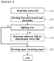
- FIG. 1 is a schematic flow chart showing a transfer and a lighting test for a light emitting diode among a method of fabricating a light emitting diode display device according to an embodiment of the present disclosure.
- a subpixel circuit including a transistor is formed on a substrate, and a light emitting diode (LED) emitting a light toward a front of the substrate is disposed on each subpixel.
- the LED has a state of epitaxial growth on a wafer including at least one of sapphire, silicon carbide (SiC), silicon (Si), gallium arsenide (GaAs), gallium nitride (GaN), zinc oxide (ZnO), silicon (Si), gallium phosphide (GaP), indium phosphide (InP), germanium (Ge) and gallium oxide (Ga2O3) and is transferred onto each subpixel of the substrate.
- SiC silicon carbide
- Si silicon
- GaAs gallium arsenide
- GaN gallium nitride
- ZnO zinc oxide
- silicon Si
- GaP gallium phosphide
- InP indium phosphide
- Ge germanium
- Ga2O3 gallium oxide
- first and second pad electrodes are formed on the LED.
- the first pad electrode contacts a first-first semiconductor layer of the LED to supply a data signal to the LED
- the second pad electrode contacts a second semiconductor layer of the LED to supply a common signal to the LED
- a lighting test for the LED is performed in a third step st3.
- the lighting test it is inspected whether the LED is deteriorated or not through various methods. For example, it may be judged in the lighting test whether the LED is deteriorated or not by verifying conduction of the LED through a probe.
- the LED may be judged in the lighting test whether the LED is deteriorated or not by verifying lighting of the LED through applying a driving signal to the first and second pad electrodes of the LED.
- the second step of forming the first and second pad electrodes may be omitted.
- a visual inspection method may be adopted or a method of detecting an area where an electric shortage occurs by flowing a current may be adopted as the lighting test according to whether the LED is deteriorated or not.
- the lighting test is not limited thereto, and any method where the deteriorated LED is detected may be adopted.
- the LED judged as a positive one "Ok" in the lighting test is transmitted to a fifth step st5.
- an insulating layer or a light converting layer for protecting the first and second pad electrodes and the LED is formed on the LED.
- the LED judged as a deteriorated one "No" in the lighting test of the third step st3 is transmitted to a repairing process of a fourth step st4.
- the repairing process is performed by disposing a sub LED on the LED judged as a deteriorated one.
- a deteriorated LED an additional process of removing the LED judged as a deteriorated one (hereinafter, a deteriorated LED) is omitted, and the first and second pad electrodes of the deteriorated LED and the sub LED are electrically connected to each other.
- the LED display device According to an embodiment of the present disclosure, deterioration of a display quality due to a deteriorated pixel is prevented. In addition, since the deteriorated LED is not required to be removed, a fabrication cost is reduced and a process efficiency is improved.
- the LED through the completed repairing process is transmitted to the fifth step st5, the transfer of the LED and the lighting test are completed by forming an insulating layer or a light converting layer for protecting the first and second pad electrodes and the LED on the LED.
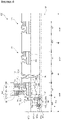
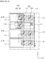
- FIG. 2 is a schematic cross-sectional view showing three subpixels of a light emitting diode display device according to a first embodiment of the present disclosure.
- a driving thin film transistor DTr and a switching thin film transistor are disposed in each subpixel R-SP, G-SP and B-SP defined on a substrate 101, the driving thin film transistor DTr is shown in one subpixel R-SP, G-SP and B-SP for convenience of illustration and conciseness of drawing.
- each of the plurality of subpixels R-SP, G-SP and B-SP may be defined by a crossing structure of data lines and gate lines, it is not limited thereto.
- each of subpixels R-SP, G-SP and B-SP includes an emitting area EA corresponding to a light emitting diode 120 and a non-emitting area NEA along a boundary of the emitting area EA.
- a switching area TrA where a driving thin film transistor DTr is formed is disposed at one side of the non-emitting area NEA.
- a semiconductor layer 103 is disposed in the switching area TrA.
- the semiconductor layer 103 includes silicon and has an active region 103a at a center thereof and source and drain regions 103b and 103c at both sides of the active region 103a.
- the active region 103a constitutes a channel and the source and drain regions 103b and 103c are doped with impurities of a high concentration.
- a gate insulating layer 105 is disposed on the semiconductor layer 103.
- a gate electrode 104 is disposed on the gate insulating layer 105 corresponding to the active region 103a of the semiconductor layer 103.
- a first interlayer insulating layer 106a is disposed on the gate electrode 104.
- the first interlayer insulating layer 106a and the gate insulating layer 105 have first and second semiconductor contact holes 107a and 107b exposing the source and drain regions 103b and 103c, respectively.
- Source and drain electrodes 109a and 109b spaced apart from each other are disposed on the first interlayer insulating layer 106a having the first and second semiconductor contact holes 107a and 107b.
- the source and drain electrodes 109a and 109b contact the source and drain regions 103b and 103c through the first and second semiconductor contact holes 107a and 197b, respectively.
- the source electrode 109a is connected to a data line, and a common line 108 parallel to the data line is disposed on the first interlayer insulating layer 106a.
- the common line 108 may be disposed in each of a plurality of unit pixels.
- at least three subpixels R-SP, G-SP and B-SP constituting each unit pixel share one common line 108.
- a number of the common lines 108 for driving each subpixel R-SP, G-SP and B-SP may be reduced.
- An aperture ratio of each unit pixel increases or a size of each unit pixel decreases according to the reduced number of the common lines 108.
- a second interlayer insulating layer 106b is disposed on the source and drain electrodes 109a and 109b, the common line 108 and the first interlayer insulating layer 106a exposed through the source and drain electrodes 109a and 109b.
- the source and drain electrodes 109a and 109b, the semiconductor layer 103 including the source and drain regions 103b and 103c contacting the source and drain electrodes 109a and 109b, the gate insulating layer 105 on the semiconductor layer 103 and the gate electrode 104 constitute the driving thin film transistor DTr.
- the switching thin film transistor has the same structure as the driving thin film transistor DTr and may be electrically connected to the driving thin film transistor DTr.
- the switching thin film transistor and the driving thin film transistor DTr exemplarily have a top gate type where the semiconductor layer 103 includes a polycrystalline silicon semiconductor layer or an oxide semiconductor layer in the drawing
- the switching thin film transistor and the driving thin film transistor DTr may have a bottom gate type where the semiconductor layer 103 includes intrinsic amorphous silicon and impurity-doped amorphous silicon in another embodiment.
- a light emitting diode (LED) 120 is disposed in each subpixel R-SP, G-SP and B-SP on the second interlayer insulating layer 106b.
- Each LED 120 includes a first n-type electrode 121, an emitting layer and a first p-type electrode 129.
- the emitting layer emits a light due to recombination of an electron and a hole according to a current flowing between the first n-type electrode 121 and the first p-type electrode 129.
- the emitting layer includes a first-first semiconductor layer 123, a first active layer 125 and a first-second semiconductor layer 127.
- the first-first semiconductor layer 123 supplies an electron to the first active layer 125.
- the first-first semiconductor layer 123 may include a semiconductor material of an n-type gallium nitride (n-GaN) group, and an n-type gallium nitride group may include gallium nitride (GaN), aluminum gallium nitride (AlGaN), indium gallium nitride (InGaN) or aluminum indium gallium nitride (AlInGaN), etc.
- the impurity used for doping the first-first semiconductor layer 123 may include silicon (Si), germanium (Ge), selenium (Se), tellurium (Te) or carbon (C), etc.
- the first active layer 125 is disposed on one side of the first-first semiconductor layer 123.
- the first active layer 125 has a multi quantum well (MQW) structure including a well layer and a barrier layer having a band gap greater than the well layer.
- MQW multi quantum well
- the first active layer 125 may have a multi quantum well structure of indium gallium nitride/gallium nitride (InGaN/GaN), etc.
- the first-second semiconductor layer 127 is disposed on the first active layer 125 and supplies a hole to the first active layer 125.
- the first-second semiconductor layer 127 may include a semiconductor material of a p-type gallium nitride (p-GaN), and a p-type gallium nitride may include gallium nitride (GaN), aluminum gallium nitride (AlGaN), indium gallium nitride (InGaN) or aluminum indium gallium nitride (AlInGaN), etc.
- the impurity used for doping the first-second semiconductor layer 127 may include magnesium (Mg), zinc (Zn) or beryllium (Be), etc.
- the first p-type electrode 129 is disposed on the first-second semiconductor layer 127 and may be used as a cathode supplying a hole to the first-second semiconductor layer 127.
- the first n-type electrode 121 is disposed on the other side of the first-first semiconductor layer 123 to be electrically separated from the first active layer 125 and the first-second semiconductor layer 127 and may be used as an anode supplying an electron to the first-first semiconductor layer 123.
- Each of the first n-type electrode 121 and the first p-type electrode 129 may include a transparent conductive material or a reflective conductive material according to a light emission direction of the LED 120.
- the transparent conductive material may be indium tin oxide (ITO) or indium zinc oxide (IZO), etc., it is not limited thereto.
- the reflective conductive material may be a material including at least one of a metallic material such as gold (Au), tungsten (W), platinum (Pt), silicon (Si), iridium (Ir), silver (Ag), copper (Cu), nickel (Ni), titanium (Ti) or chromium (Cr), etc., and an alloy thereof, it is not limited thereto.
- each of the first n-type electrode 121 and the first p-type electrode 129 may include a reflective conductive material in a bottom emission type where a light of the LED 120 is emitted toward a direction of the substrate 101, and each of the first n-type electrode 121 and the first p-type electrode 129 may include a transparent conductive material in a top emission type where a light of the LED 120 is emitted toward an opposite direction of the substrate 101.
- each of the first n-type electrode 121 and the first p-type electrode 129 includes a transparent conductive material will be exemplarily illustrated.
- the LED 120 emits a light due to recombination of an electron and a hole according to a current flowing between the first n-type electrode 121 and the first p-type electrode 129.
- a reflecting pattern 133 may be further disposed between the first-first semiconductor layer 123 and the second interlayer insulating layer 106b of the LED 120, and an insulating pattern 131 may be disposed the reflecting pattern 133 and the first-first semiconductor layer 123.
- the reflecting pattern 133 upwardly reflects a light emitted toward a direction of the substrate 101 among a light of the LED 120 to improve a light efficiency of the LED 120.
- the reflecting pattern 133 may be disposed on the substrate 101 and may include the same material and the same layer as the gate electrode 104 of the driving thin film transistor DTr, it is not limited thereto.
- the reflecting pattern 133 on the substrate 101 may include the same material as one of electrodes of the driving thin film transistor DTr.
- a third interlayer insulating layer 106c is disposed on the LED 120 in each subpixel R-SP, G-SP and B-SP.
- the third interlayer insulating layer 106c and the second interlayer insulating layer 106b have a drain contact hole PHI exposing the drain electrode 109b of the driving thin film transistor DTr and a common contact hole PH2 exposing the common line 108.
- the third interlayer insulating layer 106c has first and second electrode contact holes 114a and 114b exposing the first n-type electrode 121 and the first p-type electrode 129, respectively, of the LED 120 in each subpixel R-SP, G-SP and B-SP.
- a first connecting electrode 111 electrically connecting the drain electrode 109b of the driving thin film transistor DTr exposed through the drain contact hole PHI and the first n-type electrode 121 of the LED 120 exposed through the first electrode contact hole 114a and a second connecting electrode 112 electrically connecting the common line 108 exposed through the common contact hole PH2 and the first p-type electrode 129 exposed through the second electrode contact hole 114b are disposed on the third interlayer insulating layer 106c.
- each of the first and second connecting electrodes 111 and 112 may include a transparent conductive oxide material such as indium tin oxide (ITO), indium zinc oxide (IZO), indium tin zinc oxide (ITZO), zinc oxide (ZO) and tin oxide (TO) for transmitting a light emitted from the active layer 125 of the LED 120, it is not limited thereto.
- a transparent conductive oxide material such as indium tin oxide (ITO), indium zinc oxide (IZO), indium tin zinc oxide (ITZO), zinc oxide (ZO) and tin oxide (TO) for transmitting a light emitted from the active layer 125 of the LED 120, it is not limited thereto.
- the first n-type electrode 121 of the LED 120 is electrically connected to the drain electrode 109b of the driving thin film transistor DTr through the first connecting electrode 111, and the first p-type electrode 129 is electrically connected to the common line 108 through the second connecting line 112 so that the LED 120 in each subpixel R-SP, G-SP and B-SP can emit a light.
- a unit pixel may be defined by combination of subpixels R-SP, G-SP and B-SP, and each subpixel R-SP, G-SP and B-SP may emit a light having various colors.
- the subpixels R-SP, G-SP and B-SP may include a red subpixel, a green subpixel and a blue subpixel.
- a red colored light may be emitted from the emitting area EA of the red subpixel R-SP
- a green colored light may be emitted from the emitting area EA of the green subpixel G-SP
- a blue colored light may be emitted from the emitting area EA of the blue subpixel B-SP.
- the LEDs 120 corresponding to the emitting area EA of the subpixels R-SP, G-SP and B-SP may emit a light of different colors or same colors. For example, when the LEDs 120 of the subpixels R-SP, G-SP and B-SP emit a light of different colors, the LED 120 in the red subpixel R-SP emits a red colored light, the LED 120 in the green subpixel G-SP emits a green colored light, and the LED 120 in the blue subpixel B-SP emits a blue colored light.
- the light of the LEDs 120 may be converted into a light of different colors by an optical converter such as a light converting layer on the LEDs 120 of the subpixels R-SP, G-SP and B-SP.
- the optical converter may be disposed to correspond to each subpixel R-SP, G-SP and B-SP.
- Photo acryl, silicon oxide (SiOx) or silicon nitride (SiNx) including a light converting material such as a nano fluorescent material, an organic fluorescent material or a quantum dot, etc. may be disposed on the LED 120 in each subpixel R-SP, G-SP and B-SP through an inkjet printing method or a dotting method to form a plurality of optical converters.
- a sub LED 200 is disposed over the deteriorated LED 120.
- the sub LED 200 includes a second n-type electrode 201, an emitting layer and a second p-type electrode 209.
- the emitting layer emits a light due to recombination of an electron and a hole according to a current flowing between the second n-type electrode 201 and the second p-type electrode 209.
- the emitting layer includes a second-first semiconductor layer 203, a second active layer 205 and a second-second semiconductor layer 207.
- the second-first semiconductor layer 203 supplies an electron to the second active layer 205.
- the second-first semiconductor layer 203 may include a semiconductor material of an n-type gallium nitride (n-GaN) group, and an n-type gallium nitride group may include gallium nitride (GaN), aluminum gallium nitride (AlGaN), indium gallium nitride (InGaN) or aluminum indium gallium nitride (AlInGaN), etc.
- the impurity used for doping the second-first semiconductor layer 203 may include silicon (Si), germanium (Ge), selenium (Se), tellurium (Te) or carbon (C), etc.
- the second active layer 205 is disposed on one side of the second-first semiconductor layer 203.
- the second active layer 205 has a multi quantum well (MQW) structure including a well layer and a barrier layer having a band gap greater than the well layer.
- MQW multi quantum well
- the second active layer 205 may have a multi quantum well structure of indium gallium nitride/gallium nitride (InGaN/GaN), etc.
- the second-second semiconductor layer 207 is disposed on the second active layer 205 and supplies a hole to the second active layer 205.
- the second-second semiconductor layer 207 may include a semiconductor material of a p-type gallium nitride (p-GaN), and a p-type gallium nitride may include gallium nitride (GaN), aluminum gallium nitride (AlGaN), indium gallium nitride (InGaN) or aluminum indium gallium nitride (AlInGaN), etc.
- the impurity used for doping the second-second semiconductor layer 207 may include magnesium (Mg), zinc (Zn) or beryllium (Be), etc.
- the second p-type electrode 209 is disposed on the second-second semiconductor layer 207 and may be used as a cathode supplying a hole to the second-second semiconductor layer 207.
- the second n-type electrode 201 is disposed on the other side of the second-first semiconductor layer 203 to be electrically separated from the second active layer 205 and the second-second semiconductor layer 207 and may be used as an anode supplying an electron to the second-first semiconductor layer 203.
- the sub LED 200 is disposed over the LED 120 so that the second n-type electrode 201 can be electrically connected to the first connecting electrode 111 and the second p-type electrode 209 can be electrically connected to the second connecting electrode 112.
- a first bump 115a may be disposed between the first connecting electrode 111 and the second n-type electrode 201 and a second bump 115b may be disposed between the second connecting electrode 112 and the second p-type electrode 209.
- the sub LED 200 is disposed over the LED 120.
- the second n-type electrode 201 of the sub LED 200 is electrically connected to the first connecting electrode 111 through the first bump 115a to be electrically connected to the first n-type electrode 121 of the LED 120.
- the second p-type electrode 209 of the sub LED 200 is electrically connected to the second connecting electrode 112 through the second bump 115b to be electrically connected to the first p-type electrode 129 of the LED 120.
- a reflecting layer 211 is further disposed between the second-second semiconductor layer 207 and the second p-type electrode 209 of the sub LED 200.
- the LED display device 100 when a voltage is applied to the red subpixel R-SP, the voltage is applied to the first n-type and first p-type electrodes 121 and 129 of the LED 120 through the first and second connecting electrodes 111 and 112. However, since the LED 120 in the red subpixel R-SP is deteriorated, the LED 120 in the red subpixel R-SP does not emit a light even when the voltage is applied.
- the sub LED 200 emits a light.
- the LED display device 100 even when an additional process of removing the deteriorated LED 120 is not performed, reduction of a display quality due to the deteriorated pixel is prevented.
- the reflecting layer 211 may include a metallic material such as aluminum (Al) or silver (Ag), and it is not limited thereto.
- a second-first semiconductor layer 303 of a sub LED 300 may include a semiconductor material of a p-type gallium nitride (p-GaN) such as gallium nitride (GaN), aluminum gallium nitride (AlGaN), indium gallium nitride (InGaN) or aluminum indium gallium nitride (AlInGaN), etc.
- a second-second semiconductor layer 307 may include a semiconductor material of an n-type gallium nitride (n-GaN) group such as gallium nitride (GaN), aluminum gallium nitride (AlGaN), indium gallium nitride (InGaN) or aluminum indium gallium nitride (AlInGaN), etc.
- a second p-type electrode 309 may be disposed on the second-first semiconductor layer 303, and a second n-type electrode 301
- the sub LED 300 is disposed over a deteriorated LED 120 so that the second p-type electrode 309 of the sub LED 300 can be electrically connected to a second connecting electrode 112 connected to a first p-type electrode 129 of the LED 120 and the second n-type electrode 301 can be electrically connected to a first connecting electrode 111 connected to a first n-type electrode 121 of the LED 120.
- the reflecting layer 311 is disposed between the second n-type electrode 301 and the second-second semiconductor layer 307.
- the sub LED 200 and 300 electrically connected to the first and second connecting electrodes 111 and 112 for applying a voltage to the LED 120 is disposed over the deteriorated LED 120, deterioration of a display quality due to a deteriorated pixel is prevented without removing the deteriorated LED 120. Therefore, a fabrication cost is reduced and a process efficiency is improved.
- the LED display device 100 having a high resolution is obtained.
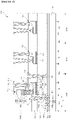
- FIG. 4 is a schematic cross-sectional view showing three subpixels of a light emitting diode display device according to a second embodiment of the present disclosure.
- a driving thin film transistor DTr including source and drain electrodes 109a and 109b, a semiconductor layer 103 having source and drain regions 103b and 103c contacting the source and drain electrodes 109a and 109b, a gate insulating layer 105 on the semiconductor layer 103 and a gate electrode 104 is disposed in a switching area TrA at one side of a non-emitting area NEA.
- a common line 108 is disposed on a first interlayer insulating layer 106a on the gate insulating layer 105 at one side of the driving thin film transistor DTr.
- a light emitting diode 120 is disposed on a second interlayer insulating layer 106b over the driving thin film transistor DTr, and a third interlayer insulating layer 106c is disposed on the LED 120.
- a first n-type electrode 121 of the LED 120 is electrically connected to the drain electrode 109b of the driving thin film transistor DTr through a first electrode contact hole 114a of the third interlayer insulating layer 106c and a drain contact hole PHI of the second and third interlayer insulating layers 106b and 106c.
- the first n-type electrode 121 and the drain electrode 109b are electrically connected to each other through a first connecting electrode 111.
- a first p-type electrode 129 of the LED 120 is electrically connected to the common line 108 through a second electrode contact hole 114b of the third interlayer insulating layer 106c and a common contact hole PH2 of the second and third interlayer insulating layers 106b and 106c.
- the first p-type electrode 129 and the common line 108 are electrically connected to each other through a second connecting electrode 112.
- the LED 120 includes a first-first semiconductor layer 123 connected to the first n-type electrode 121, a first-second semiconductor layer 127 connected to the first p-type electrode 129 and a first active layer 125 disposed between the first-first and first-second semiconductor layers 123 and 127.
- a sub LED 400 is further disposed over the deteriorated LED 120.
- a second-first semiconductor layer 403, a second active layer 405, a second-second semiconductor layer 407 and a reflecting layer 411 are disposed between a second n-type electrode 401 and a second p-type electrode 409.
- the reflecting layer 411, the second-first semiconductor layer 403, the second active layer 405, the second-second semiconductor layer 407 and the second p-type electrode 409 are sequentially disposed on the second n-type electrode 401.
- the first-first semiconductor layer 123 of the LED 120 and the second-first semiconductor layer 403 of the sub LED 400 may include a semiconductor material of an n-type gallium nitride (n-GaN) group
- the first-second semiconductor layer 127 of the LED 120 and the second-second semiconductor layer 407 of the sub LED 400 may include a semiconductor material of a p-type gallium nitride (p-GaN).
- the second n-type electrode 401 of the sub LED 400 is electrically connected to the first connecting electrode 111 connecting the first n-type electrode 121 of the LED 120 and the drain electrode 109b of the driving thin film transistor DTr.
- a bump 115 may be disposed between the second n-type electrode 401 and the first connecting electrode 111.
- a fourth interlayer insulating layer 106d is disposed on the sub LED 400, and the fourth interlayer insulating layer 106d has a third contact hole 114c exposing the second p-type electrode 409 and a fourth electrode contact hole 114d exposing the second connecting electrode 112.
- the second p-type electrode 409 exposed through the third electrode contact hole 114c and the second connecting electrode 112 exposed through the fourth electrode contact hole 114d are electrically connected to each other through a third connecting electrode 113 on the fourth interlayer insulating layer 106d.
- the LED display device 100 when a voltage is applied to the red subpixel R-SP, the voltage is applied to the first n-type and first p-type electrodes 121 and 129 of the LED 120 through the first and second connecting electrodes 111 and 112. However, since the LED 120 in the red subpixel R-SP is deteriorated, the LED 120 in the red subpixel R-SP does not emit a light even when the voltage is applied.
- the sub LED 400 emits a light.
- the LED display device 100 even when an additional process of removing the deteriorated LED 120 is not performed, reduction of a display quality due to the deteriorated pixel is prevented.
- the fourth interlayer insulating layer 106d on the sub LED 400 is formed over a whole surface of the substrate 101 in the second embodiment of the present disclosure, the fourth interlayer insulating layer 106d may be formed to correspond to the red subpixel R-SP having the sub LED 400 by patterning.
- a lighting test of the LED 120 in each subpixel R-SP, G-SP and B-SP may be performed by applying a signal to each LED 120 through a probe.
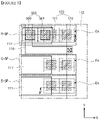
- FIGs. 5 and 6 are schematic plan views showing three subpixels of a light emitting diode display device according to a third embodiment of the present disclosure
- FIG. 7 is a schematic cross-sectional view, taken along a line V-V' of FIGs. 5 and 6 , showing three subpixels of a light emitting diode display device according to a third embodiment of the present disclosure.
- one unit pixel may be defined as three subpixels R-SP, G-SP and B-SP.
- a light emitting diode 120 is disposed in an emitting area EA in each subpixel R-SP, G-SP and B-SP.
- a first connecting electrode 111 for supplying a data signal to the LED 120 and a second connecting electrode 112 for supplying a common voltage to the LED 120 are disposed in each subpixel R-SP, G-SP and B-SP.
- the first connecting electrode 111 may be connected to the first n-type electrode 121 of an anode of the LED 120, and the second connecting electrode 112 may be connected to the first p-type electrode 129 of a cathode of the LED 120.
- the second connecting electrodes 112 of the subpixels R-SP, G-SP and B-SP are connected to each other and the LEDs 112 share one second connecting electrode 112, the second connecting electrode 112 may be disposed to be divided in each subpixels R-SP, G-SP and B-SP.
- a subLED 500 is disposed over the deteriorated LED 120.
- the first n-type electrode 121 and the first p-type electrode 129 of the LED 120 disposed in each subpixel R-SP, G-SP and B-SP are disposed along a first direction X defined in a drawing.
- the second n-type electrode 501 and the second p-type electrode 509 of the sub LED 500 over the deteriorated LED 120 among the LEDs 120 may be disposed along a first direction X defined in a drawing.
- the second n-type electrode 501 and the second p-type electrode 509 of the sub LED 500 may be disposed along a second direction Y different from the first direction X.
- the second direction Y may be perpendicular to the first direction X.
- the second n-type electrode 501 of the sub LED 500 may be electrically connected to the first connecting electrode 111, and the second p-type electrode 509 of the sub LED 500 may be electrically connected to an auxiliary electrode 116 extending from the second connecting electrode 112.
- the auxiliary electrode 116 may be formed to extend from the second connecting electrode 112, or may be formed by a jumping type through a via hole.
- the auxiliary electrode 116 may be formed by various methods.
- the auxiliary electrode 116 may be formed to have the same material and the same layer as the first and second connecting electrodes 111 and 112, or may be formed to have the same material and the same layer as one of other electrodes.
- a repair area RA may be defined between the red subpixel R-SP and the adjacent green subpixel G-SP.
- the red R-SP and the green subpixel G-SP may share the repair area RA.
- the sub LED 500 is disposed through the red subpixel R-SP and the repair RA along the second direction Y defined in a drawing.
- the sub LED 500 corresponding to the green subpixel G-SP may be disposed through the green subpixel G-SP and the repair area RA along the second direction Y defined in a drawing.
- the repair area RA may be designed in a portion adjacent to the deteriorated subpixel R-SP, G-SP and B-SP.
- a driving thin film transistor DTr including source and drain electrodes 109a and 109b, a semiconductor layer 103 having source and drain regions 103b and 103c contacting the source and drain electrodes 109a and 109b, a gate insulating layer 105 on the semiconductor layer 103 and a gate electrode 104 is disposed in a switching area TrA at one side of a non-emitting area NEA of each subpixel R-SP, G-SP and B-SP on a substrate 101.
- a common line 108 is disposed on a first interlayer insulating layer 106a on the gate insulating layer 105 at one side of the driving thin film transistor DTr.
- a light emitting diode 120 is disposed on a second interlayer insulating layer 106b over the driving thin film transistor DTr, and a third interlayer insulating layer 106c is disposed on the LED 120.
- a first n-type electrode 121 of the LED 120 is electrically connected to the drain electrode 109b of the driving thin film transistor DTr through a first electrode contact hole 114a of the third interlayer insulating layer 106c and a drain contact hole PHI of the second and third interlayer insulating layers 106b and 106c.
- the first n-type electrode 121 and the drain electrode 109b are electrically connected to each other through a first connecting electrode 111.
- a first p-type electrode 129 of the LED 120 is electrically connected to the common line 108 through a second electrode contact hole 114b of the third interlayer insulating layer 106c and a common contact hole PH2 of the second and third interlayer insulating layers 106b and 106c.
- the first p-type electrode 129 and the common line 108 are electrically connected to each other through a second connecting electrode 112.
- An auxiliary electrode 116 electrically connected to the second connecting electrode 112 is further disposed in a repair area RA defined at one side of the first connecting electrode 111 on the third interlayer insulating layer 106c.
- the LED 120 includes a first-first semiconductor layer 123 connected to the first n-type electrode 121, a first-second semiconductor layer 127 connected to the first p-type electrode 129 and a first active layer 125 disposed between the first-first and first-second semiconductor layers 123 and 127.
- a sub LED 500 is further disposed over the deteriorated LED 120.
- a second-first semiconductor layer 503, a second active layer 505, a second-second semiconductor layer 507 and a reflecting layer 211 are disposed between a second n-type electrode 501 and a second p-type electrode 509.
- the first-first semiconductor layer 123 of the LED 120 and the second-first semiconductor layer 503 of the sub LED 500 may include a semiconductor material of an n-type gallium nitride (n-GaN) group
- the first-second semiconductor layer 127 of the LED 120 and the second-second semiconductor layer 507 of the sub LED 500 may include a semiconductor material of a p-type gallium nitride (p-GaN).
- the second n-type electrode 201 of the sub LED 500 is electrically connected to the first connecting electrode 111 connecting the first n-type electrode 121 of the LED 120 and the drain electrode 109b of the driving thin film transistor DTr.
- a first bump 115a may be disposed between the second n-type electrode 501 and the first connecting electrode 111.
- the second p-type electrode 509 of the sub LED 500 is electrically connected to the auxiliary electrode 116 electrically connected to the second connecting electrode 112 connecting the first p-type electrode 129 of the LED 120 and the common line 108.
- a second bump115b may be disposed between the second p-type electrode 509 and the auxiliary electrode 116.
- the LED display device 100 when a voltage is applied to the red subpixel R-SP, the voltage is applied to the first n-type and first p-type electrodes 121 and 129 of the LED 120 through the first and second connecting electrodes 111 and 112. However, since the LED 120 in the red subpixel R-SP is deteriorated, the LED 120 in the red subpixel R-SP does not emit a light even when the voltage is applied.
- the sub LED 500 emits a light.
- the LED display device 100 even when an additional process of removing the deteriorated LED 120 is not performed, reduction of a display quality due to the deteriorated pixel is prevented.
- the sub LED 500 is formed through the LED 120 transferred in each subpixel R-SP, G-SP and B-SP on the substrate 101 having the driving thin film transistor DTr, an additional sub LED 500 is not required and a process efficiency is further improved.
Landscapes
- Devices For Indicating Variable Information By Combining Individual Elements (AREA)
- Led Devices (AREA)
Applications Claiming Priority (2)
| Application Number | Priority Date | Filing Date | Title |
|---|---|---|---|
| KR1020190176217A KR102756970B1 (ko) | 2019-12-27 | 2019-12-27 | Led 표시장치 |
| PCT/KR2020/011761 WO2021132842A1 (ko) | 2019-12-27 | 2020-09-02 | Led 표시장치 |
Publications (2)
| Publication Number | Publication Date |
|---|---|
| EP4084079A1 true EP4084079A1 (de) | 2022-11-02 |
| EP4084079A4 EP4084079A4 (de) | 2024-01-10 |
Family
ID=76575589
Family Applications (1)
| Application Number | Title | Priority Date | Filing Date |
|---|---|---|---|
| EP20907800.5A Pending EP4084079A4 (de) | 2019-12-27 | 2020-09-02 | Led-anzeigevorrichtung |
Country Status (5)
| Country | Link |
|---|---|
| US (1) | US11990458B2 (de) |
| EP (1) | EP4084079A4 (de) |
| KR (1) | KR102756970B1 (de) |
| CN (1) | CN114616673A (de) |
| WO (1) | WO2021132842A1 (de) |
Families Citing this family (6)
| Publication number | Priority date | Publication date | Assignee | Title |
|---|---|---|---|---|
| TWI720725B (zh) * | 2019-12-11 | 2021-03-01 | 財團法人工業技術研究院 | 畫素結構及其製造方法、以及具有此種畫素結構的顯示器 |
| TWI798938B (zh) * | 2021-11-16 | 2023-04-11 | 友達光電股份有限公司 | 顯示裝置 |
| CN114899298B (zh) * | 2022-07-12 | 2022-10-25 | 诺视科技(苏州)有限公司 | 一种像素单元及其制作方法、微显示屏、分立器件 |
| KR20240084305A (ko) * | 2022-12-06 | 2024-06-13 | 엘지디스플레이 주식회사 | 표시 장치 |
| US20240222386A1 (en) * | 2022-12-28 | 2024-07-04 | Silicon Display Technology | Display device and method of manufacturing the same |
| CN119208312A (zh) * | 2023-06-26 | 2024-12-27 | 联华电子股份有限公司 | 半导体结构以及其制作方法 |
Family Cites Families (10)
| Publication number | Priority date | Publication date | Assignee | Title |
|---|---|---|---|---|
| JP3747807B2 (ja) * | 2001-06-12 | 2006-02-22 | ソニー株式会社 | 素子実装基板及び不良素子の修復方法 |
| JP2006313825A (ja) | 2005-05-09 | 2006-11-16 | Sony Corp | 表示装置および表示装置の製造方法 |
| US9480133B2 (en) | 2010-01-04 | 2016-10-25 | Cooledge Lighting Inc. | Light-emitting element repair in array-based lighting devices |
| US9899329B2 (en) | 2010-11-23 | 2018-02-20 | X-Celeprint Limited | Interconnection structures and methods for transfer-printed integrated circuit elements with improved interconnection alignment tolerance |
| TWI523216B (zh) | 2011-07-13 | 2016-02-21 | 晶元光電股份有限公司 | 發光元件 |
| JP5906132B2 (ja) | 2012-05-09 | 2016-04-20 | 株式会社ジャパンディスプレイ | 表示装置 |
| US10381335B2 (en) * | 2014-10-31 | 2019-08-13 | ehux, Inc. | Hybrid display using inorganic micro light emitting diodes (uLEDs) and organic LEDs (OLEDs) |
| KR20160028436A (ko) * | 2016-02-26 | 2016-03-11 | 에피스타 코포레이션 | 발광 소자 |
| CN107507926B (zh) * | 2017-08-30 | 2020-04-03 | 深圳市华星光电半导体显示技术有限公司 | Oled像素结构及其修复方法 |
| TWI641126B (zh) * | 2017-12-04 | 2018-11-11 | Au Optronics Corp. | 畫素結構 |
-
2019
- 2019-12-27 KR KR1020190176217A patent/KR102756970B1/ko active Active
-
2020
- 2020-09-02 EP EP20907800.5A patent/EP4084079A4/de active Pending
- 2020-09-02 US US17/421,684 patent/US11990458B2/en active Active
- 2020-09-02 CN CN202080073655.5A patent/CN114616673A/zh active Pending
- 2020-09-02 WO PCT/KR2020/011761 patent/WO2021132842A1/ko not_active Ceased
Also Published As
| Publication number | Publication date |
|---|---|
| WO2021132842A1 (ko) | 2021-07-01 |
| KR20210083680A (ko) | 2021-07-07 |
| CN114616673A (zh) | 2022-06-10 |
| US11990458B2 (en) | 2024-05-21 |
| US20220320055A1 (en) | 2022-10-06 |
| EP4084079A4 (de) | 2024-01-10 |
| KR102756970B1 (ko) | 2025-01-17 |
Similar Documents
| Publication | Publication Date | Title |
|---|---|---|
| US11990458B2 (en) | Light emitting diode display device | |
| US11842681B2 (en) | Display device and method of manufacturing the same | |
| US11094867B2 (en) | Display device and method of manufacturing the same | |
| US11227984B2 (en) | Display device having a plurality of main pads, a plurality of redundant pads, and a light-emitting device in a display area | |
| CN109904303B (zh) | 发光器件以及使用该发光器件的显示装置 | |
| US12218300B2 (en) | Light emitting diode display device and method of fabricating light emitting diode display device | |
| KR102784887B1 (ko) | 표시장치 | |
| US12324294B2 (en) | Light emitting diode display device | |
| KR20210083681A (ko) | Led 표시장치 | |
| GB2611858A (en) | Display device | |
| US20230215975A1 (en) | Nanorod light emitting element and display device including the same | |
| US20230061844A1 (en) | Pad structure, display device, and manufacturing method thereof | |
| US20240282804A1 (en) | Display module and manufacturing method therefor | |
| US20250031504A1 (en) | Method of manufacturing display device and display device | |
| KR102788148B1 (ko) | Led 표시장치 및 이의 제조방법 | |
| US20240372053A1 (en) | Light-emitting device and display device having the same | |
| KR102878396B1 (ko) | 표시 장치 | |
| EP4160701A1 (de) | Mikro-led und anzeigemodul damit | |
| KR20260031923A (ko) | Led 표시장치 및 이의 제조방법 | |
| KR20250125560A (ko) | 마이크로 led 표시패널 및 표시장치 | |
| KR20250131561A (ko) | 마이크로 led 표시장치 및 이의 검사 방법 | |
| CN118412364A (zh) | 显示装置及制造该显示装置的方法 |
Legal Events
| Date | Code | Title | Description |
|---|---|---|---|
| STAA | Information on the status of an ep patent application or granted ep patent |
Free format text: STATUS: THE INTERNATIONAL PUBLICATION HAS BEEN MADE |
|
| PUAI | Public reference made under article 153(3) epc to a published international application that has entered the european phase |
Free format text: ORIGINAL CODE: 0009012 |
|
| STAA | Information on the status of an ep patent application or granted ep patent |
Free format text: STATUS: REQUEST FOR EXAMINATION WAS MADE |
|
| 17P | Request for examination filed |
Effective date: 20220428 |
|
| AK | Designated contracting states |
Kind code of ref document: A1 Designated state(s): AL AT BE BG CH CY CZ DE DK EE ES FI FR GB GR HR HU IE IS IT LI LT LU LV MC MK MT NL NO PL PT RO RS SE SI SK SM TR |
|
| DAV | Request for validation of the european patent (deleted) | ||
| DAX | Request for extension of the european patent (deleted) | ||
| A4 | Supplementary search report drawn up and despatched |
Effective date: 20231212 |
|
| RIC1 | Information provided on ipc code assigned before grant |
Ipc: H01L 33/46 20100101ALI20231206BHEP Ipc: H01L 25/075 20060101ALI20231206BHEP Ipc: H01L 33/60 20100101ALI20231206BHEP Ipc: H01L 21/768 20060101ALI20231206BHEP Ipc: H01L 25/16 20060101ALI20231206BHEP Ipc: H01L 27/15 20060101AFI20231206BHEP |