EP4084403A1 - Schaltelement und schaltvorrichtung - Google Patents
Schaltelement und schaltvorrichtung Download PDFInfo
- Publication number
- EP4084403A1 EP4084403A1 EP20914867.5A EP20914867A EP4084403A1 EP 4084403 A1 EP4084403 A1 EP 4084403A1 EP 20914867 A EP20914867 A EP 20914867A EP 4084403 A1 EP4084403 A1 EP 4084403A1
- Authority
- EP
- European Patent Office
- Prior art keywords
- data stream
- switch fabric
- data
- mac layer
- switch
- Prior art date
- Legal status (The legal status is an assumption and is not a legal conclusion. Google has not performed a legal analysis and makes no representation as to the accuracy of the status listed.)
- Granted
Links
Images


Classifications
-
- H—ELECTRICITY
- H04—ELECTRIC COMMUNICATION TECHNIQUE
- H04L—TRANSMISSION OF DIGITAL INFORMATION, e.g. TELEGRAPHIC COMMUNICATION
- H04L49/00—Packet switching elements
- H04L49/25—Routing or path finding in a switch fabric
-
- H—ELECTRICITY
- H04—ELECTRIC COMMUNICATION TECHNIQUE
- H04L—TRANSMISSION OF DIGITAL INFORMATION, e.g. TELEGRAPHIC COMMUNICATION
- H04L49/00—Packet switching elements
- H04L49/15—Interconnection of switching modules
Definitions
- This application relates to the field of switch fabric technologies, and in particular, to a switch fabric chip and a switch device.
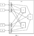
- a switch fabric interface chip (fabric interface card, FIC) needs to be fully connected to all switch units (switch element, SE). As shown in FIG. 1 , that is, for each FIC, the FIC needs to be connected to all SEs in a switch fabric unit (switch fabric unit, SFU).
- the SE may also be referred to as a switch fabric chip or a network chip, and the FIC may also be referred to as a line plug chip or a line card.
- a data switch solution is urgently needed, so as to reduce costs and power consumption of a switch device on a premise of improving accuracy of data transmission between a FIC and a remote SE.
- Embodiments of this application provide a switch fabric chip and a switch device, so as to reduce costs and power consumption of the switch device on a premise of improving accuracy of data transmission between a FIC and a remote SE.
- an embodiment of this application provides a switch fabric chip, including: a first medium access control MAC layer circuit, configured to: perform parsing processing on an input first data stream to obtain a second data stream, and output the second data stream to a processor and a first data selector; the processor, coupled to the first MAC layer circuit, and configured to: perform scheduling and switch processing on the second data stream to obtain a third data stream, and output the third data stream to the first data selector; the first data selector, coupled to the first MAC layer circuit and the processor, and configured to: when the first data stream is a data stream that is switched to another switch fabric chip in a switch device in which the switch fabric chip is located, select to output the second data stream, and when the first data stream is a data stream that is switched to another switch device, select to output the third data stream; and a second MAC layer circuit, coupled to the first data selector, and configured to: perform sending processing on a fourth data stream output by the first data selector, to obtain a fifth data stream.
- the switch fabric chip there are two transmission paths in the switch fabric chip.
- One transmission path is used for transmitting a data stream to another SE.
- the switch fabric chip serves as a relay SE.
- the other transmission path is used for transmitting the data stream to another switch device.
- the transmission path may be used for implementing an existing function of the SE, that is, implementing data switch between switch devices. That is, the switch fabric chip in the first aspect may be configured to implement a function of an existing SE, and may also serve as a relay SE in the switch device to implement a connection between an FIC and a remote SE.
- the switch fabric chip may transmit a data stream through a specific transmission path. In this way, a processing delay of the data stream is reduced.
- the switch fabric chip provided in the first aspect, a problem of a high bit error rate caused by path loss when the FIC directly transmits a data stream to the remote SE can be avoided.
- no additional CDR chip is required to serve as a relay when this solution is used, costs and power consumption of the switch device are reduced.
- the first MAC layer circuit is further configured to: receive a first frequency deviation match cell, where the first frequency deviation match cell is used for indicating a frequency deviation between an upper-level chip of the switch fabric chip and the switch fabric chip; and perform frequency regulation on the second data stream based on the first frequency deviation match cell.
- the second MAC layer circuit is further configured to: insert, into the fifth data stream, a second frequency deviation match cell delivered by a controller in the switch device in which the switch fabric chip is located, where the second frequency deviation match cell is used for indicating a frequency deviation between the switch fabric chip and a lower-level chip of the switch fabric chip.
- the first MAC layer circuit may perform frequency regulation on the second data stream based on the first frequency deviation match cell, so that the second data stream is applicable to an operating frequency of the switch fabric chip.
- the second MAC layer circuit may also insert the second frequency deviation match cell into the fifth data stream, so that the lower-level chip may perform frequency regulation on the received data stream based on the second frequency deviation match cell.
- the first MAC layer circuit may first perform frequency regulation on the first data stream based on the first frequency deviation match cell, and then perform parsing processing on the first data stream on which frequency regulation is performed, to obtain the second data stream.
- a sequence of performing frequency regulation and parsing processing by the first MAC layer circuit is not limited.
- a sequence of performing frequency regulation and sending processing by the second MAC layer circuit is also not limited.
- the switch fabric chip provided in the first aspect may further include: a first PCS circuit, configured to: receive a sixth data stream from at least one first chip interface of the switch fabric chip, perform forward error correction FEC coding and cell delineation to obtain the first data stream, and output the first data stream to the first MAC layer circuit; and a second PCS circuit, coupled to the second MAC layer circuit, and configured to: perform encoding processing on the fifth data stream to obtain a seventh data stream, and output the seventh data stream to at least one second chip interface of the switch fabric chip.
- a first PCS circuit configured to: receive a sixth data stream from at least one first chip interface of the switch fabric chip, perform forward error correction FEC coding and cell delineation to obtain the first data stream, and output the first data stream to the first MAC layer circuit
- a second PCS circuit coupled to the second MAC layer circuit, and configured to: perform encoding processing on the fifth data stream to obtain a seventh data stream, and output the seventh data stream to at least one second chip interface of the switch fabric chip
- the first PCS circuit is further configured to: switch a transmission sequence of at least one sub-data stream included in the sixth data stream.
- the first PCS circuit switches the transmission sequence of the sub-data stream. This can reduce difficulty of cabling inside the switch fabric chip, or reduce difficulty of cabling between the switch fabric chip and another switch fabric chip or another switch device. In this way, flexibility of data stream processing can be improved.
- the second PCS circuit is further configured to: switch a transmission sequence of at least one sub-data stream included in the seventh data stream.
- the second PCS circuit switches the transmission sequence of the sub-data stream. This can reduce difficulty of cabling inside the switch fabric chip, or reduce difficulty of cabling between the switch fabric chip and another switch fabric chip or another switch device. In this way, flexibility of data stream processing can be improved.
- the switch fabric chip provided in the first aspect may further include a selector matrix.
- the selector matrix includes NxN second data selectors arranged in an array. Every two adjacent second data selectors in the NxN second data selectors are coupled.
- the selector matrix is coupled to N first MAC layer circuits and N second MAC layer circuits that are included in the switch fabric chip, and is configured to output, to any one of the N second MAC layer circuits, a data stream input by any one of the N first MAC layer circuits, and N ⁇ 1.
- the first MAC layer circuit When performing parsing processing on an input data stream and outputting a parsed data stream to the first data selector, the first MAC layer circuit is specifically configured to: the first MAC layer circuit performs parsing processing on the input data stream, and outputs the parsed data stream to the first data selector by using the selector matrix.
- That the selector matrix is coupled to the N first MAC layer circuits and the N second MAC layer circuits may mean that some of the NxN second data selectors are separately connected to the N first MAC layer circuits, and some of the NxN second data selectors are separately connected to the N second MAC layer circuits.
- some second data selectors are connected to only the first MAC layer circuit
- some second data selectors are connected to only the second MAC layer circuit
- some second data selectors are connected to both the first MAC layer circuit and the second MAC layer circuit
- some second data selectors are not connected to either the first MAC layer circuit or the second MAC layer circuit.
- the switch fabric chip when the switch fabric chip includes a relatively large quantity of MAC layer circuits, data stream transmission between any two MAC layer circuits 404 may be implemented by using one selector matrix. In this way, complexity of signal cabling is reduced, and flexibility of data stream transmission is improved.
- Each of the NxN second data selectors may be a two-input two-output bidirectional data selector.
- the first MAC layer circuit and the second MAC layer circuit are chips that can perform bidirectional processing on a data stream.
- an embodiment of this application provides a switch device.
- the switch device includes a plurality of FICs and a switch fabric unit.
- the switch fabric unit is integrated with a plurality of switch fabric chips and a controller. At least one of the plurality of switch fabric chips is the switch fabric chip provided in any one of the first aspect and the possible designs of the first aspect.
- the plurality of FICs are separately directly connected to each of the plurality of switch fabric chips or are connected by using the switch fabric chip provided in any one of the first aspect and the possible designs of the first aspect.
- the controller is configured to send a control signal to a first data selector in the switch fabric chip.
- the control signal is used for indicating the first data selector to select to output a data stream input by a first MAC layer circuit or output a data stream input by a processor.
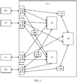
- Embodiments of this application may be applied to a switch device shown in FIG. 3 .
- the switch device includes a plurality of FICs and an SFU.
- the SFU is integrated with a plurality of SEs (that is, switch fabric chips) and one controller.
- the SE when full connection between the FIC and the SE is implemented, for an FIC and an SE that are close to each other, the SE is directly connected to the FIC (as shown by a solid line in FIG. 3 ).
- another SE may serve as a relay to implement connection between the FIC and the remote SE (as shown by a dashed line in FIG. 3 ). Therefore, for an SE that serves as a relay, a data stream output by the SE may be output to another switch device as an output of the SFU (that is, an output of the entire switch device). The data stream output by the SE may also be output to another SE on the SFU.
- the SFU is further integrated with the controller.
- the controller may control the SE. Specifically, in this embodiment of this application, the controller may control a data selector in an SE based on a target flow direction (for example, outputting to another switch device or outputting to another SE on the SFU) of a data stream transmitted in the SE, to select and output a corresponding data stream.
- a target flow direction for example, outputting to another switch device or outputting to another SE on the SFU
- the quantity of FICs in the switch device may be inconsistent with the quantity of chip interfaces in the SE.
- the quantity of chip interfaces in the SE may be far greater than the quantity of FICs. Therefore, when receiving a data stream of an FIC, the SE may simultaneously receive at least one sub-data stream from the same FIC through a plurality of chip interfaces (in this case, the FIC is separately connected to different chip interfaces in the SE through at least one physical cable). For example, eight chip interfaces in the SE separately receive eight sub-data streams from a same FIC. In this way, transmission bandwidth between the SE and the FIC is increased.
- parallel/serial conversion may be performed on at least one sub-data stream from a same FIC to form a data stream for subsequent processing.
- sequences of the sub-data streams may be exchanged.
- the SE is connected to the FIC through a physical interface on the SFU.
- the physical interface is merely an example. In actual application, the physical interface may correspond to a plurality of chip interfaces on the SFU.
- Embodiments of this application provide a switch fabric chip and a switch device, so as to reduce costs and power consumption of the switch device on a premise of improving accuracy of data transmission between a FIC and a remote SE.
- FIG. 4 is a schematic diagram of a structure of a switch fabric chip according to an embodiment of this application.
- a switch fabric chip 400 includes a first medium access control (media access control, MAC) layer circuit 401, a processor 402, a first data selector 403, and a second MAC layer circuit 404.
- MAC medium access control
- the first MAC layer circuit 401 is configured to perform parsing processing (for example, verifying a first data stream and extracting header information from the first data stream) on the input first data stream to obtain a second data stream, and output the second data stream to the processor 402 and the first data selector 403.
- the processor 402 is coupled to the first MAC layer circuit 401, and is configured to perform scheduling and switch processing on the second data stream to obtain a third data stream, and output the third data stream to the first data selector 403.
- the first data selector 403 is coupled to the first MAC layer circuit 401 and the processor 402, and is configured to: when the first data stream is a data stream that is switched to another switch fabric chip in a switch device in which the switch fabric chip 400 is located, select to output the second data stream, and when the first data stream is a data stream that is switched to another switch device, select to output the third data stream.
- the second MAC layer circuit 404 is coupled to the first data selector 403, and is configured to perform sending processing on a fourth data stream output by the first data selector 403, to obtain a fifth data stream.
- the first MAC layer circuit 401 and the second MAC layer circuit 404 may be implemented by using a logic circuit or an analog circuit.
- the first MAC layer circuit 401 may be considered as a MAC layer circuit of an ingress port, and is configured to process a data stream input to the switch fabric chip 400
- the second MAC layer circuit 404 may be considered as a MAC layer circuit of an egress port, and is configured to process the data stream to be output by the switch fabric chip 400.
- the switch fabric chip 400 there are two transmission paths for the data stream.
- One transmission path is the first MAC layer circuit 401 ⁇ the processor 402 ⁇ the first data selector 403 ⁇ the second MAC layer circuit 404.
- the other transmission path is the first MAC layer circuit 401 ⁇ the first data selector 403 ⁇ the second MAC layer circuit 404.
- the second transmission path can be output without scheduling and switch processing performed by the processor 402.
- the switch fabric chip 400 serves as a relay SE to transmit a data stream to another SE in an SFU
- the second transmission path (the first MAC layer circuit 401 ⁇ the first data selector 403 ⁇ the second MAC layer circuit 404) may be selected for transmission, and scheduling processing may not be performed on the data stream. In this way, a processing delay of the data stream is reduced.
- the switch fabric chip 400 transmits a data stream to another switch device other than the switch device in which the switch fabric chip 400 is located, the first transmission path (the first MAC layer circuit 401 ⁇ the processor 402 ⁇ the first data selector 403 ⁇ the second MAC layer circuit 404) may be selected for transmission, to implement scheduling and switch of the data stream, and then the data stream obtained through scheduling and switch is output to the another switch device.
- the first transmission path (the first MAC layer circuit 401 ⁇ the processor 402 ⁇ the first data selector 403 ⁇ the second MAC layer circuit 404) may be selected for transmission, to implement scheduling and switch of the data stream, and then the data stream obtained through scheduling and switch is output to the another switch device.
- the switch fabric chip 400 there are two transmission paths in the switch fabric chip 400.
- One transmission path is used for transmitting a data stream to another SE.
- the switch fabric chip 400 serves as a relay SE.
- the other transmission path is used for transmitting the data stream to another switch device.
- the transmission path may be used for implementing an existing function of the SE, that is, implementing data switch between switch devices.
- the switch fabric chip 400 may transmit a data stream through a specific transmission path. In this way, a processing delay of the data stream is reduced. In this manner, a problem of a high bit error rate caused by path loss when an FIC directly transmits a data stream to a remote SE can be avoided.
- no additional CDR chip is required to serve as a relay when this solution is used, costs and power consumption of the switch device are reduced.
- the switch fabric chip 400 may further include: a first physical coding sublayer (physical coding sublayer, PCS) circuit, configured to: receive a sixth data stream from at least one first chip interface of the switch fabric chip 400, perform forward error correction (forward error correction, FEC) coding and cell delineation to obtain the first data stream, and output the first data stream to the first MAC layer circuit 401; and a second PCS circuit, coupled to the second MAC layer circuit 404, and configured to: perform encoding processing on the fifth data stream to obtain a seventh data stream, and output the seventh data stream to at least one second chip interface of the switch fabric chip 400.
- a structure of the switch fabric chip 400 may be shown in FIG. 5 .
- FIG. 5 only one first chip interface and one second chip interface are used as an example for description. In actual application, there may be a plurality of first chip interfaces and a plurality of second chip interfaces.
- the first chip interface and the second chip interface are interfaces through which the switch fabric chip 400 inputs and outputs a data stream to the outside.
- the first chip interface may be an interface configured to receive a data stream
- the second chip interface may be an interface configured to output a data stream.
- the first chip interface and the second chip interface may alternatively be bidirectional transmission interfaces. That is, the first chip interface is configured to both receive and output a data stream, and the second chip interface is configured to both receive and output a data stream. If both the first chip interface and the second chip interface are bidirectional transmission interfaces, correspondingly, the first MAC layer circuit 401, the second MAC layer circuit 404, the first PCS circuit, and the second PCS circuit are also chips that can perform bidirectional processing.
- the sixth data stream received by the first PCS circuit from the at least one first chip interface may be a sixth data stream obtained after serial processing is performed on a data stream received by the at least one first chip interface by using a serializer/deserializer (serializer/deserializer, SERDES).
- the seventh data stream output by the second PCS circuit may be output to the at least one second chip interface after deserialization processing is performed by the SERDES.
- the at least one first chip interface may receive the sixth data stream from a same FIC in the switch device. That is, to increase transmission bandwidth between the FIC and the switch fabric chip 400, the FIC may transmit at least one sub-data stream in parallel. The at least one sub-data stream is separately received by the at least one first chip interface. After serial processing is performed by the SERDES, the sixth data stream is formed. Subsequent processing is performed by a circuit such as the first PCS circuit and the first MAC layer circuit in the switch fabric chip 400. Similarly, the seventh data stream on which the second PCS circuit performs encoding processing may also be deserialized by the SERDES to form at least one sub-data stream. The at least one sub-data stream is output through the at least one second chip interface, so that a lower-level chip or device performs processing.
- the first PCS circuit is further configured to: switch a transmission sequence of the at least one sub-data stream included in the sixth data stream.
- the second PCS circuit may be further configured to: switch a transmission sequence of the at least one sub-data stream included in the seventh data stream.
- a processing procedure in which the first PCS circuit switches the transmission sequence is used as an example. It is assumed that eight first chip interfaces (a first chip interface 1 to a first chip interface 8) of the switch fabric chip 400 separately receive eight sub-data streams from a same FIC, which are respectively A, B, C, D, E, F, G, and H. The eight sub-data streams form the foregoing sixth data stream. After serial processing is performed, the eight sub-data streams are transmitted to the first PCS circuit based on a transmission sequence of A, B, C, D, E, F, G and H. The first PCS circuit may adjust the sequence of the eight sub-data streams, for example, adjust the sequence to A, C, B, D, E, G, F and H. For a manner in which the second PCS circuit switches the transmission sequence of the sub-data stream, refer to the processing procedure in which the first PCS circuit switches the transmission sequence. Details are not described herein again.
- the first PCS circuit and the second PCS circuit may switch transmission sequences of the sub-data streams by using a data selector (MUX).
- MUX data selector
- the first PCS circuit and the second PCS circuit switch the transmission sequence of the sub-data stream. This can reduce difficulty of cabling inside the switch fabric chip 400 can be reduced, or difficulty of cabling between the switch fabric chip 400 and another switch fabric chip or another switch device can be reduced. In this way, flexibility of data stream processing can be improved.
- a sequence of the sub-data streams received by the first PCS circuit from the at least one first chip interface is not a sequence that complies with a real time sequence rule of the at least one first chip interface. Therefore, after receiving the sixth data stream, the first PCS circuit may adjust a transmission sequence of the at least one sub-data stream in the sixth data stream, so that the adjusted transmission sequence complies with the real time sequence rule.
- the sub-data streams should be transmitted in a sequence of A, B, C, and D. That is, A+B+C+D may be spliced into a data stream transmitted by the FIC to the switch fabric chip 400.
- A+B+C+D may be spliced into a data stream transmitted by the FIC to the switch fabric chip 400.
- the sub-data streams may be transmitted in the sequence of A, C, B, and D.
- the first PCS circuit adjusts the sequence of the sub-data streams to A, B, C, and D.
- the first MAC layer circuit 401 may be further configured to: receive a first frequency deviation match cell (frequency modulation cell, FM cell), where the first frequency deviation match cell is used for indicating a frequency deviation between an upper-level chip of the switch fabric chip and the switch fabric chip; and perform frequency regulation on the second data stream based on the first frequency deviation match cell.
- the second MAC layer circuit 404 may be further configured to: insert, into the fifth data stream, a second frequency deviation match cell delivered by a controller in the switch device in which the switch fabric chip is located, where the second frequency deviation match cell is used for indicating a frequency deviation between the switch fabric chip and a lower-level chip of the switch fabric chip.
- operating frequencies of the chips may be different.
- frequency regulation may be performed on the second data stream based on the first frequency deviation match cell, so that the second data stream is applicable to an operating frequency of the switch fabric chip 400.
- the switch fabric chip 400 may also insert the second frequency deviation match cell into the fifth data stream on which the sending processing is performed, so that the lower-level chip may perform frequency regulation on the received data stream based on the second frequency deviation match cell.
- the switch fabric chip 400 there are two transmission paths for the data stream in the switch fabric chip 400.
- One transmission path is the first MAC layer circuit 401 ⁇ the processor 402 ⁇ the first data selector 403 ⁇ the second MAC layer circuit 404.
- the other transmission path is the first MAC layer circuit 401 ⁇ the first data selector 403 ⁇ the second MAC layer circuit 404.
- the second transmission path can be output without being scheduled by the processor 402, and may be selected and used when the switch fabric chip 400 serves as the relay SE.
- the second transmission path may be implemented through a physical cable between the first MAC layer circuit 401 and the first data selector 403.
- the switch fabric chip 400 includes only the first MAC layer circuit 401 and the second MAC layer circuit 404
- the second transmission path may be implemented through a physical cable between the first MAC layer circuit 401 and the first data selector 403.
- the foregoing second transmission path may be implemented by using a selector matrix.
- the selector matrix may include NxN second data selectors arranged in an array. Every two adjacent second data selectors in the NxN second data selectors are coupled.
- the selector matrix is coupled to the N first MAC layer circuits 401 and the N second MAC layer circuits 404, and is configured to output, to any one of the N second MAC layer circuits 404, a data stream input by any one of the N first MAC layer circuits 401, and N ⁇ 1.
- Each second data selector is a two-input two-output bidirectional data selection.
- each second data selector may select an input data stream (either one), or may select an output flow direction of the data stream (either one).
- the selector matrix is coupled to the N first MAC layer circuits 401 and the N second MAC layer circuits 404, a data stream input by any first MAC layer circuit 401 may be output to any second MAC layer circuit 404 by selecting a plurality of second data selectors within the selector matrix, so as to avoid a problem of a complex physical cable that is generated when the first MAC layer circuit 401 is directly connected to the second MAC layer circuit 404 through the physical cable, and reduce an area of the switch fabric chip 400.
- the first MAC layer circuit 401 when performing parsing processing on an input data stream and outputting a parsed data stream to the first data selector 403, the first MAC layer circuit 401 is specifically configured to: the first MAC layer circuit 401 performs parsing processing on the input data stream, and outputs the parsed data stream to the first data selector 403 by using the selector matrix.
- the selector matrix may be shown in FIG. 6 .
- N ports that is, A 1 , A 2 , A 3 , ..., A N
- N ports that is, B 1 , B 2 , B 3 , ..., B N
- N second MAC layer circuits 404 N ports
- each black dot represents one second data selector.
- the second data selector may be a two-input two-output bidirectional data selector (that is, a 2x2 bidirectional data selector), as shown in FIG. 6 .
- the N ports (that is, A 1 , A 2 , A 3 , ..., A N ) on the left side may also be separately connected to the N second MAC layer circuits 404, and the N ports (that is, B 1 , B 2 , B 3 , ..., B N ) on the bottom may also be separately connected to the N first MAC layer circuits 401.
- the N ports on the left side are separately connected to the N first MAC layer circuits 401 and the N ports on the bottom are separately connected to the N second MAC layer circuits 404 is used for illustration.
- a second data selector in a second row and a second column in the selector matrix shown in FIG. 6 (that is, the second data selector drawn by using an elliptic dashed circle in FIG. 6 ) is used as an example.
- the second data selector is referred to as an N0
- a second data selector connected to the NO and located above the NO is referred to as an N1
- a second data selector connected to the NO and located on a left side of the NO is referred to as an N2
- a second data selector connected to the NO and located on a right side of the NO is referred to as an N3
- a second data selector connected to the NO and located below the NO is referred to as an N4, as shown in FIG. 6 .
- the NO may be configured to select either of data streams from the N1 and the N2, and output the selected data stream to the N3 or the N4, for example, select to output a data stream from the N1 to the N4. Because the NO is a bidirectional data selector, the NO may also be configured to select data streams from the N3 and the N4, and output the selected data stream to the N1 or the N2, for example, select to output a data stream from the N2 to the N3.
- the NO may perform the foregoing selection based on an input 2-bit configuration parameter.
- the configuration parameter may be delivered by a controller integrated on an SFU of a switch device in which a switch fabric chip 400 is located.
- a data stream input from any port of A 1 , A 2 , A 3 , ..., A N on the left side may be switched to any port of B 1 , B 2 , B 3 , ..., B N on the bottom, and a data stream input from any port of B 1 , B 2 , B 3 , ..., B N on the bottom may also be switched to any port of A 1 , A 2 , A 3 , ..., A N on the left side.
- a data stream input by any one of the N first MAC layer circuits 401 may be output to any one of the N second MAC layer circuits 404 by using the selector matrix shown in FIG. 6 .
- a data stream output by the first MAC layer circuit 401 may be input to a first data selector 403 by using the selector matrix. Further, the data stream output by the first MAC layer circuit 401 is input to the second MAC layer circuit 404 through selection of the first data selector 403.
- the switch fabric chip 400 includes the N first MAC layer circuits 401 and the N second MAC layer circuits 404
- data stream transmission between any first MAC layer circuit 401 and any second MAC layer circuit 404 may be implemented by using one selector matrix. In this way, complexity of signal cabling is reduced, and flexibility of data stream transmission is improved.
- FIG. 7 is a schematic diagram of a structure of another switch fabric chip according to an embodiment of this application.
- the switch fabric chip may be considered as a specific example of the switch fabric chip 400.
- a PCS 0, a PCS 1, and a PCS 2 may be considered as a specific example of the first PCS circuit, or may be considered as a specific example of the second PCS circuit (that is, the PCS circuit is a bidirectional PCS circuit).
- the PCS may be configured to perform data encoding and decoding processing, and may further implement switch between local links by using a data selector (MUX) in the PCS, that is, adjust a transmission sequence of at least one sub-data stream included in an input data stream.
- MUX data selector
- An MAC NO and an MAC N1 may be considered as a specific example of the first MAC layer circuit 401, or may be considered as a specific example of the second MAC layer circuit 404 (that is, the MAC layer circuit is a bidirectional MAC layer circuit).
- An MAC 0 module is mainly configured to perform parsing processing on a data stream.
- a user datagram protocol (user datagram protocol, UDP) module is mainly configured to perform protocol processing, and the MUX configured to connect the PCS and the MAC may be configured to perform bit width splicing and conversion.
- a TXDP is configured to perform parallel-to-serial processing of a data stream, and an RXDP is configured to perform serial-to-parallel processing of a data stream.
- a switch buffer (switch buffer, SWB) may be considered as a specific example of the processor 402, and is configured to perform buffer scheduling and switch of a data stream.
- a top-layer N-N switch network (represented by four black dots in FIG.
- the top-layer N-N switch network includes four second data selectors.
- the MUXs in the MAC NO and the MAC N1 may be considered as a specific example of the first data selector.
- the MUXs may be disposed inside the MAC NO and the MAC N1, or may exist independently of the MAC NO and the MAC N1. In FIG. 7 , only an example in which the MUXs are disposed inside the MAC NO and the MAC N1 is used for illustration.
- both the PCS and the MAC can perform bidirectional processing on a data stream.
- a path 1 shown by a dashed line in FIG. 7 is used as an example.
- Data streams received by a PCS 0 on the left are decoded and output to a MUX.
- some data streams are sent to the SWB for buffer scheduling, switch processing, and subsequent processing (a processing procedure of a data stream in the conventional technology).
- the other data streams are sent to the top N-N switch network, and is output to an MUX in the MAC NO after being selected by each second data selector in the top N-N switch network.
- the data stream is parsed by an MAC NO on the right, encoded by a PCS 0 on the right, and then output.
- a data stream that is not processed by the SWB may be a data stream used for switching to another switch fabric chip.
- the switch fabric chip shown in FIG. 7 is used as a relay between an FIC and the another switch fabric chip, so as to implement a connection between the switch fabric chip and the FIC.
- FIG. 7 further shows an example in which a PCS 2 on the right inputs a data stream and a PCS 2 on the left outputs the data stream when a switch fabric chip is used as a relay, that is, a path 2 shown by a dashed line in FIG. 7 .
- Atop-layer N-N switch network that the path 2 passes through and the top-layer N-N switch network that the dashed path 1 passes through may be a same switch network.
- switch between the local links may be performed by using the MUX in the PCS circuit (that is, the transmission sequence of the at least one sub-data stream included in the input data stream is adjusted), to improve flexibility of data stream processing; and top-layer switch of data streams may be further implemented by using the MUX in the selector matrix, so that the data stream to be transmitted to another switch fabric chip does not need to undergo scheduling and switch processing by the switch fabric chip 400, to reduce a delay of data stream transmission. That is, there are two levels of MUX selection inside the switch fabric chip 400. As shown in FIG. 8 , before entering a selector matrix, switch between local links is performed by using an MUX in a PCS circuit, and after entering the selector matrix, an MUX in the selector matrix selects an output path.
- the switch fabric chip 400 there are two transmission paths in the switch fabric chip 400.
- One transmission path is used for transmitting a data stream to another SE.
- the switch fabric chip 400 serves as a relay SE.
- the other transmission path is used for transmitting the data stream to another switch device.
- the transmission path may be used for implementing an existing function of the SE, that is, implementing data switch between switch devices.
- the switch fabric chip 400 provided in this embodiment of this application may be configured to implement a function of an existing SE, and may also serve as a relay SE in the switch device to implement a connection between an FIC and a remote SE.
- the switch fabric chip 400 may transmit a data stream through a specific transmission path.
- the switch fabric chip 400 provided in this embodiment of this application, a problem of a high bit error rate caused by path loss when the FIC directly transmits a data stream to the remote SE can be avoided.
- no additional CDR chip is required to serve as a relay when this solution is used, costs and power consumption of the switch device are reduced.
- switch device 900 includes a plurality of switch fabric interface chips 901 and a switch fabric unit 902.
- the switch fabric unit 902 is integrated with a plurality of switch fabric chips and a controller 902a.
- At least one of the plurality of switch fabric chips is the foregoing switch fabric chip 400.
- the plurality of switch fabric interface chips 901 are separately directly connected to each of the plurality of switch fabric chips or indirectly connected to the switch fabric chip 400.
- the controller 902a is configured to send a control signal to a first data selector in the switch fabric chip 400.
- the control signal is used for indicating the first data selector to select to output a data stream input by a first MAC layer circuit or output a data stream input by a processor.
- the switch fabric chip may all adopt the structure of the switch fabric chip 400 in FIG. 4 (this manner is shown in FIG. 9 ), or may partly adopt the structure of the switch fabric chip 400 and partly adopt a structure of a switch fabric chip in the conventional technology.
- the switch fabric interface chip 901 needs to be connected to each switch fabric chip.
- a connection manner between the switch fabric interface chip 901 and the switch fabric chip may be directly connected, or may be indirectly connected by using the switch fabric chip 400.
- the switch fabric chip 400 serves as a relay SE.
- switch device 900 for a specific processing procedure of the switch fabric chip 400, reference may be made to the description in the foregoing embodiment. Details are not described herein again.
Landscapes
- Engineering & Computer Science (AREA)
- Computer Networks & Wireless Communication (AREA)
- Signal Processing (AREA)
- Small-Scale Networks (AREA)
- Data Exchanges In Wide-Area Networks (AREA)
Applications Claiming Priority (1)
| Application Number | Priority Date | Filing Date | Title |
|---|---|---|---|
| PCT/CN2020/073642 WO2021146964A1 (zh) | 2020-01-21 | 2020-01-21 | 一种交换网芯片及交换设备 |
Publications (3)
| Publication Number | Publication Date |
|---|---|
| EP4084403A1 true EP4084403A1 (de) | 2022-11-02 |
| EP4084403A4 EP4084403A4 (de) | 2022-12-28 |
| EP4084403B1 EP4084403B1 (de) | 2024-03-06 |
Family
ID=76992642
Family Applications (1)
| Application Number | Title | Priority Date | Filing Date |
|---|---|---|---|
| EP20914867.5A Active EP4084403B1 (de) | 2020-01-21 | 2020-01-21 | Schaltelement und schaltvorrichtung |
Country Status (3)
| Country | Link |
|---|---|
| EP (1) | EP4084403B1 (de) |
| CN (1) | CN114731294B (de) |
| WO (1) | WO2021146964A1 (de) |
Families Citing this family (1)
| Publication number | Priority date | Publication date | Assignee | Title |
|---|---|---|---|---|
| CN115687711A (zh) * | 2022-10-25 | 2023-02-03 | 苏州盛科通信股份有限公司 | 一种链表生成方法、装置、电子设备及存储介质 |
Family Cites Families (21)
| Publication number | Priority date | Publication date | Assignee | Title |
|---|---|---|---|---|
| US6295299B1 (en) * | 1997-08-29 | 2001-09-25 | Extreme Networks, Inc. | Data path architecture for a LAN switch |
| AU5372100A (en) * | 1999-06-25 | 2001-01-31 | Telefonaktiebolaget Lm Ericsson (Publ) | Switch structure |
| US6760327B1 (en) * | 1999-12-01 | 2004-07-06 | Cisco Technology, Inc. | Rate adjustable backplane and method for a telecommunications node |
| US7023841B2 (en) * | 2000-12-15 | 2006-04-04 | Agere Systems Inc. | Three-stage switch fabric with buffered crossbar devices |
| US7685254B2 (en) * | 2003-06-10 | 2010-03-23 | Pandya Ashish A | Runtime adaptable search processor |
| US7742486B2 (en) * | 2004-07-26 | 2010-06-22 | Forestay Research, Llc | Network interconnect crosspoint switching architecture and method |
| CN100589447C (zh) * | 2007-07-10 | 2010-02-10 | 中兴通讯股份有限公司 | 实现交换芯片与网络处理器混合转发的方法 |
| CN101304374B (zh) * | 2008-03-28 | 2010-09-29 | 武汉烽火网络有限责任公司 | 一种基于Clos网络交换结构的贯序匹配调度算法 |
| CN101252537B (zh) * | 2008-03-31 | 2011-04-13 | 杭州华三通信技术有限公司 | 一种交换网通信系统、方法和主控板 |
| US8265071B2 (en) * | 2008-09-11 | 2012-09-11 | Juniper Networks, Inc. | Methods and apparatus related to a flexible data center security architecture |
| TWI374360B (en) * | 2008-09-22 | 2012-10-11 | Realtek Semiconductor Corp | Integrated transmitting circuit and method |
| CN101394288B (zh) * | 2008-11-07 | 2010-10-27 | 福建星网锐捷网络有限公司 | 一种以太网设备端口镜像实现方法及装置 |
| CN101984594A (zh) * | 2010-10-25 | 2011-03-09 | 华为技术有限公司 | 交换网流量控制方法和装置 |
| CN102088412B (zh) * | 2011-03-02 | 2014-09-03 | 华为技术有限公司 | 交换单元芯片、路由器及信元信息的发送方法 |
| EP2670082A4 (de) * | 2011-08-23 | 2014-02-19 | Huawei Tech Co Ltd | Multichassis-kaskadenvorrichtung |
| CN103117908A (zh) * | 2012-08-24 | 2013-05-22 | 苏州云普通讯技术有限公司 | 一种适用于同轴宽带多业务接入的局端设备 |
| US8964772B2 (en) * | 2012-10-09 | 2015-02-24 | Broadcom Corporation | Method for implementing a multi-chip module with a high-rate interface |
| CN106789679B (zh) * | 2015-11-24 | 2020-02-21 | 新华三技术有限公司 | 一种线卡框、多框集群路由器、选路及报文处理方法 |
| CN108809864B (zh) * | 2018-06-15 | 2020-09-01 | 中国电子科技集团公司第四十一研究所 | 一种基于fpga的多线卡高密度tap交换机 |
| CN109495519B (zh) * | 2019-01-09 | 2021-07-09 | 天津芯海创科技有限公司 | 物理编码电路及高速接口协议交换芯片 |
| CN109947681B (zh) * | 2019-03-20 | 2020-12-01 | 天津芯海创科技有限公司 | 串化/解串器及高速接口协议交换芯片 |
-
2020
- 2020-01-21 CN CN202080079759.7A patent/CN114731294B/zh active Active
- 2020-01-21 WO PCT/CN2020/073642 patent/WO2021146964A1/zh not_active Ceased
- 2020-01-21 EP EP20914867.5A patent/EP4084403B1/de active Active
Also Published As
| Publication number | Publication date |
|---|---|
| WO2021146964A1 (zh) | 2021-07-29 |
| EP4084403A4 (de) | 2022-12-28 |
| CN114731294A (zh) | 2022-07-08 |
| EP4084403B1 (de) | 2024-03-06 |
| CN114731294B (zh) | 2023-07-07 |
Similar Documents
| Publication | Publication Date | Title |
|---|---|---|
| US8233477B1 (en) | Dynamic crosstalk reduction for backplane serial channels | |
| US6862293B2 (en) | Method and apparatus for providing optimized high speed link utilization | |
| US10374782B2 (en) | Full duplex transmission method for high speed backplane system | |
| US8732375B1 (en) | Multi-protocol configurable transceiver with independent channel-based PCS in an integrated circuit | |
| US11265400B2 (en) | Multimode interconnection interface controller for converged network | |
| US12166579B2 (en) | Hybrid PHY with interleaved and non-interleaved RS-FEC and FEC mode determination during adaptive link training protocol | |
| JP2007510377A (ja) | 透明マルチモードpamインタフェース | |
| CN109495519B (zh) | 物理编码电路及高速接口协议交换芯片 | |
| CN113326227A (zh) | 链路复用方法、系统及原型验证方法 | |
| US10417171B1 (en) | Circuits for and methods of enabling the communication of serialized data in a communication link associated with a communication network | |
| CN110493310B (zh) | 一种软件定义的协议控制器及方法 | |
| US20080263232A1 (en) | Selective connection device allowing connection of at least one peripheral to a target computer and a selective control system comprising such a device | |
| EP4084403B1 (de) | Schaltelement und schaltvorrichtung | |
| US7199732B1 (en) | Data converter with reduced component count for padded-protocol interface | |
| EP2933728B1 (de) | Verwendung von SerDes-Prüfschleife für Funktionsmodi mit niedriger Latenz und mit voller Überwachungskapazität | |
| CN102111329A (zh) | 基于嵌入式高速收发器的校准逻辑系统 | |
| JP3368867B2 (ja) | 通信システム及び通信機器 | |
| US8392733B2 (en) | Network apparatus | |
| US6335940B1 (en) | Digital data exchange device | |
| WO2021068335A1 (zh) | 一种数据处理方法、装置及存储介质 | |
| KR100625118B1 (ko) | 이동통신시스템의 기지국에서 트래픽 대역폭을 향상하기위한 장치 및 방법 | |
| US6625177B1 (en) | Circuit, method and/or architecture for improving the performance of a serial communication link | |
| CN114143276B (zh) | 一种PCI-e交换机及其配置分支模式的方法 | |
| US20080205436A1 (en) | Media converter | |
| CN1561009B (zh) | 千兆以太网收发器接收通道中的数据对齐电路 |
Legal Events
| Date | Code | Title | Description |
|---|---|---|---|
| STAA | Information on the status of an ep patent application or granted ep patent |
Free format text: STATUS: THE INTERNATIONAL PUBLICATION HAS BEEN MADE |
|
| PUAI | Public reference made under article 153(3) epc to a published international application that has entered the european phase |
Free format text: ORIGINAL CODE: 0009012 |
|
| STAA | Information on the status of an ep patent application or granted ep patent |
Free format text: STATUS: REQUEST FOR EXAMINATION WAS MADE |
|
| 17P | Request for examination filed |
Effective date: 20220728 |
|
| AK | Designated contracting states |
Kind code of ref document: A1 Designated state(s): AL AT BE BG CH CY CZ DE DK EE ES FI FR GB GR HR HU IE IS IT LI LT LU LV MC MK MT NL NO PL PT RO RS SE SI SK SM TR |
|
| A4 | Supplementary search report drawn up and despatched |
Effective date: 20221125 |
|
| RIC1 | Information provided on ipc code assigned before grant |
Ipc: H04L 49/25 20220101ALI20221121BHEP Ipc: H04L 49/15 20220101ALI20221121BHEP Ipc: H04L 12/02 20060101AFI20221121BHEP |
|
| DAV | Request for validation of the european patent (deleted) | ||
| DAX | Request for extension of the european patent (deleted) | ||
| RAP3 | Party data changed (applicant data changed or rights of an application transferred) |
Owner name: HUAWEI TECHNOLOGIES CO., LTD. |
|
| RIC1 | Information provided on ipc code assigned before grant |
Ipc: H04L 49/25 20220101ALI20230719BHEP Ipc: H04L 49/15 20220101ALI20230719BHEP Ipc: H04L 12/02 20060101AFI20230719BHEP |
|
| GRAP | Despatch of communication of intention to grant a patent |
Free format text: ORIGINAL CODE: EPIDOSNIGR1 |
|
| STAA | Information on the status of an ep patent application or granted ep patent |
Free format text: STATUS: GRANT OF PATENT IS INTENDED |
|
| INTG | Intention to grant announced |
Effective date: 20230901 |
|
| GRAS | Grant fee paid |
Free format text: ORIGINAL CODE: EPIDOSNIGR3 |
|
| GRAA | (expected) grant |
Free format text: ORIGINAL CODE: 0009210 |
|
| STAA | Information on the status of an ep patent application or granted ep patent |
Free format text: STATUS: THE PATENT HAS BEEN GRANTED |
|
| AK | Designated contracting states |
Kind code of ref document: B1 Designated state(s): AL AT BE BG CH CY CZ DE DK EE ES FI FR GB GR HR HU IE IS IT LI LT LU LV MC MK MT NL NO PL PT RO RS SE SI SK SM TR |
|
| REG | Reference to a national code |
Ref country code: CH Ref legal event code: EP |
|
| REG | Reference to a national code |
Ref country code: IE Ref legal event code: FG4D |
|
| REG | Reference to a national code |
Ref country code: DE Ref legal event code: R096 Ref document number: 602020027021 Country of ref document: DE |
|
| REG | Reference to a national code |
Ref country code: LT Ref legal event code: MG9D |
|
| PG25 | Lapsed in a contracting state [announced via postgrant information from national office to epo] |
Ref country code: LT Free format text: LAPSE BECAUSE OF FAILURE TO SUBMIT A TRANSLATION OF THE DESCRIPTION OR TO PAY THE FEE WITHIN THE PRESCRIBED TIME-LIMIT Effective date: 20240306 |
|
| REG | Reference to a national code |
Ref country code: NL Ref legal event code: MP Effective date: 20240306 |
|
| PG25 | Lapsed in a contracting state [announced via postgrant information from national office to epo] |
Ref country code: GR Free format text: LAPSE BECAUSE OF FAILURE TO SUBMIT A TRANSLATION OF THE DESCRIPTION OR TO PAY THE FEE WITHIN THE PRESCRIBED TIME-LIMIT Effective date: 20240607 |
|
| PG25 | Lapsed in a contracting state [announced via postgrant information from national office to epo] |
Ref country code: RS Free format text: LAPSE BECAUSE OF FAILURE TO SUBMIT A TRANSLATION OF THE DESCRIPTION OR TO PAY THE FEE WITHIN THE PRESCRIBED TIME-LIMIT Effective date: 20240606 Ref country code: HR Free format text: LAPSE BECAUSE OF FAILURE TO SUBMIT A TRANSLATION OF THE DESCRIPTION OR TO PAY THE FEE WITHIN THE PRESCRIBED TIME-LIMIT Effective date: 20240306 |
|
| PG25 | Lapsed in a contracting state [announced via postgrant information from national office to epo] |
Ref country code: ES Free format text: LAPSE BECAUSE OF FAILURE TO SUBMIT A TRANSLATION OF THE DESCRIPTION OR TO PAY THE FEE WITHIN THE PRESCRIBED TIME-LIMIT Effective date: 20240306 |
|
| PG25 | Lapsed in a contracting state [announced via postgrant information from national office to epo] |
Ref country code: RS Free format text: LAPSE BECAUSE OF FAILURE TO SUBMIT A TRANSLATION OF THE DESCRIPTION OR TO PAY THE FEE WITHIN THE PRESCRIBED TIME-LIMIT Effective date: 20240606 Ref country code: NO Free format text: LAPSE BECAUSE OF FAILURE TO SUBMIT A TRANSLATION OF THE DESCRIPTION OR TO PAY THE FEE WITHIN THE PRESCRIBED TIME-LIMIT Effective date: 20240606 Ref country code: LT Free format text: LAPSE BECAUSE OF FAILURE TO SUBMIT A TRANSLATION OF THE DESCRIPTION OR TO PAY THE FEE WITHIN THE PRESCRIBED TIME-LIMIT Effective date: 20240306 Ref country code: HR Free format text: LAPSE BECAUSE OF FAILURE TO SUBMIT A TRANSLATION OF THE DESCRIPTION OR TO PAY THE FEE WITHIN THE PRESCRIBED TIME-LIMIT Effective date: 20240306 Ref country code: GR Free format text: LAPSE BECAUSE OF FAILURE TO SUBMIT A TRANSLATION OF THE DESCRIPTION OR TO PAY THE FEE WITHIN THE PRESCRIBED TIME-LIMIT Effective date: 20240607 Ref country code: FI Free format text: LAPSE BECAUSE OF FAILURE TO SUBMIT A TRANSLATION OF THE DESCRIPTION OR TO PAY THE FEE WITHIN THE PRESCRIBED TIME-LIMIT Effective date: 20240306 Ref country code: ES Free format text: LAPSE BECAUSE OF FAILURE TO SUBMIT A TRANSLATION OF THE DESCRIPTION OR TO PAY THE FEE WITHIN THE PRESCRIBED TIME-LIMIT Effective date: 20240306 Ref country code: BG Free format text: LAPSE BECAUSE OF FAILURE TO SUBMIT A TRANSLATION OF THE DESCRIPTION OR TO PAY THE FEE WITHIN THE PRESCRIBED TIME-LIMIT Effective date: 20240306 |
|
| REG | Reference to a national code |
Ref country code: AT Ref legal event code: MK05 Ref document number: 1664612 Country of ref document: AT Kind code of ref document: T Effective date: 20240306 |
|
| PG25 | Lapsed in a contracting state [announced via postgrant information from national office to epo] |
Ref country code: SE Free format text: LAPSE BECAUSE OF FAILURE TO SUBMIT A TRANSLATION OF THE DESCRIPTION OR TO PAY THE FEE WITHIN THE PRESCRIBED TIME-LIMIT Effective date: 20240306 Ref country code: LV Free format text: LAPSE BECAUSE OF FAILURE TO SUBMIT A TRANSLATION OF THE DESCRIPTION OR TO PAY THE FEE WITHIN THE PRESCRIBED TIME-LIMIT Effective date: 20240306 |
|
| PG25 | Lapsed in a contracting state [announced via postgrant information from national office to epo] |
Ref country code: NL Free format text: LAPSE BECAUSE OF FAILURE TO SUBMIT A TRANSLATION OF THE DESCRIPTION OR TO PAY THE FEE WITHIN THE PRESCRIBED TIME-LIMIT Effective date: 20240306 |
|
| PG25 | Lapsed in a contracting state [announced via postgrant information from national office to epo] |
Ref country code: NL Free format text: LAPSE BECAUSE OF FAILURE TO SUBMIT A TRANSLATION OF THE DESCRIPTION OR TO PAY THE FEE WITHIN THE PRESCRIBED TIME-LIMIT Effective date: 20240306 |
|
| PG25 | Lapsed in a contracting state [announced via postgrant information from national office to epo] |
Ref country code: IS Free format text: LAPSE BECAUSE OF FAILURE TO SUBMIT A TRANSLATION OF THE DESCRIPTION OR TO PAY THE FEE WITHIN THE PRESCRIBED TIME-LIMIT Effective date: 20240706 |
|
| PG25 | Lapsed in a contracting state [announced via postgrant information from national office to epo] |
Ref country code: PT Free format text: LAPSE BECAUSE OF FAILURE TO SUBMIT A TRANSLATION OF THE DESCRIPTION OR TO PAY THE FEE WITHIN THE PRESCRIBED TIME-LIMIT Effective date: 20240708 Ref country code: SM Free format text: LAPSE BECAUSE OF FAILURE TO SUBMIT A TRANSLATION OF THE DESCRIPTION OR TO PAY THE FEE WITHIN THE PRESCRIBED TIME-LIMIT Effective date: 20240306 |
|
| PG25 | Lapsed in a contracting state [announced via postgrant information from national office to epo] |
Ref country code: CZ Free format text: LAPSE BECAUSE OF FAILURE TO SUBMIT A TRANSLATION OF THE DESCRIPTION OR TO PAY THE FEE WITHIN THE PRESCRIBED TIME-LIMIT Effective date: 20240306 Ref country code: EE Free format text: LAPSE BECAUSE OF FAILURE TO SUBMIT A TRANSLATION OF THE DESCRIPTION OR TO PAY THE FEE WITHIN THE PRESCRIBED TIME-LIMIT Effective date: 20240306 |
|
| PG25 | Lapsed in a contracting state [announced via postgrant information from national office to epo] |
Ref country code: AT Free format text: LAPSE BECAUSE OF FAILURE TO SUBMIT A TRANSLATION OF THE DESCRIPTION OR TO PAY THE FEE WITHIN THE PRESCRIBED TIME-LIMIT Effective date: 20240306 |
|
| PG25 | Lapsed in a contracting state [announced via postgrant information from national office to epo] |
Ref country code: PL Free format text: LAPSE BECAUSE OF FAILURE TO SUBMIT A TRANSLATION OF THE DESCRIPTION OR TO PAY THE FEE WITHIN THE PRESCRIBED TIME-LIMIT Effective date: 20240306 |
|
| PG25 | Lapsed in a contracting state [announced via postgrant information from national office to epo] |
Ref country code: SK Free format text: LAPSE BECAUSE OF FAILURE TO SUBMIT A TRANSLATION OF THE DESCRIPTION OR TO PAY THE FEE WITHIN THE PRESCRIBED TIME-LIMIT Effective date: 20240306 |
|
| PG25 | Lapsed in a contracting state [announced via postgrant information from national office to epo] |
Ref country code: SM Free format text: LAPSE BECAUSE OF FAILURE TO SUBMIT A TRANSLATION OF THE DESCRIPTION OR TO PAY THE FEE WITHIN THE PRESCRIBED TIME-LIMIT Effective date: 20240306 Ref country code: SK Free format text: LAPSE BECAUSE OF FAILURE TO SUBMIT A TRANSLATION OF THE DESCRIPTION OR TO PAY THE FEE WITHIN THE PRESCRIBED TIME-LIMIT Effective date: 20240306 Ref country code: RO Free format text: LAPSE BECAUSE OF FAILURE TO SUBMIT A TRANSLATION OF THE DESCRIPTION OR TO PAY THE FEE WITHIN THE PRESCRIBED TIME-LIMIT Effective date: 20240306 Ref country code: PT Free format text: LAPSE BECAUSE OF FAILURE TO SUBMIT A TRANSLATION OF THE DESCRIPTION OR TO PAY THE FEE WITHIN THE PRESCRIBED TIME-LIMIT Effective date: 20240708 Ref country code: PL Free format text: LAPSE BECAUSE OF FAILURE TO SUBMIT A TRANSLATION OF THE DESCRIPTION OR TO PAY THE FEE WITHIN THE PRESCRIBED TIME-LIMIT Effective date: 20240306 Ref country code: IS Free format text: LAPSE BECAUSE OF FAILURE TO SUBMIT A TRANSLATION OF THE DESCRIPTION OR TO PAY THE FEE WITHIN THE PRESCRIBED TIME-LIMIT Effective date: 20240706 Ref country code: EE Free format text: LAPSE BECAUSE OF FAILURE TO SUBMIT A TRANSLATION OF THE DESCRIPTION OR TO PAY THE FEE WITHIN THE PRESCRIBED TIME-LIMIT Effective date: 20240306 Ref country code: CZ Free format text: LAPSE BECAUSE OF FAILURE TO SUBMIT A TRANSLATION OF THE DESCRIPTION OR TO PAY THE FEE WITHIN THE PRESCRIBED TIME-LIMIT Effective date: 20240306 Ref country code: AT Free format text: LAPSE BECAUSE OF FAILURE TO SUBMIT A TRANSLATION OF THE DESCRIPTION OR TO PAY THE FEE WITHIN THE PRESCRIBED TIME-LIMIT Effective date: 20240306 |
|
| PG25 | Lapsed in a contracting state [announced via postgrant information from national office to epo] |
Ref country code: IT Free format text: LAPSE BECAUSE OF FAILURE TO SUBMIT A TRANSLATION OF THE DESCRIPTION OR TO PAY THE FEE WITHIN THE PRESCRIBED TIME-LIMIT Effective date: 20240306 |
|
| REG | Reference to a national code |
Ref country code: DE Ref legal event code: R097 Ref document number: 602020027021 Country of ref document: DE |
|
| PG25 | Lapsed in a contracting state [announced via postgrant information from national office to epo] |
Ref country code: IT Free format text: LAPSE BECAUSE OF FAILURE TO SUBMIT A TRANSLATION OF THE DESCRIPTION OR TO PAY THE FEE WITHIN THE PRESCRIBED TIME-LIMIT Effective date: 20240306 |
|
| PLBE | No opposition filed within time limit |
Free format text: ORIGINAL CODE: 0009261 |
|
| STAA | Information on the status of an ep patent application or granted ep patent |
Free format text: STATUS: NO OPPOSITION FILED WITHIN TIME LIMIT |
|
| PG25 | Lapsed in a contracting state [announced via postgrant information from national office to epo] |
Ref country code: DK Free format text: LAPSE BECAUSE OF FAILURE TO SUBMIT A TRANSLATION OF THE DESCRIPTION OR TO PAY THE FEE WITHIN THE PRESCRIBED TIME-LIMIT Effective date: 20240306 |
|
| PG25 | Lapsed in a contracting state [announced via postgrant information from national office to epo] |
Ref country code: DK Free format text: LAPSE BECAUSE OF FAILURE TO SUBMIT A TRANSLATION OF THE DESCRIPTION OR TO PAY THE FEE WITHIN THE PRESCRIBED TIME-LIMIT Effective date: 20240306 |
|
| 26N | No opposition filed |
Effective date: 20241209 |
|
| PG25 | Lapsed in a contracting state [announced via postgrant information from national office to epo] |
Ref country code: SI Free format text: LAPSE BECAUSE OF FAILURE TO SUBMIT A TRANSLATION OF THE DESCRIPTION OR TO PAY THE FEE WITHIN THE PRESCRIBED TIME-LIMIT Effective date: 20240306 |
|
| REG | Reference to a national code |
Ref country code: CH Ref legal event code: PL |
|
| PG25 | Lapsed in a contracting state [announced via postgrant information from national office to epo] |
Ref country code: MC Free format text: LAPSE BECAUSE OF FAILURE TO SUBMIT A TRANSLATION OF THE DESCRIPTION OR TO PAY THE FEE WITHIN THE PRESCRIBED TIME-LIMIT Effective date: 20240306 Ref country code: LU Free format text: LAPSE BECAUSE OF NON-PAYMENT OF DUE FEES Effective date: 20250121 |
|
| GBPC | Gb: european patent ceased through non-payment of renewal fee |
Effective date: 20250121 |
|
| PG25 | Lapsed in a contracting state [announced via postgrant information from national office to epo] |
Ref country code: GB Free format text: LAPSE BECAUSE OF NON-PAYMENT OF DUE FEES Effective date: 20250121 Ref country code: BE Free format text: LAPSE BECAUSE OF NON-PAYMENT OF DUE FEES Effective date: 20250131 |
|
| PG25 | Lapsed in a contracting state [announced via postgrant information from national office to epo] |
Ref country code: FR Free format text: LAPSE BECAUSE OF NON-PAYMENT OF DUE FEES Effective date: 20250131 |
|
| PG25 | Lapsed in a contracting state [announced via postgrant information from national office to epo] |
Ref country code: CH Free format text: LAPSE BECAUSE OF NON-PAYMENT OF DUE FEES Effective date: 20250131 |
|
| REG | Reference to a national code |
Ref country code: BE Ref legal event code: MM Effective date: 20250131 |
|
| PG25 | Lapsed in a contracting state [announced via postgrant information from national office to epo] |
Ref country code: IE Free format text: LAPSE BECAUSE OF NON-PAYMENT OF DUE FEES Effective date: 20250121 |
|
| PGFP | Annual fee paid to national office [announced via postgrant information from national office to epo] |
Ref country code: DE Payment date: 20251203 Year of fee payment: 7 |