EP4085478B1 - Verfahren zur herstellung einer verbundstruktur mit einer dünnen monokristallinen schicht auf einem trägersubstrat - Google Patents
Verfahren zur herstellung einer verbundstruktur mit einer dünnen monokristallinen schicht auf einem trägersubstrat Download PDFInfo
- Publication number
- EP4085478B1 EP4085478B1 EP20845581.6A EP20845581A EP4085478B1 EP 4085478 B1 EP4085478 B1 EP 4085478B1 EP 20845581 A EP20845581 A EP 20845581A EP 4085478 B1 EP4085478 B1 EP 4085478B1
- Authority
- EP
- European Patent Office
- Prior art keywords
- substrate
- support substrate
- donor substrate
- front face
- steps
- Prior art date
- Legal status (The legal status is an assumption and is not a legal conclusion. Google has not performed a legal analysis and makes no representation as to the accuracy of the status listed.)
- Active
Links
Images


Classifications
-
- H—ELECTRICITY
- H10—SEMICONDUCTOR DEVICES; ELECTRIC SOLID-STATE DEVICES NOT OTHERWISE PROVIDED FOR
- H10P—GENERIC PROCESSES OR APPARATUS FOR THE MANUFACTURE OR TREATMENT OF DEVICES COVERED BY CLASS H10
- H10P95/00—Generic processes or apparatus for manufacture or treatments not covered by the other groups of this subclass
- H10P95/11—Separation of active layers from substrates
-
- H—ELECTRICITY
- H10—SEMICONDUCTOR DEVICES; ELECTRIC SOLID-STATE DEVICES NOT OTHERWISE PROVIDED FOR
- H10P—GENERIC PROCESSES OR APPARATUS FOR THE MANUFACTURE OR TREATMENT OF DEVICES COVERED BY CLASS H10
- H10P10/00—Bonding of wafers, substrates or parts of devices
- H10P10/12—Bonding of semiconductor wafers or semiconductor substrates to semiconductor wafers or semiconductor substrates
- H10P10/128—Bonding of semiconductor wafers or semiconductor substrates to semiconductor wafers or semiconductor substrates by direct semiconductor to semiconductor bonding
-
- H—ELECTRICITY
- H10—SEMICONDUCTOR DEVICES; ELECTRIC SOLID-STATE DEVICES NOT OTHERWISE PROVIDED FOR
- H10P—GENERIC PROCESSES OR APPARATUS FOR THE MANUFACTURE OR TREATMENT OF DEVICES COVERED BY CLASS H10
- H10P90/00—Preparation of wafers not covered by a single main group of this subclass, e.g. wafer reinforcement
- H10P90/12—Preparing bulk and homogeneous wafers
- H10P90/14—Preparing bulk and homogeneous wafers by setting crystal orientation
-
- H—ELECTRICITY
- H10—SEMICONDUCTOR DEVICES; ELECTRIC SOLID-STATE DEVICES NOT OTHERWISE PROVIDED FOR
- H10P—GENERIC PROCESSES OR APPARATUS FOR THE MANUFACTURE OR TREATMENT OF DEVICES COVERED BY CLASS H10
- H10P95/00—Generic processes or apparatus for manufacture or treatments not covered by the other groups of this subclass
- H10P95/90—Thermal treatments, e.g. annealing or sintering
- H10P95/906—Thermal treatments, e.g. annealing or sintering for altering the shape of semiconductors, e.g. smoothing the surface
-
- H—ELECTRICITY
- H10—SEMICONDUCTOR DEVICES; ELECTRIC SOLID-STATE DEVICES NOT OTHERWISE PROVIDED FOR
- H10W—GENERIC PACKAGES, INTERCONNECTIONS, CONNECTORS OR OTHER CONSTRUCTIONAL DETAILS OF DEVICES COVERED BY CLASS H10
- H10W46/00—Marks applied to devices, e.g. for alignment or identification
-
- H—ELECTRICITY
- H10—SEMICONDUCTOR DEVICES; ELECTRIC SOLID-STATE DEVICES NOT OTHERWISE PROVIDED FOR
- H10D—INORGANIC ELECTRIC SEMICONDUCTOR DEVICES
- H10D62/00—Semiconductor bodies, or regions thereof, of devices having potential barriers
- H10D62/80—Semiconductor bodies, or regions thereof, of devices having potential barriers characterised by the materials
- H10D62/83—Semiconductor bodies, or regions thereof, of devices having potential barriers characterised by the materials being Group IV materials, e.g. B-doped Si or undoped Ge
- H10D62/832—Semiconductor bodies, or regions thereof, of devices having potential barriers characterised by the materials being Group IV materials, e.g. B-doped Si or undoped Ge being Group IV materials comprising two or more elements, e.g. SiGe
- H10D62/8325—Silicon carbide
-
- H—ELECTRICITY
- H10—SEMICONDUCTOR DEVICES; ELECTRIC SOLID-STATE DEVICES NOT OTHERWISE PROVIDED FOR
- H10D—INORGANIC ELECTRIC SEMICONDUCTOR DEVICES
- H10D62/00—Semiconductor bodies, or regions thereof, of devices having potential barriers
- H10D62/80—Semiconductor bodies, or regions thereof, of devices having potential barriers characterised by the materials
- H10D62/85—Semiconductor bodies, or regions thereof, of devices having potential barriers characterised by the materials being Group III-V materials, e.g. GaAs
-
- H—ELECTRICITY
- H10—SEMICONDUCTOR DEVICES; ELECTRIC SOLID-STATE DEVICES NOT OTHERWISE PROVIDED FOR
- H10W—GENERIC PACKAGES, INTERCONNECTIONS, CONNECTORS OR OTHER CONSTRUCTIONAL DETAILS OF DEVICES COVERED BY CLASS H10
- H10W46/00—Marks applied to devices, e.g. for alignment or identification
- H10W46/301—Marks applied to devices, e.g. for alignment or identification for alignment
Definitions
- the present invention relates to the field of semiconductor materials for microelectronic components. It relates in particular to a method of manufacturing a composite structure comprising a thin monocrystalline layer, for example made of silicon carbide, placed on a support substrate, and allowing precise alignment on a crystallographic axis of said thin layer.
- a thin monocrystalline layer for example made of silicon carbide
- SiC silicon carbide
- Power devices and power integrated systems based on monocrystalline silicon carbide can handle much higher power density compared to their traditional silicon counterparts, and do so with smaller active area dimensions.
- To further limit the dimensions of power devices on SiC it is advantageous to manufacture vertical rather than lateral components. For this, vertical electrical conduction, between an electrode placed on the front face of the SiC structure and a electrode placed on the rear face, must be authorized by said structure.
- a well-known thin film transfer solution is the Smart Cut TM process, based on light ion implantation and direct bonding assembly.
- Such a method makes it possible, for example, to manufacture a composite structure comprising a thin layer of monocrystalline SiC (c-SiC), taken from a c-SiC donor substrate with a low defect density, assembled in direct contact or via a metallic layer with a support substrate made of polycrystalline SiC (p-SiC) or monocrystalline SiC.
- c-SiC monocrystalline SiC
- p-SiC polycrystalline SiC
- Certain vertical electronic components manufactured on a composite structure as stated require precise alignment with respect to the crystallographic axes of the thin c-SiC layer, to achieve a high level of performance.
- the required accuracy is typically +/-0.1°.
- the support substrate and the donor substrate used for the manufacture of the composite structure each usually have a flat surface or a notch (called a “notch” according to English terminology) which indicates a crystallographic axis contained in the plane of the front face of the substrate. , with an accuracy of +/-1°.
- X-ray diffractometry tools XRD or XRD according to the English abbreviation of “X Ray diffraction”
- the present invention aims to remedy all or part of the aforementioned drawbacks. It concerns a manufacturing process of a composite structure comprising a thin monocrystalline layer (for example made of SiC) placed on a support substrate, said composite structure allowing precise alignment on a crystallographic axis of said thin layer.
- a thin monocrystalline layer for example made of SiC
- the same references in the figures may be used for elements of the same type.
- the figures are schematic representations which, for the purposes of readability, are not to scale.
- the thicknesses of the layers along the z axis are not to scale with respect to the lateral dimensions along the x and y axes; and the relative thicknesses of the layers between them are not necessarily respected in the figures.
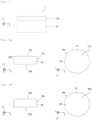
- the present invention relates to a method of manufacturing a composite structure 1 comprising a thin layer 100 of a first monocrystalline material placed on a support substrate 20 ( figure 1 ).
- the first material could in particular be silicon carbide (SiC), gallium arsenide (GaAs), indium phosphide (InP), gallium nitride (GaN), aluminum nitride (AlN), silicon germanium (SiGe), silicon (Si), germanium (Ge) or others.
- SiC silicon carbide
- GaAs gallium arsenide
- InP indium phosphide
- GaN gallium nitride
- AlN aluminum nitride
- SiGe silicon germanium
- Si silicon germanium
- the method firstly comprises a step a) of supplying a donor substrate 10 composed of the first monocrystalline material ( figure 2a ).
- the thin layer 100 of the composite structure 1 will be formed, at the end of the process of the present invention, from the donor substrate 10: thus, the crystallographic orientation, the quality crystalline as well as the doping level of the donor substrate 10 are chosen to meet the required specifications of the components, for example vertical, intended to be produced on the thin layer 100.
- a donor substrate 10 in c-SiC could be of polytype 4H or 6H, having a disorientation ("offcut") less than 4.0° relative to the crystallographic axis ⁇ 11-20> ⁇ 0.5°, and a density of crossing dislocations (“Micropipes”) less than or equal to 5/cm 2 , or even less than 1/cm 2 .
- Doped with type N (nitrogen) it has a resistivity preferably between 0.015 ohm.cm and 0.030 ohm.cm.
- BPD basal plane dislocation density
- the donor substrate 10 in c-SiC may comprise an initial substrate 10' and a surface layer 110 on the side of its front face 10a, produced for example by epitaxy, and having the properties required for the future thin layer 100; the latter will be formed, at the end of the process of the present invention, from said surface layer 110 ( Figure 3 ).
- a density of BPD type defects in the surface layer 110 lower than that of the initial substrate 10', and advantageously less than 5/cm 2 , or even less than 1/cm 2 .
- a donor substrate 10 in c-InP may have a disorientation ("offcut") of 2°.
- the donor substrate 10 is preferably in the form of a circular plate with a diameter of 100mm or 150mm or even 200mm and a thickness typically between 300 and 800 microns. It has a front face 10a, a rear face 10b and a edge 10c forming its circular perimeter. Roughness of surface of the front face 10a is advantageously chosen less than 1 nm Ra, average roughness measured by atomic force microscopy (AFM) on a scan of 20 microns x 20 microns.
- AFM atomic force microscopy
- the donor substrate 10 usually comprises a flat 11 or a notch (called “notch” according to Anglo-Saxon terminology) fitted at the level of its edge 10c.
- the flat 11 or the notch identifies a particular crystallographic axis, contained in the plane (x,y) of the front face 10a: for a c-SiC substrate, the crystallographic axis (11-20) is for example parallel to the flat 11. The precision of this identification is nevertheless low, since the flat 11 guarantees the direction of the crystallographic axis to +/-1°.
- the donor substrate 10 may include one or more micrometric or millimetric patterns produced by known techniques of lithography, engraving and deposition, on its front face 10a or on its rear face 10b, and capable of indicating a crystallographic direction particular.
- the method also comprises a step b) of providing a support substrate 20 ( figure 2b ).
- a support substrate 20 ( figure 2b ).
- the latter can be chosen from any material compatible with the microelectronic processes usually used to develop components based on the first material.
- the support substrate 20 could therefore be made of silicon, silicon carbide, gallium arsenide, indium phosphide, etc.
- the support substrate 20 is poly-crystalline silicon carbide (p-SiC) or silicon carbide monocrystalline. In the latter case, a higher level of defects and dislocations can be tolerated than for the donor substrate 10 (and the thin layer 100 which will result).
- the support substrate 20 has a resistivity of between 0.015 ohm.cm and 0.030 ohm.cm to meet the electrical conduction requirements of the vertical components likely to be produced on the future composite structure 1.
- the support substrate 20 is preferably in the form of a circular plate with a diameter of 100mm or 150mm or even 200mm and a thickness typically between 300 and 800 microns. It has a front face 20a, a rear face 20b and a edge 20c forming its circular perimeter.
- the surface roughness of the front face 20a is advantageously chosen less than 1 nm Ra, as for the donor substrate 10.
- the support substrate 20 generally comprises an alignment pattern 21 (hereinafter called first alignment pattern 21), which is arranged on one of the front 20a and rear 20b faces or on the edge 20c.
- first alignment pattern 21 is a flat area provided at the level of the edge 20c of the support substrate 20.
- the first alignment pattern may consist of a notch also provided at the level of the edge 20c.
- the first alignment pattern 21 may consist of one or more micrometric or millimetric patterns produced by known techniques of lithography, engraving and deposition, on the front face 20a or on the rear face 20b of the support substrate 20 , and likely to indicate a particular direction or to serve as a reference to align levels of subsequent lithographic masks.
- the first alignment pattern 21 identifies a crystallographic axis contained in the plane (x,y) parallel to the front face 20a of the substrate 20, as explained previously for the donor substrate 10, with an accuracy of +/-1°.
- the method according to the invention then comprises a step c) of heat treatment applied to the donor substrate 10 and optionally to the support substrate 20, under a controlled atmosphere and at a temperature capable of causing a surface reorganization on at least one of the faces of the treated substrate.
- the surface reorganization gives rise to the formation of steps ("step bunching" according to Anglo-Saxon terminology) parallel to each other and having a nanometric amplitude, for example of the order of a few nanometers up to 500nm.
- the heat treatment of step c) is applied to the donor substrate 10 (and potentially to the support substrate 20, if it too is made of silicon carbide) at a temperature greater than or equal to 1500 °C, preferably greater than or equal to 1600°C.
- the temperature is typically chosen between 1500°C and 1800°C, for example 1700°C, and the atmosphere is advantageously neutral or reducing, based on argon and/or a mixture of argon and approximately 2 % hydrogen.
- a temperature is sufficiently high for at least one compound of silicon carbide (in this case silicon) to be able to exo-diffuse.
- such heat treatment causes a surface reorganization on at least one of the faces of said substrate giving rise to the formation of parallel steps between them and having a nanometric amplitude, of the order of a few nanometers up to 'at 500nm.
- the heat treatment temperature of step c) is chosen greater than or equal to 630° C., under an arsine atmosphere; the exo-diffusion of arsenic causes the expected surface reorganization.
- the heat treatment temperature of step c) is chosen greater than or equal to 600° C., under a phosphine atmosphere; it is then the phosphorus which tends to exo-diffuse and the surface reorganization in the form of steps can take place.
- step c the application of the heat treatment of step c), under a controlled atmosphere allows a reorganization of the surface in the form of steps and avoids (or limits) the appearance of holes (“etch pits” according to Anglo-Saxon terminology).
- the donor substrate 10 has steps 13 (hereinafter called first steps) on its front face 10a and/or on its rear face 10b, all parallel to a main axis P1 (called first axis main axis): this main axis P1 indicates a well-defined crystallographic axis, depending on the nature of the first material.
- the main axis P1 is parallel to the crystallographic axis (1-100).
- the presence of the first steps 13, on the front face 10a and/or on the rear face 10b of the donor substrate 10 can constitute a registration mark 12 indicating the main axis P1, and therefore the associated crystallographic axis in the plane ( x,y).
- the registration mark 12 is formed by at least one mark defined by conventional photolithography and engraving techniques, on the front face 10a of the donor substrate 10, from the first steps 13 ( figure 4 ) .
- At least one mark is defined on the rear face 10b of the donor substrate 10 from the first steps 13, thus forming the registration mark 12 at the level of the rear face 10b.
- This option is advantageous in that it avoids local structuring of the front face 10a of the donor substrate 10, which is favorable for a subsequent assembly step.
- steps 23 are thus generated on its front face 20a and/ or on its rear face 20b, all parallel to a main axis P2 (called second main axis): this main axis P2 indicates a well-defined crystallographic axis of the support substrate 20.
- a heat treatment step c different (in terms of temperature and/or atmosphere) from that applied to the donor substrate 10, could be applied to the support substrate 20, if it is composed of a monocrystalline material different from the first material.
- the conditions of step c) would then be defined so as to cause the desired surface reorganization on the support substrate 20.
- the presence of the second steps 23, on the front face 20a and/or on the rear face 20b of the support substrate 20 can constitute a second alignment pattern 22 indicating the main axis P2, and consequently the crystallographic axis associated in the (x,y) plane.
- the second alignment pattern 22 is formed by at least one pattern (defined by conventional photolithography and engraving techniques), on the face front 20a of the support substrate 20, from the second steps 23 ( figure 4 ).
- At least one pattern is defined on the rear face 20b of the support substrate 20 from the second steps 23, thus forming the second alignment pattern 22 at the level of the rear face 20b.
- the c-SiC of polytype 4H is polar and can present, as a front face, an Si face or a C face: taking into account the different energy levels of these two faces, the surface reconstruction of a face Si will generate many more steps, of greater amplitude, than the reconstruction of a face C, under certain annealing conditions.
- the method then comprises a step d) of assembling the donor substrate 10 and the support substrate 20, via their respective front faces 10a, 20a.
- This step includes bringing the two substrates 10,20 into intimate contact, to effect direct bonding, by molecular adhesion.
- bonding requires that the assembled surfaces be cleaned beforehand, to remove contamination (particulate, organic, etc.), and potentially activated, to favor chemical surface endings favorable to the propagation of the bonding wave and the good performance of the bonding interface.
- an optical alignment is carried out between a registration mark 12 indicating the first main axis P1 on the donor substrate 10 and at least one alignment pattern 21,22 of the support substrate 20.
- the alignment between the registration mark 12 and the alignment pattern 21,22 is aimed with a precision better than +/-0 .1°, or even better than +/-0.05°.
- the objective of this alignment is to ensure that the first main axis P1 (corresponding to a particular crystallographic axis of the donor substrate 10, and therefore of the thin layer 100 which will result from it) is precisely identified by the first 21 or the second 22 alignment pattern of the support substrate 20.
- optical alignment can be carried out indifferently between marks or patterns arranged on the front faces 10a, 20, the rear faces 10b, 20b or the edges 10c, 20c of the donor 10 and support 20 substrates.
- the optical alignment is carried out between the registration mark 12, whatever it may be, and the first alignment pattern 21 of the support substrate 20 ( figure 2d ).
- the support substrate 20 it is not necessary for the support substrate 20 to have undergone heat treatment step c), because a second alignment pattern 22, based on the second steps 23 is not used.
- the first variant is advantageously implemented when the support substrate 20 comprises an amorphous or polycrystalline material, for example p-SiC.
- the optical alignment is carried out between the registration mark 12, whatever it may be, and the second alignment pattern 22 of the support substrate 20, whatever it may be ( Figure 5 ).
- the heat treatment of step c) was applied to the support substrate 20, so as to generate the second steps 23 required to form a second alignment pattern 22.
- This second variant is advantageously implemented when the support substrate 20 comprises a single crystal material, for example c-SiC. It is also preferred in the case where the future composite structure 1 is intended for the development of vertical components.
- Step d) of assembling the substrates 10,20 may include a surface treatment to smooth one or other of the front faces 10a, 20a of the donor substrates 10 and support 20, prior to their bringing into contact. Indeed, the presence of steps 13 on at least the front face 10a of the donor substrate 10 can affect the quality of the direct bonding.
- the principles mentioned below with reference to the donor substrate 10 apply in a similar manner when second steps 23 are present on the front face of the support substrate 20.
- mechanical-chemical polishing of the front face 10a of the donor substrate 10 can for example be carried out before the optical alignment and the bringing into contact of the two substrates 10,20.
- the polishing having the consequence of making the first steps 13 disappear it is necessary that a registration mark 12 on the donor substrate 10 (or a second alignment pattern 22 on the support substrate 20) has been produced at from steps 13 before said polishing.
- steps 13 present on the rear face 10b of the donor substrate 10 can be used to develop a registration mark 12 or directly for optical alignment.
- assembly step d) may also include the deposition of an intermediate layer on the front face 10a of the donor substrate 10 and/or on the front face 20a of the support substrate 20.
- the intermediate layer can be an insulating or electrically conductive layer, for example metallic, depending on the type of component which will be produced on the composite structure 1 at the end of the process according to the invention.
- the insulating layer may comprise a material chosen from silicon oxide, silicon nitride, etc.
- the intermediate layer can also be smoothed, for example by mechanical-chemical polishing, to facilitate direct bonding of the substrates 10,20.
- the steps 13,23 on the front faces 10a,20a of the donor 10 and support 20 substrates are thus encapsulated and do not hinder assembly.
- the contacting of the substrates 10,20 can be done under ambient atmosphere or under controlled atmosphere, for example under neutral gas and/or under vacuum. It can also be operated at a controlled temperature, for example between 20°C and 300°C.
- the contacting of the substrates 10,20 is accompanied by the propagation of a wave of bonding, creating a bonding interface 30 and resulting in a bonded assembly 1' ( figure 2d ).
- the manufacturing method according to the invention finally comprises a step e) of transferring a thin layer 100 from the donor substrate 10 onto the support substrate 20 ( figure 2e ).
- the transfer of the thin layer 100 is carried out by thinning the rear face 10b of the donor substrate 10, up to the desired thickness of the thin layer 100.
- thinning can for example implement conventional techniques of mechanical rectification (“grinding” according to Anglo-Saxon terminology), wet or dry chemical etching and/or mechanical-chemical polishing, alternating with cleaning sequences.
- One (or more) thermal treatment(s) may be applied to consolidate the bonding interface or to improve the crystalline and/or surface quality of the thin layer 100.
- the transfer of the thin layer 10 is carried out by the Smart Cut TM process.
- the manufacturing method according to the invention comprises, before the assembly step, a step of forming a buried fragile plane 15 in the donor substrate 10, delimiting the thin layer 100 between said buried fragile plane 15 and the front face 10a of the donor substrate 10 ( figure 6a ).
- a step of ion implantation of light species is carried out up to a determined depth in the donor substrate 10.
- the light species implanted are preferably hydrogen, helium or a co-implantation of these two species. These light species will form, around the determined depth, microcavities distributed in a thin layer parallel to the free surface of the donor substrate 10, or parallel to the plane (x,y) on the figure 6a . We call this thin layer the fragile buried plane 15, for the sake of simplification.
- the implantation energy of the light species is chosen so as to reach the determined depth in the donor substrate 10, said depth corresponding to a targeted thickness of the thin layer 10 after transfer.
- hydrogen ions will be implanted at an energy between 10 keV and 250 keV (or even up to 500 keV), and at a dose between 5 E 16/cm2 and 1 E 17/cm2, to delimit a thin layer 10 of the order of 100 to 1500 nm.
- a protective layer may be deposited on the front face 10a of the donor substrate 10, prior to the ion implantation step. This protective layer can be composed of a material such as silicon oxide or silicon nitride.
- transfer step e) comprises a separation along the buried fragile plane 15, to form the composite structure 1 comprising the thin layer 100 placed on the support substrate 20 on the one hand, and the remainder 10'' of the substrate donor on the other hand.
- the separation can be induced by applying a heat treatment at a temperature typically between 200°C and 1000°C, for a few minutes to a few hours; in particular, a temperature between 800°C and 1000°C in the case of a first c-SiC material, or between 200°C and 300°C in the case of a first c-GaAs material, or still around 300°C in the case of a first c-InP material.
- a heat treatment at a temperature typically between 200°C and 1000°C, for a few minutes to a few hours; in particular, a temperature between 800°C and 1000°C in the case of a first c-SiC material, or between 200°C and 300°C in the case of a first c-GaAs material, or still around 300°C in the case of a first c-InP material.
- separation can be induced by application of localized stress, or by a combination of heat treatment and mechanical stress.
- the free face of the thin layer 10 typically has a roughness of between 3 and 6 nm Ra (AFM - scan 20 microns x 20 microns).
- the goal for subsequent component manufacturing is to have a roughness below 1 nm Ra.
- the manufacturing process can include finishing steps applied to the composite structure 1. These finishing steps aim in particular to improve the roughness of the free surface of the thin layer 100 (face before 1a of the composite structure 1).
- finishing steps may in particular use known mechanical-chemical polishing techniques, applied to the front face 1a. They can also include heat treatments aimed at consolidating the bonding interface 30 or even improving the crystalline and/or surface quality of the thin layer 100.
- the identification mark 12 of the donor substrate 10 is either absent from the composite structure 1 (in particular if it was located on the face rear 10b of the donor substrate 10), either inconspicuous or degraded (if it was located on the front face 10a or the edge 10c of the donor substrate 10).
- the donor substrate 10 provided in step a) of the manufacturing process is a c-SiC wafer, of polytype 4H, with an orientation of 4.0° relative to the axis ⁇ 11 -20> ⁇ 0.5°, diameter 150mm and thickness 350um.
- the front face 10a of the donor substrate 10 is a face of type C (carbon), while its rear face 10b is of type Si (silicon).
- the donor substrate 10 may comprise a flat 11 arranged at its edge 10c and indicating to within +/-1°, the crystallographic direction (1-100) contained in the plane (x,y) of the front face 10a of said substrate 10.
- the support substrate 20 provided in step b) of the manufacturing process is a c-SiC wafer, of polytype 4H, of orientation 4.0° relative to the axis ⁇ 11-20> ⁇ 0.5°, of diameter 150mm and thickness 350pm.
- the support substrate 20 comprises a flat 21 arranged at its edge 20c and indicating the crystallographic direction (1-100) contained in the plane (x,y) of the front face 20a of said substrate 20.
- the front face 20a is of the type If and the rear face 20b is type C.
- a classic cleaning sequence is carried out on the substrates 10,20 prior to heat treatment step c).
- the heat treatment at 1700°C under argon or under argon combined with 2% hydrogen is then applied to the two substrates 10,20, causing the appearance of first steps 13 on the faces 10a, 10b of the donor substrate 10 and second steps 23 on the faces 20a, 20b of the support substrate 20.
- the first steps 13 on the donor substrate 10 are of greater amplitude on its rear face 10b (face Si) than on its front face 10a (face C); and the second steps 23 on the support substrate 20 are of greater amplitude on its front face 20a (face Si) than on its rear face (face C).
- the donor substrate 10 and the support substrate 20 being of the same nature and the same crystal orientation, the first main axis P1 and the second main axis P2, respectively parallel to the first steps 13 and to the second steps 23 correspond to the same crystallographic axis (1 -100).
- a registration mark 12 is defined on said rear face 10b.
- a second alignment pattern 22 is defined on the rear face 20b of said substrate 20.
- the mark 12 and the second pattern 22 are made so as to indicate precisely the direction respectively of the first (P1) and the second (P2) main axis. They can each consist of two alignment crosses, arranged at the edge of the associated substrate.
- Hydrogen ions are implanted at an energy of 60keV and a dose of 6 E 16 H+/cm 2 , through the front face 10a of the donor substrate 10.
- the donor substrate 10 may include a protective layer at the level of its front face 10a, through which the ions are implanted.
- a buried fragile plane 15 is created at a depth of approximately 500 nm in the donor substrate 10.
- Assembly step d) includes mechanical-chemical polishing of the front faces 10a, 20a of the substrates 10,20, to eliminate the steps 13,23 generated during step c) and restore a good surface condition and a roughness less than 0.2 nm rms, favorable to quality assembly. Note that the aforementioned protective layer, if present, will be removed prior to polishing.
- the substrates 10,20 are then introduced into bonding equipment equipped with an alignment module allowing optical alignment to better than +/-0.1°.
- the registration mark 12 on the rear face 10b of the donor substrate 10 and the second alignment pattern 22 on the rear face 20b of the support substrate 20 are used for this optical alignment between the substrates.
- the crystallographic axes (1-100) of the two substrates 10,20 will thus be aligned to better than +/- 0.1°.
- the crystallographic axis (1-100) of the donor substrate 10 may be offset relative to the crystallographic axis (1-100) of the support substrate 20 by 0.1° at most.
- the assembly then takes place by bringing the two substrates into contact, aligned with each other, under a neutral atmosphere (Ar or N) and under vacuum ( ⁇ 1 E- 8 Pa).
- Transfer step e) is carried out by applying annealing at 950°C for 30 min: a spontaneous separation along the buried fragile plane takes place, giving rise to the composite structure 1 and the remainder 10" of the substrate giver.
- the second alignment pattern 22, present on the rear face 20b of the support substrate 20 (which is also the rear face of the composite structure 1), indicates precisely, to within +/-0.1° (or even better), the direction of the crystallographic axis (1-100) of the thin layer 100 and can be easily used when producing components on said layer 100 of the composite structure 1.
Landscapes
- Crystals, And After-Treatments Of Crystals (AREA)
- Chemical & Material Sciences (AREA)
- Crystallography & Structural Chemistry (AREA)
Claims (10)
- Verfahren zum Herstellen einer Verbundstruktur (1), umfassend eine dünne Schicht (100) aus einem ersten monokristallinen Material, die auf einem Trägersubstrat (20) angeordnet ist, das Verfahren umfassend:- einen Schritt a) eines Bereitstellens eines Donorsubstrats (10), das aus dem ersten monokristallinen Material besteht, das eine Vorderseite (10a) und eine Rückseite (10b) aufweist,- einen Schritt b) des Bereitstellens eines Trägersubstrats (20), das eine Vorderseite (20a), eine Rückseite (20b), einen Rand (20c) und ein erstes Ausrichtungsmuster (21) auf der einen der Seiten oder auf dem Rand aufweist,- einen Schritt c) eines Wärmebehandelns, das auf mindestens ein Donorsubstrat (10) unter kontrollierter Atmosphäre und bei einer Temperatur angewendet wird, die geeignet ist, um eine Oberflächenneuordnung auf mindestens einer der Seiten (10a, 10b) des Substrats (10) zu bewirken, wobei die Oberflächenneuordnung die Ausbildung von ersten Stufen (13) mit Nanometeramplitude verursacht, die parallel zu einer ersten Hauptachse (P1) sind,- einen Schritt d) eines Verbindens des Donorsubstrats (10) und des Trägersubstrats (20), umfassend vor dem Inkontaktbringen der Substrate (10, 20) eine optische Ausrichtung besser als +/-01°, zwischen einer Einstellmarke (12), die die erste Hauptachse (P1) auf dem Donorsubstrat (10) angibt, und mindestens einem Ausrichtungsmuster (21,22) des Trägersubstrats (20),- einen Schritt e) eines Übertragens einer dünnen Schicht (100), die von dem Donorsubstrat (10) stammt, auf das Trägersubstrat (20).
- Herstellungsverfahren nach dem vorstehenden Anspruch, wobei:- das erste Ausrichtungsmuster (21) des Trägersubstrats (20) eine Abflachung oder eine Kerbe ist, die an dem Rand (20c) eingerichtet ist, und- die optische Ausrichtung bei dem Verbindungsschritt das erste Ausrichtungsmuster (21) verwendet.
- Herstellungsverfahren nach einem der vorstehenden Ansprüche, wobei das erste Material Siliciumcarbid ist und wobei die Temperatur der Wärmebehandlung von dem Schritt c) höher als oder gleich 1500 °C, vorzugsweise höher als oder gleich 1600 °C ist.
- Herstellungsverfahren nach dem vorstehenden Anspruch, wobei:- das Trägersubstrat (20) aus monokristallinem Siliciumcarbid ist,- der Wärmebehandlungsschritt auch auf das Trägersubstrat (20) angewendet wird und eine Oberflächenneuordnung auf mindestens einer der Seiten (20a, 20b) des Substrats bewirkt, wobei die Oberflächenneuordnung die Ausbildung von zweiten Stufen (23) mit Nanometeramplitude verursacht, die parallel zu einer zweiten Hauptachse (P2) sind,- ein zweites Ausrichtungsmuster (22) auf dem Trägersubstrat (20) durch die zweiten Gänge (23) selbst ausgebildet ist, wobei mindestens ein Muster durch Fotolithographie und Ätzen auf der Vorderseite (20a) des Trägersubstrats (20) aus den zweiten Stufen (23) oder durch mindestens ein Muster, das durch Fotolithographie und Ätzen auf der Rückseite (20b) des Trägersubstrats (20) aus den zweiten Stufen (23) definiert ist,- die optische Ausrichtung bei dem Verbindungsschritt das zweite Ausrichtungsmuster (22) verwendet.
- Herstellungsverfahren nach einem der Ansprüche 1 und 2, wobei das erste Material Galliumarsenid ist und wobei die Temperatur der Wärmebehandlung von dem Schritt c) größer als oder gleich 630 °C ist.
- Herstellungsverfahren nach einem der Ansprüche 1 und 2, wobei das erste Material Indiumphosphid ist und wobei die Temperatur der Wärmebehandlung von Schritt c) größer als oder gleich 600 °C ist.
- Herstellungsverfahren nach einem der vorstehenden Ansprüche, wobei die Einstellmarke (12) durch die ersten Gänge (13) selbst ausgebildet wird, durch mindestens eine Marke, die durch Fotolithographie und Ätzen auf der Vorderseite (10a) des Donorsubstrats (10) aus den ersten Stufen (13) definiert ist, oder durch mindestens eine Marke, die durch Fotolithographie und Ätzen auf der Rückseite (10b) des Donorsubstrats (10) aus den ersten Stufen (13) definiert ist.
- Herstellungsverfahren nach einem der vorstehenden Ansprüche, wobei der Verbindungsschritt ein mechanisch-chemisches Polieren der Vorderseite (10a) des Donorsubstrats (10) und/oder der Vorderseite (20a) des Trägersubstrats (20) vor dem Inkontaktbringen der zwei Substrate (10, 20) umfasst.
- Herstellungsverfahren nach einem der vorstehenden Ansprüche, wobei der Verbindungsschritt das Abscheiden einer Zwischenschicht auf die Vorderseite (10a) des Donorsubstrats (10) und/oder auf die Vorderseite (20a) des Trägersubstrats (20) im Vorfeld des Inkontaktbringens der zwei Substrate (10, 20) umfasst.
- Herstellungsverfahren nach einem der vorstehenden Ansprüche, umfassend:- vor dem Verbindungsschritt, einen Schritt des Ausbildens einer eingegrabenen spröden Ebene (15) in dem Donorsubstrat (10), die die dünne Schicht (100) zwischen der eingegrabenen spröden Ebene (15) und der Vorderseite (10a) des Donorsubstrats (10) begrenzt,- während des Übertragungsschritts, eine Trennung entlang der eingegrabenen spröden Ebene (15) zum Ausbilden der Verbundstruktur (1), umfassend einerseits die dünne Schicht(100), die auf dem Trägersubstrat (20) angeordnet ist, und andererseits den Rest (10") des Donorsubstrats.
Applications Claiming Priority (2)
| Application Number | Priority Date | Filing Date | Title |
|---|---|---|---|
| FR1915720A FR3105876B1 (fr) | 2019-12-30 | 2019-12-30 | Procédé de fabrication d’une structure composite comprenant une couche mince en SiC monocristallin sur un substrat support |
| PCT/FR2020/052451 WO2021136894A1 (fr) | 2019-12-30 | 2020-12-15 | Procede de fabrication d'une structure composite comprenant une couche mince monocristalline sur un substrat support |
Publications (2)
| Publication Number | Publication Date |
|---|---|
| EP4085478A1 EP4085478A1 (de) | 2022-11-09 |
| EP4085478B1 true EP4085478B1 (de) | 2023-10-25 |
Family
ID=69903605
Family Applications (1)
| Application Number | Title | Priority Date | Filing Date |
|---|---|---|---|
| EP20845581.6A Active EP4085478B1 (de) | 2019-12-30 | 2020-12-15 | Verfahren zur herstellung einer verbundstruktur mit einer dünnen monokristallinen schicht auf einem trägersubstrat |
Country Status (6)
| Country | Link |
|---|---|
| US (1) | US12087631B2 (de) |
| EP (1) | EP4085478B1 (de) |
| JP (1) | JP7637679B2 (de) |
| FR (1) | FR3105876B1 (de) |
| TW (1) | TWI833057B (de) |
| WO (1) | WO2021136894A1 (de) |
Families Citing this family (2)
| Publication number | Priority date | Publication date | Assignee | Title |
|---|---|---|---|---|
| WO2024004314A1 (ja) * | 2022-06-30 | 2024-01-04 | 日本碍子株式会社 | 複合基板および13族元素窒化物エピタキシャル成長用基板 |
| TWI912574B (zh) * | 2023-01-10 | 2026-01-21 | 中國砂輪企業股份有限公司 | 複合式基板及複合式基板之製備方法 |
Family Cites Families (9)
| Publication number | Priority date | Publication date | Assignee | Title |
|---|---|---|---|---|
| US5236118A (en) * | 1992-05-12 | 1993-08-17 | The Regents Of The University Of California | Aligned wafer bonding |
| FR2819099B1 (fr) * | 2000-12-28 | 2003-09-26 | Commissariat Energie Atomique | Procede de realisation d'une structure empilee |
| US6699770B2 (en) * | 2001-03-01 | 2004-03-02 | John Tarje Torvik | Method of making a hybride substrate having a thin silicon carbide membrane layer |
| FR2826378B1 (fr) | 2001-06-22 | 2004-10-15 | Commissariat Energie Atomique | Structure composite a orientation cristalline uniforme et procede de controle de l'orientation cristalline d'une telle structure |
| US6784071B2 (en) * | 2003-01-31 | 2004-08-31 | Taiwan Semiconductor Manufacturing Company, Ltd. | Bonded SOI wafer with <100> device layer and <110> substrate for performance improvement |
| FR2982071B1 (fr) | 2011-10-27 | 2014-05-16 | Commissariat Energie Atomique | Procede de lissage d'une surface par traitement thermique |
| JP2016172662A (ja) | 2015-03-17 | 2016-09-29 | 富士電機株式会社 | SiC基板の製造方法 |
| EP3584821B1 (de) | 2017-02-16 | 2025-03-12 | Shin-Etsu Chemical Co., Ltd. | Halbleiterlaminatsubstrat aus verbundwerkstoff, verfahren zur herstellung davon und halbleiterelement |
| NL2018856B1 (en) * | 2017-05-05 | 2018-11-14 | Suss Microtec Lithography Gmbh | Method and device for aligning a first substrate with a second substrate |
-
2019
- 2019-12-30 FR FR1915720A patent/FR3105876B1/fr active Active
-
2020
- 2020-12-15 JP JP2022527974A patent/JP7637679B2/ja active Active
- 2020-12-15 WO PCT/FR2020/052451 patent/WO2021136894A1/fr not_active Ceased
- 2020-12-15 US US17/757,797 patent/US12087631B2/en active Active
- 2020-12-15 EP EP20845581.6A patent/EP4085478B1/de active Active
- 2020-12-28 TW TW109146402A patent/TWI833057B/zh active
Also Published As
| Publication number | Publication date |
|---|---|
| EP4085478A1 (de) | 2022-11-09 |
| JP7637679B2 (ja) | 2025-02-28 |
| US20220359293A1 (en) | 2022-11-10 |
| TWI833057B (zh) | 2024-02-21 |
| JP2023508834A (ja) | 2023-03-06 |
| FR3105876A1 (fr) | 2021-07-02 |
| FR3105876B1 (fr) | 2021-11-26 |
| TW202139260A (zh) | 2021-10-16 |
| US12087631B2 (en) | 2024-09-10 |
| WO2021136894A1 (fr) | 2021-07-08 |
Similar Documents
| Publication | Publication Date | Title |
|---|---|---|
| FR3103961A1 (fr) | Procede de fabrication d’une structure composite comprenant une couche mince en sic monocristallin sur un substrat support en sic | |
| EP4008020B1 (de) | Verfahren zur herstellung einer verbundstruktur mit einer dünnen schicht aus monokristallinem sic auf einem trägersubstrat aus polykristallinem sic | |
| EP4128329B1 (de) | Verfahren zur herstellung einer verbundstruktur mit einer dünnen schicht aus monokristallinem sic auf einem trägersubstrat aus sic | |
| EP4128328B1 (de) | Verfahren zur herstellung einer verbundstruktur mit einer dünnen schicht aus monokristallinem sic auf einem trägersubstrat aus sic | |
| EP2031654A2 (de) | Verfahren zur Herstellung einer Struktur für Epitaxie ohne Ausschlusszone | |
| FR2817395A1 (fr) | Procede de fabrication d'un substrat notamment pour l'optique, l'electronique ou l'optoelectronique et substrat obtenu par ce procede | |
| EP4066275B1 (de) | Verfahren zum herstellen einer verbundstuktur mit einer dünnen schicht aus einkristallinem sic auf einem sic-trägersubstrat | |
| EP4162522B1 (de) | Abnehmbares temporäres substrat mit sehr hohen temperaturen und verfahren zur übertragung einer arbeitsschicht von diesem substrat | |
| EP4264659B1 (de) | Verfahren zur herstellung einer halbleiterstruktur mit einem agglomerat-haltigen grenzflächenbereich | |
| EP4085478B1 (de) | Verfahren zur herstellung einer verbundstruktur mit einer dünnen monokristallinen schicht auf einem trägersubstrat | |
| EP4128330B1 (de) | Verfahren zum produzieren einer gestapelten struktur | |
| EP3766094B1 (de) | Verfahren zur herstellung einer dünnschicht aus einem ferroelektrikum auf alkalibasis | |
| EP4413613B1 (de) | Verfahren zur herstellung einer verbundstruktur mit einer dünnschicht aus monokristallinem sic auf einem trägersubstrat aus polykristallinem sic | |
| WO2026041589A1 (fr) | Procédé de fabrication d'une structure composite incluant une couche mince monocristalline transférée sur un substrat support | |
| WO2025186045A1 (fr) | Procédé de préparation d'un substrat support en matériau polycristallin et procédé de fabrication d'une structure composite incluant ledit substrat support | |
| WO2025103850A1 (fr) | Procédé de fabrication d'une couche en carbure de silicium homoépitaxiée, permettant de limiter la formation de défauts de type bpd, et structure composite associee | |
| WO2025186046A1 (fr) | Procédé de préparation d'un substrat support en matériau polycristallin et procédé de fabrication d'une structure composite incluant ledit substrat support | |
| EP4409621A1 (de) | Verfahren zur herstellung einer verbundstruktur mit einer dünnschicht aus monokristallinem sic auf einem trägersubstrat aus polykristallinem sic | |
| WO2026061720A1 (fr) | Procédé de fabrication d'une structure semi-conductrice à base de carbure de silicium et structure composite intermédiaire | |
| FR3165752A1 (fr) | Procédé de fabrication d’une structure composite incluant une couche mince monocristalline transférée sur un substrat support | |
| FR3151939A1 (fr) | Procédé de fabrication d’une couche contrainte | |
| EP4315396A1 (de) | Verfahren zur herstellung einer verbundstruktur mit einer dünnen einkristallinen halbleiterschicht auf einem trägersubstrat |
Legal Events
| Date | Code | Title | Description |
|---|---|---|---|
| STAA | Information on the status of an ep patent application or granted ep patent |
Free format text: STATUS: UNKNOWN |
|
| STAA | Information on the status of an ep patent application or granted ep patent |
Free format text: STATUS: THE INTERNATIONAL PUBLICATION HAS BEEN MADE |
|
| PUAI | Public reference made under article 153(3) epc to a published international application that has entered the european phase |
Free format text: ORIGINAL CODE: 0009012 |
|
| STAA | Information on the status of an ep patent application or granted ep patent |
Free format text: STATUS: REQUEST FOR EXAMINATION WAS MADE |
|
| 17P | Request for examination filed |
Effective date: 20220525 |
|
| AK | Designated contracting states |
Kind code of ref document: A1 Designated state(s): AL AT BE BG CH CY CZ DE DK EE ES FI FR GB GR HR HU IE IS IT LI LT LU LV MC MK MT NL NO PL PT RO RS SE SI SK SM TR |
|
| DAV | Request for validation of the european patent (deleted) | ||
| DAX | Request for extension of the european patent (deleted) | ||
| GRAP | Despatch of communication of intention to grant a patent |
Free format text: ORIGINAL CODE: EPIDOSNIGR1 |
|
| STAA | Information on the status of an ep patent application or granted ep patent |
Free format text: STATUS: GRANT OF PATENT IS INTENDED |
|
| INTG | Intention to grant announced |
Effective date: 20230712 |
|
| RIN1 | Information on inventor provided before grant (corrected) |
Inventor name: GAUDIN, GWELTAZ |
|
| GRAS | Grant fee paid |
Free format text: ORIGINAL CODE: EPIDOSNIGR3 |
|
| GRAA | (expected) grant |
Free format text: ORIGINAL CODE: 0009210 |
|
| STAA | Information on the status of an ep patent application or granted ep patent |
Free format text: STATUS: THE PATENT HAS BEEN GRANTED |
|
| AK | Designated contracting states |
Kind code of ref document: B1 Designated state(s): AL AT BE BG CH CY CZ DE DK EE ES FI FR GB GR HR HU IE IS IT LI LT LU LV MC MK MT NL NO PL PT RO RS SE SI SK SM TR |
|
| REG | Reference to a national code |
Ref country code: GB Ref legal event code: FG4D Free format text: NOT ENGLISH |
|
| REG | Reference to a national code |
Ref country code: CH Ref legal event code: EP |
|
| REG | Reference to a national code |
Ref country code: DE Ref legal event code: R096 Ref document number: 602020020000 Country of ref document: DE |
|
| REG | Reference to a national code |
Ref country code: IE Ref legal event code: FG4D Free format text: LANGUAGE OF EP DOCUMENT: FRENCH |
|
| REG | Reference to a national code |
Ref country code: LT Ref legal event code: MG9D |
|
| REG | Reference to a national code |
Ref country code: NL Ref legal event code: MP Effective date: 20231025 |
|
| REG | Reference to a national code |
Ref country code: AT Ref legal event code: MK05 Ref document number: 1625563 Country of ref document: AT Kind code of ref document: T Effective date: 20231025 |
|
| PG25 | Lapsed in a contracting state [announced via postgrant information from national office to epo] |
Ref country code: NL Free format text: LAPSE BECAUSE OF FAILURE TO SUBMIT A TRANSLATION OF THE DESCRIPTION OR TO PAY THE FEE WITHIN THE PRESCRIBED TIME-LIMIT Effective date: 20231025 |
|
| PG25 | Lapsed in a contracting state [announced via postgrant information from national office to epo] |
Ref country code: GR Free format text: LAPSE BECAUSE OF FAILURE TO SUBMIT A TRANSLATION OF THE DESCRIPTION OR TO PAY THE FEE WITHIN THE PRESCRIBED TIME-LIMIT Effective date: 20240126 |
|
| PG25 | Lapsed in a contracting state [announced via postgrant information from national office to epo] |
Ref country code: IS Free format text: LAPSE BECAUSE OF FAILURE TO SUBMIT A TRANSLATION OF THE DESCRIPTION OR TO PAY THE FEE WITHIN THE PRESCRIBED TIME-LIMIT Effective date: 20240225 |
|
| PG25 | Lapsed in a contracting state [announced via postgrant information from national office to epo] |
Ref country code: LT Free format text: LAPSE BECAUSE OF FAILURE TO SUBMIT A TRANSLATION OF THE DESCRIPTION OR TO PAY THE FEE WITHIN THE PRESCRIBED TIME-LIMIT Effective date: 20231025 |
|
| PG25 | Lapsed in a contracting state [announced via postgrant information from national office to epo] |
Ref country code: AT Free format text: LAPSE BECAUSE OF FAILURE TO SUBMIT A TRANSLATION OF THE DESCRIPTION OR TO PAY THE FEE WITHIN THE PRESCRIBED TIME-LIMIT Effective date: 20231025 |
|
| PG25 | Lapsed in a contracting state [announced via postgrant information from national office to epo] |
Ref country code: ES Free format text: LAPSE BECAUSE OF FAILURE TO SUBMIT A TRANSLATION OF THE DESCRIPTION OR TO PAY THE FEE WITHIN THE PRESCRIBED TIME-LIMIT Effective date: 20231025 |
|
| PG25 | Lapsed in a contracting state [announced via postgrant information from national office to epo] |
Ref country code: LT Free format text: LAPSE BECAUSE OF FAILURE TO SUBMIT A TRANSLATION OF THE DESCRIPTION OR TO PAY THE FEE WITHIN THE PRESCRIBED TIME-LIMIT Effective date: 20231025 Ref country code: IS Free format text: LAPSE BECAUSE OF FAILURE TO SUBMIT A TRANSLATION OF THE DESCRIPTION OR TO PAY THE FEE WITHIN THE PRESCRIBED TIME-LIMIT Effective date: 20240225 Ref country code: GR Free format text: LAPSE BECAUSE OF FAILURE TO SUBMIT A TRANSLATION OF THE DESCRIPTION OR TO PAY THE FEE WITHIN THE PRESCRIBED TIME-LIMIT Effective date: 20240126 Ref country code: ES Free format text: LAPSE BECAUSE OF FAILURE TO SUBMIT A TRANSLATION OF THE DESCRIPTION OR TO PAY THE FEE WITHIN THE PRESCRIBED TIME-LIMIT Effective date: 20231025 Ref country code: BG Free format text: LAPSE BECAUSE OF FAILURE TO SUBMIT A TRANSLATION OF THE DESCRIPTION OR TO PAY THE FEE WITHIN THE PRESCRIBED TIME-LIMIT Effective date: 20240125 Ref country code: AT Free format text: LAPSE BECAUSE OF FAILURE TO SUBMIT A TRANSLATION OF THE DESCRIPTION OR TO PAY THE FEE WITHIN THE PRESCRIBED TIME-LIMIT Effective date: 20231025 Ref country code: PT Free format text: LAPSE BECAUSE OF FAILURE TO SUBMIT A TRANSLATION OF THE DESCRIPTION OR TO PAY THE FEE WITHIN THE PRESCRIBED TIME-LIMIT Effective date: 20240226 |
|
| PG25 | Lapsed in a contracting state [announced via postgrant information from national office to epo] |
Ref country code: SE Free format text: LAPSE BECAUSE OF FAILURE TO SUBMIT A TRANSLATION OF THE DESCRIPTION OR TO PAY THE FEE WITHIN THE PRESCRIBED TIME-LIMIT Effective date: 20231025 Ref country code: RS Free format text: LAPSE BECAUSE OF FAILURE TO SUBMIT A TRANSLATION OF THE DESCRIPTION OR TO PAY THE FEE WITHIN THE PRESCRIBED TIME-LIMIT Effective date: 20231025 Ref country code: PL Free format text: LAPSE BECAUSE OF FAILURE TO SUBMIT A TRANSLATION OF THE DESCRIPTION OR TO PAY THE FEE WITHIN THE PRESCRIBED TIME-LIMIT Effective date: 20231025 Ref country code: NO Free format text: LAPSE BECAUSE OF FAILURE TO SUBMIT A TRANSLATION OF THE DESCRIPTION OR TO PAY THE FEE WITHIN THE PRESCRIBED TIME-LIMIT Effective date: 20240125 Ref country code: LV Free format text: LAPSE BECAUSE OF FAILURE TO SUBMIT A TRANSLATION OF THE DESCRIPTION OR TO PAY THE FEE WITHIN THE PRESCRIBED TIME-LIMIT Effective date: 20231025 Ref country code: HR Free format text: LAPSE BECAUSE OF FAILURE TO SUBMIT A TRANSLATION OF THE DESCRIPTION OR TO PAY THE FEE WITHIN THE PRESCRIBED TIME-LIMIT Effective date: 20231025 |
|
| PG25 | Lapsed in a contracting state [announced via postgrant information from national office to epo] |
Ref country code: DK Free format text: LAPSE BECAUSE OF FAILURE TO SUBMIT A TRANSLATION OF THE DESCRIPTION OR TO PAY THE FEE WITHIN THE PRESCRIBED TIME-LIMIT Effective date: 20231025 |
|
| PG25 | Lapsed in a contracting state [announced via postgrant information from national office to epo] |
Ref country code: CZ Free format text: LAPSE BECAUSE OF FAILURE TO SUBMIT A TRANSLATION OF THE DESCRIPTION OR TO PAY THE FEE WITHIN THE PRESCRIBED TIME-LIMIT Effective date: 20231025 |
|
| REG | Reference to a national code |
Ref country code: DE Ref legal event code: R097 Ref document number: 602020020000 Country of ref document: DE |
|
| PG25 | Lapsed in a contracting state [announced via postgrant information from national office to epo] |
Ref country code: SK Free format text: LAPSE BECAUSE OF FAILURE TO SUBMIT A TRANSLATION OF THE DESCRIPTION OR TO PAY THE FEE WITHIN THE PRESCRIBED TIME-LIMIT Effective date: 20231025 |
|
| PG25 | Lapsed in a contracting state [announced via postgrant information from national office to epo] |
Ref country code: SM Free format text: LAPSE BECAUSE OF FAILURE TO SUBMIT A TRANSLATION OF THE DESCRIPTION OR TO PAY THE FEE WITHIN THE PRESCRIBED TIME-LIMIT Effective date: 20231025 Ref country code: SK Free format text: LAPSE BECAUSE OF FAILURE TO SUBMIT A TRANSLATION OF THE DESCRIPTION OR TO PAY THE FEE WITHIN THE PRESCRIBED TIME-LIMIT Effective date: 20231025 Ref country code: RO Free format text: LAPSE BECAUSE OF FAILURE TO SUBMIT A TRANSLATION OF THE DESCRIPTION OR TO PAY THE FEE WITHIN THE PRESCRIBED TIME-LIMIT Effective date: 20231025 Ref country code: IT Free format text: LAPSE BECAUSE OF NON-PAYMENT OF DUE FEES Effective date: 20231215 Ref country code: EE Free format text: LAPSE BECAUSE OF FAILURE TO SUBMIT A TRANSLATION OF THE DESCRIPTION OR TO PAY THE FEE WITHIN THE PRESCRIBED TIME-LIMIT Effective date: 20231025 Ref country code: DK Free format text: LAPSE BECAUSE OF FAILURE TO SUBMIT A TRANSLATION OF THE DESCRIPTION OR TO PAY THE FEE WITHIN THE PRESCRIBED TIME-LIMIT Effective date: 20231025 Ref country code: CZ Free format text: LAPSE BECAUSE OF FAILURE TO SUBMIT A TRANSLATION OF THE DESCRIPTION OR TO PAY THE FEE WITHIN THE PRESCRIBED TIME-LIMIT Effective date: 20231025 |
|
| REG | Reference to a national code |
Ref country code: CH Ref legal event code: PL |
|
| PG25 | Lapsed in a contracting state [announced via postgrant information from national office to epo] |
Ref country code: LU Free format text: LAPSE BECAUSE OF NON-PAYMENT OF DUE FEES Effective date: 20231215 |
|
| PG25 | Lapsed in a contracting state [announced via postgrant information from national office to epo] |
Ref country code: MC Free format text: LAPSE BECAUSE OF FAILURE TO SUBMIT A TRANSLATION OF THE DESCRIPTION OR TO PAY THE FEE WITHIN THE PRESCRIBED TIME-LIMIT Effective date: 20231025 |
|
| REG | Reference to a national code |
Ref country code: BE Ref legal event code: MM Effective date: 20231231 |
|
| PG25 | Lapsed in a contracting state [announced via postgrant information from national office to epo] |
Ref country code: MC Free format text: LAPSE BECAUSE OF FAILURE TO SUBMIT A TRANSLATION OF THE DESCRIPTION OR TO PAY THE FEE WITHIN THE PRESCRIBED TIME-LIMIT Effective date: 20231025 Ref country code: LU Free format text: LAPSE BECAUSE OF NON-PAYMENT OF DUE FEES Effective date: 20231215 |
|
| PLBE | No opposition filed within time limit |
Free format text: ORIGINAL CODE: 0009261 |
|
| STAA | Information on the status of an ep patent application or granted ep patent |
Free format text: STATUS: NO OPPOSITION FILED WITHIN TIME LIMIT |
|
| 26N | No opposition filed |
Effective date: 20240726 |
|
| REG | Reference to a national code |
Ref country code: IE Ref legal event code: MM4A |
|
| PG25 | Lapsed in a contracting state [announced via postgrant information from national office to epo] |
Ref country code: IE Free format text: LAPSE BECAUSE OF NON-PAYMENT OF DUE FEES Effective date: 20231215 |
|
| PG25 | Lapsed in a contracting state [announced via postgrant information from national office to epo] |
Ref country code: BE Free format text: LAPSE BECAUSE OF NON-PAYMENT OF DUE FEES Effective date: 20231231 |
|
| PG25 | Lapsed in a contracting state [announced via postgrant information from national office to epo] |
Ref country code: CH Free format text: LAPSE BECAUSE OF NON-PAYMENT OF DUE FEES Effective date: 20231231 |
|
| PG25 | Lapsed in a contracting state [announced via postgrant information from national office to epo] |
Ref country code: SI Free format text: LAPSE BECAUSE OF FAILURE TO SUBMIT A TRANSLATION OF THE DESCRIPTION OR TO PAY THE FEE WITHIN THE PRESCRIBED TIME-LIMIT Effective date: 20231025 |
|
| PG25 | Lapsed in a contracting state [announced via postgrant information from national office to epo] |
Ref country code: SI Free format text: LAPSE BECAUSE OF FAILURE TO SUBMIT A TRANSLATION OF THE DESCRIPTION OR TO PAY THE FEE WITHIN THE PRESCRIBED TIME-LIMIT Effective date: 20231025 Ref country code: IE Free format text: LAPSE BECAUSE OF NON-PAYMENT OF DUE FEES Effective date: 20231215 Ref country code: CH Free format text: LAPSE BECAUSE OF NON-PAYMENT OF DUE FEES Effective date: 20231231 Ref country code: BE Free format text: LAPSE BECAUSE OF NON-PAYMENT OF DUE FEES Effective date: 20231231 |
|
| PG25 | Lapsed in a contracting state [announced via postgrant information from national office to epo] |
Ref country code: IT Free format text: LAPSE BECAUSE OF NON-PAYMENT OF DUE FEES Effective date: 20231215 |
|
| PGRI | Patent reinstated in contracting state [announced from national office to epo] |
Ref country code: IT Effective date: 20240102 |
|
| PG25 | Lapsed in a contracting state [announced via postgrant information from national office to epo] |
Ref country code: IT Free format text: LAPSE BECAUSE OF NON-PAYMENT OF DUE FEES Effective date: 20231215 |
|
| PGRI | Patent reinstated in contracting state [announced from national office to epo] |
Ref country code: IT Effective date: 20240102 |
|
| PG25 | Lapsed in a contracting state [announced via postgrant information from national office to epo] |
Ref country code: FI Free format text: LAPSE BECAUSE OF FAILURE TO SUBMIT A TRANSLATION OF THE DESCRIPTION OR TO PAY THE FEE WITHIN THE PRESCRIBED TIME-LIMIT Effective date: 20231025 |
|
| PG25 | Lapsed in a contracting state [announced via postgrant information from national office to epo] |
Ref country code: CY Free format text: LAPSE BECAUSE OF FAILURE TO SUBMIT A TRANSLATION OF THE DESCRIPTION OR TO PAY THE FEE WITHIN THE PRESCRIBED TIME-LIMIT; INVALID AB INITIO Effective date: 20201215 |
|
| PG25 | Lapsed in a contracting state [announced via postgrant information from national office to epo] |
Ref country code: HU Free format text: LAPSE BECAUSE OF FAILURE TO SUBMIT A TRANSLATION OF THE DESCRIPTION OR TO PAY THE FEE WITHIN THE PRESCRIBED TIME-LIMIT; INVALID AB INITIO Effective date: 20201215 |
|
| GBPC | Gb: european patent ceased through non-payment of renewal fee |
Effective date: 20241215 |
|
| PG25 | Lapsed in a contracting state [announced via postgrant information from national office to epo] |
Ref country code: GB Free format text: LAPSE BECAUSE OF NON-PAYMENT OF DUE FEES Effective date: 20241215 |
|
| REG | Reference to a national code |
Ref country code: DE Ref legal event code: R079 Ref document number: 602020020000 Country of ref document: DE Free format text: PREVIOUS MAIN CLASS: H01L0021180000 Ipc: H10P0014000000 |
|
| PG25 | Lapsed in a contracting state [announced via postgrant information from national office to epo] |
Ref country code: TR Free format text: LAPSE BECAUSE OF FAILURE TO SUBMIT A TRANSLATION OF THE DESCRIPTION OR TO PAY THE FEE WITHIN THE PRESCRIBED TIME-LIMIT Effective date: 20231025 |
|
| PGFP | Annual fee paid to national office [announced via postgrant information from national office to epo] |
Ref country code: DE Payment date: 20251104 Year of fee payment: 6 |
|
| PGFP | Annual fee paid to national office [announced via postgrant information from national office to epo] |
Ref country code: IT Payment date: 20251121 Year of fee payment: 6 |
|
| PGFP | Annual fee paid to national office [announced via postgrant information from national office to epo] |
Ref country code: FR Payment date: 20251117 Year of fee payment: 6 |