EP4086821A1 - Memristance optique quantique - Google Patents
Memristance optique quantique Download PDFInfo
- Publication number
- EP4086821A1 EP4086821A1 EP21172766.4A EP21172766A EP4086821A1 EP 4086821 A1 EP4086821 A1 EP 4086821A1 EP 21172766 A EP21172766 A EP 21172766A EP 4086821 A1 EP4086821 A1 EP 4086821A1
- Authority
- EP
- European Patent Office
- Prior art keywords
- optical
- memristor
- mach
- quantum
- reflectivity
- Prior art date
- Legal status (The legal status is an assumption and is not a legal conclusion. Google has not performed a legal analysis and makes no representation as to the accuracy of the status listed.)
- Withdrawn
Links
Images

Classifications
-
- G—PHYSICS
- G02—OPTICS
- G02F—OPTICAL DEVICES OR ARRANGEMENTS FOR THE CONTROL OF LIGHT BY MODIFICATION OF THE OPTICAL PROPERTIES OF THE MEDIA OF THE ELEMENTS INVOLVED THEREIN; NON-LINEAR OPTICS; FREQUENCY-CHANGING OF LIGHT; OPTICAL LOGIC ELEMENTS; OPTICAL ANALOGUE/DIGITAL CONVERTERS
- G02F1/00—Devices or arrangements for the control of the intensity, colour, phase, polarisation or direction of light arriving from an independent light source, e.g. switching, gating or modulating; Non-linear optics
- G02F1/01—Devices or arrangements for the control of the intensity, colour, phase, polarisation or direction of light arriving from an independent light source, e.g. switching, gating or modulating; Non-linear optics for the control of the intensity, phase, polarisation or colour
- G02F1/21—Devices or arrangements for the control of the intensity, colour, phase, polarisation or direction of light arriving from an independent light source, e.g. switching, gating or modulating; Non-linear optics for the control of the intensity, phase, polarisation or colour by interference
- G02F1/212—Mach-Zehnder type
-
- G—PHYSICS
- G06—COMPUTING OR CALCULATING; COUNTING
- G06N—COMPUTING ARRANGEMENTS BASED ON SPECIFIC COMPUTATIONAL MODELS
- G06N10/00—Quantum computing, i.e. information processing based on quantum-mechanical phenomena
- G06N10/40—Physical realisations or architectures of quantum processors or components for manipulating qubits, e.g. qubit coupling or qubit control
-
- G—PHYSICS
- G02—OPTICS
- G02F—OPTICAL DEVICES OR ARRANGEMENTS FOR THE CONTROL OF LIGHT BY MODIFICATION OF THE OPTICAL PROPERTIES OF THE MEDIA OF THE ELEMENTS INVOLVED THEREIN; NON-LINEAR OPTICS; FREQUENCY-CHANGING OF LIGHT; OPTICAL LOGIC ELEMENTS; OPTICAL ANALOGUE/DIGITAL CONVERTERS
- G02F1/00—Devices or arrangements for the control of the intensity, colour, phase, polarisation or direction of light arriving from an independent light source, e.g. switching, gating or modulating; Non-linear optics
- G02F1/01—Devices or arrangements for the control of the intensity, colour, phase, polarisation or direction of light arriving from an independent light source, e.g. switching, gating or modulating; Non-linear optics for the control of the intensity, phase, polarisation or colour
- G02F1/0121—Operation of devices; Circuit arrangements, not otherwise provided for in this subclass
-
- H—ELECTRICITY
- H10—SEMICONDUCTOR DEVICES; ELECTRIC SOLID-STATE DEVICES NOT OTHERWISE PROVIDED FOR
- H10N—ELECTRIC SOLID-STATE DEVICES NOT OTHERWISE PROVIDED FOR
- H10N70/00—Solid-state devices having no potential barriers, and specially adapted for rectifying, amplifying, oscillating or switching
- H10N70/20—Multistable switching devices, e.g. memristors
- H10N70/257—Multistable switching devices, e.g. memristors having switching assisted by radiation or particle beam, e.g. optically controlled devices
-
- B—PERFORMING OPERATIONS; TRANSPORTING
- B82—NANOTECHNOLOGY
- B82Y—SPECIFIC USES OR APPLICATIONS OF NANOSTRUCTURES; MEASUREMENT OR ANALYSIS OF NANOSTRUCTURES; MANUFACTURE OR TREATMENT OF NANOSTRUCTURES
- B82Y10/00—Nanotechnology for information processing, storage or transmission, e.g. quantum computing or single electron logic
-
- B—PERFORMING OPERATIONS; TRANSPORTING
- B82—NANOTECHNOLOGY
- B82Y—SPECIFIC USES OR APPLICATIONS OF NANOSTRUCTURES; MEASUREMENT OR ANALYSIS OF NANOSTRUCTURES; MANUFACTURE OR TREATMENT OF NANOSTRUCTURES
- B82Y20/00—Nanooptics, e.g. quantum optics or photonic crystals
Definitions
- the present invention concerns a quantum optical memristor for manipulating photon quantum states comprising:
- the invention also concerns a method of manipulating optical qubits with a quantum optical memristor, wherein the quantum optical memristor comprises
- the memristor was postulated as the fourth fundamental passive circuit element in addition to the resistor, capacitor, and inductor.
- the fundamental property of such a device is that it retains a memory of its past states in the form of a resistive hysteresis.
- a quantum memristor has to be able to go beyond the classical counterpart by enabling the same behaviour in addition to preserving quantum coherence when processing information encoded in quantum states.
- Dependent on the choice of input and output variables, a quantum memristor must provide the following features:
- a quantum memristor in electronics is shown in Salmilehto, J., Deppe, F., Di Ventra, M., Sanz, M., & Solano, E. (2017). Quantum memristors with superconducting circuits. Scientific reports, 7(1), 1-6 . Salmiheto et al. introduce a quantum memristor based on quasiparticle-induced tunnelling and the cancellation of supercurrents.
- the memristor comprises a superconducting quantum interference device (SQUID) and a superconducting circuit.
- the electronic memristor is not suitable for photonics, i.e. for the manipulation of optical qubits.
- the SQUID and the superconducting circuit cannot process photons.
- the electronic memristor is voltage-controlled. It is essential that the voltage can take up positive as well as negative values, which is not the case for optical signals. Therefore, the algorithms shown are also not suitable for a photonic memristor.
- a protocol and numerical simulations for a quantum electronic memristor based on a superconducting circuit is shown in Pfeiffer, P., Egusquiza, I. L., Di Ventra, M., Sanz, M., & Solano, E. (2016). Quantum memristors. Scientific reports, 6(1), 1-6 .
- the proposed system consists of a quantum LC circuit shunted by a memristor. Accordingly, the components cannot be used to process photons.
- the protocol is based on the measurement of the voltage applied to the memristor. Again, it is essential that the voltage can take up positive as well as negative values, which is not the case for optical signals. Therefore, the protocol is not suitable for a photonic memristor.
- the invention proposes a device as defined in the outset, wherein the controller is configured to compute the target reflectivity R target based on the derivative of the reflectivity R(t) with respect to time, wherein the derivative of the reflectivity R(t) with respect to time is a linear function of the detected signal n(t). Due to the linear relationship of the derivative of the reflectivity R(t) with respect to time and the signal n(t), the device acts as a memristor for quantum optical qubits, in particular also for qubits encoded as Fock states. The device is suited to become a building block for quantum information architectures, such as for example quantum neuromorphic architectures.
- the invention also concerns a method as defined in the outset, wherein the controller is configured to compute the target reflectivity R target based on the derivative of the reflectivity R(t) with respect to time, wherein the derivative of the reflectivity R(t) with respect to time is a linear function of the signal n (t) and wherein the target reflectivity R target is calculated based on the derivative of the reflectivity R(t) with respect to time. Due to the linear relationship of the derivative of the reflectivity R(t) with respect to time and the signal n(t), the method is suitable for manipulating quantum optical qubits, in particular also qubits encoded as Fock states.
- the Mach-Zehnder interferometer can act as a beamsplitter and the probabilities can be changed by changing the relative phase of the light paths.
- the interferometer can act as a tunable beam splitter, which is why P 1 can be also referred to as the "reflectivity" of the Mach-Zehnder interferometer.
- the Mach-Zehnder interferometer may be a device that splits the incoming light on two paths using a first beam splitter, introduces a relative phase term between the two paths, for example by means of a retarder, and recombines the two paths at a second beam splitter.
- the probability P 1 with which an incoming photon is emitted at the first of the two outputs of the Mach-Zehnder can be changed by changing the relative phase term of the two paths.
- the overall action of the Mach-Zehnder interferometer is thus equivalent to that of a tunable beam splitter.
- the linear function has a negative offset proportional to an expected maximum max(n(t)) of the signal n(t). Since the signal n(t) can only take up positive values, the linear offset guarantees that the derivative of the reflectivity R(t) can also become negative, in other words that the reflectivity R(t) can also decrease.
- the controller is configured to perform an integration step over the derivative of the reflectivity R(t), preferably a time-window integration step over a time frame of length T, to obtain the target reflectivity R target .
- the time window integration step is used to estimate the target reflectivity R target based on the derivative of the reflectivity R(t), respectively based on the signal n(t).
- the length T of the time frame is configurable and is preferably configured to be equal to or lower than a modulation period of an optical input signal at an optical input of the Mach-Zehnder interferometer.
- the integration time is preferably equal to or smaller than the modulation period.
- the signal n(t) at the detector can relate to a detected number of photons (e.g., a photon count).
- a detected number of photons e.g., a photon count.
- the detector can be a single-photon detector (e.g., a photon counter).
- the quantum optical memristor comprises a parallel path having an optical input and an optical output, wherein the optical input and the optical output of the parallel path are a second optical input and a second optical output of the quantum optical memristor respectively, wherein the parallel path and the Mach-Zehnder interferometer are configured to be supplied by the same source of photons, wherein the parallel path essentially does not manipulate the state of the photons in the parallel path.
- the parallel path provides the possibility for the quantum optical memristor to transmit photons without having them interact with the Mach-Zehnder interferometer. Photons can therefore be either manipulated or can be transmitted essentially in their original state.
- the parallel path is configured to relate to a first spatial mode and the Mach-Zehnder interferometer is configured to relate to a second spatial mode of a qubit encoded as a single photon in a superposition of the first and the second spatial mode.
- qubits can be path-encoded rather than being encoded in a superposition of energy states.
- Path encoded qubits are easier to handle in quantum optics compared to qubits encoded as a superposition of two energy levels. This embodiment drastically broadens the possibilities of application.
- the quantum optical memristor comprises a parallel path having an optical input and an optical output, wherein the optical input and the optical output of the parallel path are a second optical input and a second optical output of the quantum optical memristor respectively, wherein the first optical input and the second optical input of the quantum optical memristor are configured to be supplied by the same source of photons, wherein the parallel path essentially does not manipulate the state of the photons in the parallel path, wherein the parallel path is configured to relate to a first spatial mode and the Mach-Zehnder interferometer is configured to relate to a second spatial mode of a qubit encoded as a single photon in a superposition of the first and the second spatial mode; wherein the method includes:
- the Mach-Zehnder interferometer comprises two beam splitters, wherein the beam splitters have a 50/50 splitting ratio.
- the beam splitters In order to have maximum tunability of the reflectivity over the full range between 0 and 1, the beam splitters should have a 50/50 splitting ratio.
- the quantum optical memristor is partly provided as a part of an integrated photonic chip, wherein at least the Mach-Zehnder interferometer is part of the integrated photonic chip.
- the Mach-Zehnder interferometer includes two beam splitters and a retarder, which can also be part of the integrated photonic chip.
- the retarder is part of one of the two arms of the Mach-Zehnder interferometer and is used to change the relative phase between the two arms.
- the components of the quantum optical memristor can be manufactured in a reliable and reproduceable fashion and the cost per piece can be reduced.
- the optical paths are rigidly mechanically connected, therefore preventing phase decoherence.
- At least the detector and the controller are typically external components.
- the quantum optical memristor is partly provided as a part of an integrated photonic chip, wherein at least the Mach-Zehnder interferometer and the parallel path are part of the integrated photonic chip.
- the components of the quantum optical memristor can be manufactured in a reliable and reproduceable fashion and the cost per piece can be reduced.
- the optical paths are rigidly mechanically connected, therefore preventing phase decoherence.
- At least the detector and the controller are typically external components.
- the quantum optical memristor is at least partly based on glass and is laser-written in the glass, wherein at least the Mach-Zehnder interferometer is based on glass and laser-written in the glass.
- Glass is especially well suited as a substrate and is suitable for laser-writing, which offers a high level of reproducibility.
- the quantum optical memristor is at least partly based on glass and is laser-written in the glass, wherein at least the Mach-Zehnder interferometer and the parallel path are based on glass and laser-written in the glass.
- Glass is especially well suited as a substrate and is suitable for laser-writing, which offers a high level of reproducibility.
- the Mach-Zehnder interferometer comprises two beam splitters, wherein the beam splitters are guided directional couplers.
- Guided directional couplers are ready and reliable components in integrated photonics and are suited to serve as beam splitters for this application.
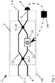
- Fig. 1 shows the quantum optical memristor 1 for manipulating photon quantum states in a first embodiment.
- the quantum optical memristor 1 comprises a Mach-Zehnder interferometer 2 having at a first optical input 3 and a second optical input 4 and having a first optical output 5 and a second optical output 6.
- the first optical input 3 and the first optical output 5 of the Mach-Zehnder interferometer are a first optical input 7 and a first optical output 8 of the quantum optical memristor 1 respectively.
- a detector 9 is configured to detect a time-dependent optical signal n(t) at the second optical output 6 of the Mach-Zehnder interferometer 2.
- a controller 10 configured to compute a target reflectivity R target of the Mach-Zehnder interferometer 2, wherein the controller 10 is configured to update the reflectivity R(t) of the Mach-Zehnder interferometer 2 to match the computed target reflectivity R target .
- the reflectivity of the Mach-Zehnder interferometer is the probability of a photon to change paths 11, 12 in the Mach-Zehnder interferometer 2.
- the controller 10 therefore controls the phase difference of the paths 11, 12, thereby controlling the reflectivity R(t).
- In one of the paths 11, 12 means to change the phase 13 are included, for example a phase retarder, which is controlled by the controller 10.
- the controller 11 is configured to compute the target reflectivity R target based on the derivative of the reflectivity ⁇ (t) with respect to time, wherein the derivative of the reflectivity R(t) with respect to time is a linear function of the detected signal n(t).
- the linear function has an offset proportional to an expected maximum of the signal n(t).
- the maximum of the signal n(t) is 1 or the signal is normalized to 1.
- the photons arrive at distinctive times and cause a sharp signal at the detector.
- the detector also includes a filter, such us a low-pass filter, for example a RC filter. The filter smoothes the signal. Single photons therefore do not cause a single sharp spike in the signal, but rather a signal, which is broad with respect to time.
- the offset guarantees that the derivative of the reflectivity R(t) with respect to time can become negative, although the signal n(t) is restricted to zero and positive values.
- the detector directly measures a signal n meas (t) which is used to estimate the signal n(t) by taking into account the reflectivity R(t) at the respective time.
- a control is implemented in order to prevent the reflectivity R(t) to go to exactly zero, otherwise the feedback could break. This is also reasonable since the reflectivity of a device can never reach exactly zero.
- the estimation only takes into account the signal n(t) within a time frame t-T up to t. This is necessary since a real device cannot measure or store an indefinite signal.
- the behavior of the quantum optical memristor can be tuned by the choice of the length T of the time frame, which is configurable.
- the length T is preferably chosen to be equal to or lower than a modulation or oscillation period T osc of an optical input signal at the optical input 7 of the Mach-Zehnder interferometer 2.
- a low-pass filter for example a RC filter
- the integration time T must be greater than the time constant of the filter.
- two limiting regimes can be accessed.
- the integration time is preferably equal to or smaller than the modulation period.
- the signal n(t) at the detector 9 relates to a detected number of photons.
- the detector is a single-photon detector.
- the Mach-Zehnder interferometer comprises two beam splitters 14, 15, which each have a 50/50 splitting ratio. This splitting ratio is especially beneficial for controlling the reflectivity R(t).
- the quantum optical memristor (1) is partly provided as a part of an integrated photonic chip 16. Namely the Mach-Zehnder interferometer 2 including the beam splitters 14, 15 and means to change the phase 13, such as a retarder, are part of the integrated photonic chip.
- the detector 9 and the controller 10 are external parts.
- the quantum optical memristor 1 can be manufactured in a reliable, stable and reproducible manner. These processes are in addition relatively easy to scale, leading to a low cost per unit. Also, the quantum optical memristor 1 can be realized having small dimensions and being intrinsically compatible with further integrated photonics components.
- the relevant components of the quantum optical memristor 1 are mechanically connected to each other via the integrated photonic chip 16 in a rigid manner. This prevents an undesirable level of phase decoherence of qubits, which could adversely influence the properties of the quantum optical memristor 1.
- thermal phase shifters can be used as means to change the phase 13.
- the quantum optical memristor 1 can be based on glass and is laser-written in the glass.
- the beam splitters 14, 15 are guided directional couplers 17, 18. Guided directional couplers 17,18 are ready and reliable components in integrated photonics and are suited to serve as beam splitters 14, 15 for this application.
- the quantum optical memristor 1 can be used to manipulate photon quantum states by providing the quantum optical memristor 1 with one or more photons at an optical input 7 of the quantum optical memristor 1, measuring an optical signal n(t) at the detector 9 and updating the reflectivity R(t) of the Mach-Zehnder interferometer 2 to match the computed target reflectivity R target .
- the fabrication of the integrated photonic chip can be based on a femtosecond laser micromachining process.
- Single-mode optical waveguides optimised for operation at 1550 nm, are inscribed in an alumino-borosilicate glass (Corning EAGLE XG, 1.1 mm thick) by focusing laser pulses (Yb:KYW cavity-dumped mode-locked laser: 1030 nm wavelength, 300 fs pulse duration, 520 nJ energy per pulse, 1 MHz repetition rate) with a 50 ⁇ objective (0.65 NA) equipped with an aberration-correction collar.
- the entire optical circuit is inscribed at 25 ⁇ m from the bottom surface of the substrate, by translating the substrate at the constant speed of 40 mm/s.
- the inscription process is followed by a thermal annealing composed of a fast rising ramp of 12 °C/min up to 750 °C and by two subsequent slow falling ramps of 12 °C/h and 24 °C/h, respectively down to 630 °C and 500 °C. After that, the cooling process is completed with no control on the temperature ramps.
- the measured insertion loss is 1.2 dB, corresponding to a transmission of 76%.
- S-bend waveguides 40 mm curvature radius
- laser pulses are used (Light Conversion PHAROS: 1030 nm wavelength, 1 ps pulse duration, 1.5 ⁇ J energy per pulse, 20 kHz repetition rate) focused by a 20 ⁇ water-immersion objective (0.50 NA) on the bottom surface of the substrate, while the latter is translated at 4 mm/s entirely immersed in distilled water.
- This fabrication technique is usually referred to as water-assisted laser ablation.
- a metal multilayer film composed of 3 nm of chromium and 100 nm of gold, is deposited on the entire area of the chip by using a magnetron sputtering system.
- a further thermal annealing (rising ramp of 10 °C/min up to 500°C, followed by 60 min at this temperature and by a cooling process with no thermal actuation) is employed to reach a stable value of the electrical resistivity and to prevent electrical drifts that would impair the stability of the phase shifting operation.
- the thermal phase shifters are patterned by laser pulses (Yb:KYW cavity-dumped mode-locked laser: 1030 nm wavelength, 300 fs pulse duration, 200 nJ energy per 669 pulse, 1 MHz repetition rate) focused on the chip surface with a 10 ⁇ objective (0.25 NA).
- laser pulses Yb:KYW cavity-dumped mode-locked laser: 1030 nm wavelength, 300 fs pulse duration, 200 nJ energy per 669 pulse, 1 MHz repetition rate
- contact pads and electrodes are isolated by selectively removing the metal.
- the average electrical resistance of the microheaters is 38 ⁇ , while the resulting electrical power needed to induce a 2n phase shift is as low as 55 mW.
- the photonic chip is mounted on an aluminium heat sink, wire-bonded to a printed circuit board and pigtailed to both input and output single-mode optical fibers. After the pigtailing process, the total insertion loss from input to output fibers is 2 dB, corresponding to a transmission of 63%.
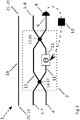
- Figure 2 shows another embodiment of the quantum optical memristor 1.
- the quantum optical memristor comprises a parallel path 19 having an optical input 20 and an optical output 21.
- the optical input 20 and the optical output 21 of the parallel path 19 are a second optical input 22 and a second optical output 2) of the quantum optical memristor 1 respectively.
- the parallel path 19 and the Mach-Zehnder interferometer 2 are configured to be supplied by the same source of photons, in other words the quantum optical memristor 1 is supplied by one source of photons.
- the parallel path 1) essentially does not manipulate the state of the photons in the parallel path 19. No additional components are part of the parallel path 19 which could alter the state of the photons.
- the parallel path 19 is configured to relate to a first spatial mode and the Mach-Zehnder interferometer 2 is configured to relate to a second spatial mode of a qubit encoded as a single photon in a superposition of the first and the second spatial mode.
- the quantum optical memristor 1 is therefore suited to manipulate qubits that are path-encoded rather than being encoded in a superposition of energy states. Path encoded qubits are easier to handle in quantum optics compared to qubits encoded as a superposition of two energy levels.
- the parallel path 19 can be realized as a part of an integrated photonic chip 16 (not shown).
- FIG 3 shows an experimental setup to manipulate single photons including and using the quantum optical memristor 1 according to Figure 2 .
- a collinear Type II SPDC source emits pairs of identical photons at 1550 nm.
- the source is based on a 30 mm PPKTP crystal 24 with a poling period of 46.2 ⁇ m adapted for downconversion from 775 to 1550 nm.
- the crystal is pumped by a CW amplified diode laser 25 (Toptica TA Pro 780) with a pump power of approximately 80 mW.
- the crystal is inserted in a Sagnac interferometer 26 which produces polarization-entagled photons, although in this specific case the entanglement is not used.
- One of the photons is sent directly to the detector 27 for heralding, while the other photon, referred to as the signal, is coupled to the integrated photonic chip 16 via a single-mode fiber 28 which is directly glued to the surface of the photonic chip 16.
- the signal photon goes through the state preparation stage 29, which includes a Mach-Zehnder interferometer 2a with a retarder 13a, and then through the quantum optical memristor 1, which also includes a parallel path 19 so that dual rail or path encoded qubits can be manipulated. Consequently, there is a state tomography stage 35, including a Mach-Zehnder interferometer 2b and a retarder 13b.
- the state tomography stage 35 is used to show that the device preserves some of the initial quantum coherence.
- the controller 10 is pigtailed to single-mode fibers 30 attached to the detectors.
- the output signal goes to an oscilloscope 33b for final data logging, while the feedback signal goes to a controller 10 which computes n (t) and R target and updates the value of the reflectivity R(t) of the quantum optical memristor 1.
- the controller 10 changes the value of the reflectivity R(t) by changing the voltage applied to the thermal phase shifter of the Mach-Zehnder interferometer 2.
- the phase shifter produces a phase shift proportional to the dissipated electrical power.
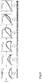
- Fig. 4 shows experimental results (dots) obtained with the experimental setup shown in Fig. 3 and simulations (lines).
- n in is the signal at the input, whereas n out is the output signal.
- the oscillation period T osc is kept constant at 10 s and the integration time T is varied on the range of one oscillation period T osc .
Landscapes
- Physics & Mathematics (AREA)
- General Physics & Mathematics (AREA)
- Engineering & Computer Science (AREA)
- Nonlinear Science (AREA)
- Theoretical Computer Science (AREA)
- Optics & Photonics (AREA)
- Data Mining & Analysis (AREA)
- Condensed Matter Physics & Semiconductors (AREA)
- Computational Mathematics (AREA)
- Evolutionary Computation (AREA)
- Mathematical Analysis (AREA)
- Mathematical Optimization (AREA)
- Pure & Applied Mathematics (AREA)
- Computing Systems (AREA)
- General Engineering & Computer Science (AREA)
- Mathematical Physics (AREA)
- Software Systems (AREA)
- Artificial Intelligence (AREA)
- Optical Modulation, Optical Deflection, Nonlinear Optics, Optical Demodulation, Optical Logic Elements (AREA)
Priority Applications (7)
| Application Number | Priority Date | Filing Date | Title |
|---|---|---|---|
| EP21172766.4A EP4086821A1 (fr) | 2021-05-07 | 2021-05-07 | Memristance optique quantique |
| US18/559,327 US20240241423A1 (en) | 2021-05-07 | 2022-05-06 | Quantum optical memristor |
| JP2023568538A JP7852937B2 (ja) | 2021-05-07 | 2022-05-06 | 量子光学メモリスタ |
| PCT/EP2022/062232 WO2022234058A1 (fr) | 2021-05-07 | 2022-05-06 | Memristance optique quantique |
| CN202280041655.6A CN117480509A (zh) | 2021-05-07 | 2022-05-06 | 量子光学忆阻器 |
| EP22727886.8A EP4334855A1 (fr) | 2021-05-07 | 2022-05-06 | Memristance optique quantique |
| KR1020237041675A KR20240006590A (ko) | 2021-05-07 | 2022-05-06 | 양자 광학 멤리스터 |
Applications Claiming Priority (1)
| Application Number | Priority Date | Filing Date | Title |
|---|---|---|---|
| EP21172766.4A EP4086821A1 (fr) | 2021-05-07 | 2021-05-07 | Memristance optique quantique |
Publications (1)
| Publication Number | Publication Date |
|---|---|
| EP4086821A1 true EP4086821A1 (fr) | 2022-11-09 |
Family
ID=75870487
Family Applications (2)
| Application Number | Title | Priority Date | Filing Date |
|---|---|---|---|
| EP21172766.4A Withdrawn EP4086821A1 (fr) | 2021-05-07 | 2021-05-07 | Memristance optique quantique |
| EP22727886.8A Pending EP4334855A1 (fr) | 2021-05-07 | 2022-05-06 | Memristance optique quantique |
Family Applications After (1)
| Application Number | Title | Priority Date | Filing Date |
|---|---|---|---|
| EP22727886.8A Pending EP4334855A1 (fr) | 2021-05-07 | 2022-05-06 | Memristance optique quantique |
Country Status (6)
| Country | Link |
|---|---|
| US (1) | US20240241423A1 (fr) |
| EP (2) | EP4086821A1 (fr) |
| JP (1) | JP7852937B2 (fr) |
| KR (1) | KR20240006590A (fr) |
| CN (1) | CN117480509A (fr) |
| WO (1) | WO2022234058A1 (fr) |
Cited By (1)
| Publication number | Priority date | Publication date | Assignee | Title |
|---|---|---|---|---|
| GB2625747A (en) * | 2022-12-22 | 2024-07-03 | Universal Quantum Ltd | Improvements in or relating to quantum computing |
Families Citing this family (3)
| Publication number | Priority date | Publication date | Assignee | Title |
|---|---|---|---|---|
| US10858239B2 (en) * | 2018-03-05 | 2020-12-08 | California Institute Of Technology | Techniques for transduction and storage of quantum level signals |
| US12429365B2 (en) * | 2022-10-20 | 2025-09-30 | The Regents Of The University Of Colorado | Quantum sensing and computing using cascaded phases |
| CN117130428B (zh) * | 2022-12-02 | 2024-04-19 | 上海交通大学 | 基于可编程光子芯片的np完全问题实现方法 |
Family Cites Families (13)
| Publication number | Priority date | Publication date | Assignee | Title |
|---|---|---|---|---|
| US5588032A (en) * | 1992-10-14 | 1996-12-24 | Johnson; Steven A. | Apparatus and method for imaging with wavefields using inverse scattering techniques |
| FR2756440B1 (fr) * | 1996-11-28 | 1998-12-31 | Alsthom Cge Alcatel | Dispositif d'emission de donnees optiques |
| GB0103072D0 (en) * | 2001-02-08 | 2001-03-21 | Marconi Comm Ltd | Interferometer |
| CN100454128C (zh) * | 2007-06-15 | 2009-01-21 | 浙江大学 | 实现多光子场波导模式纠缠的系统 |
| CN101350674B (zh) * | 2007-07-16 | 2012-04-04 | 华为技术有限公司 | 一种相位调整的方法、装置及光调制器 |
| WO2010073392A1 (fr) * | 2008-12-26 | 2010-07-01 | 富士通株式会社 | Dispositif de génération de signal optique et son procédé d'ajustement |
| EP2887137B1 (fr) * | 2013-12-19 | 2018-10-10 | Universität Wien | Imagerie quantique avec des photons non détectés |
| EP3446342B1 (fr) * | 2016-04-22 | 2020-03-25 | Oxford University Innovation Limited | Memristance à points quantiques couplés |
| CA3026091A1 (fr) * | 2016-06-02 | 2017-12-07 | Massachusetts Institute Of Technology | Appareil et procedes pour reseau de neurones artificiels optiques |
| WO2018103004A1 (fr) * | 2016-12-07 | 2018-06-14 | 华为技术有限公司 | Procédé de verrouillage de longueur d'onde et laser |
| FR3063352A1 (fr) * | 2017-02-24 | 2018-08-31 | Stmicroelectronics Sa | Modulateur optique en anneau de mach-zender |
| GB201813748D0 (en) * | 2018-08-23 | 2018-10-10 | Univ Hull | Optically switchable memory |
| US11422027B1 (en) * | 2021-02-16 | 2022-08-23 | Hewlett Packard Enterprise Development Lp | Optical switchable system and device |
-
2021
- 2021-05-07 EP EP21172766.4A patent/EP4086821A1/fr not_active Withdrawn
-
2022
- 2022-05-06 KR KR1020237041675A patent/KR20240006590A/ko active Pending
- 2022-05-06 US US18/559,327 patent/US20240241423A1/en active Pending
- 2022-05-06 JP JP2023568538A patent/JP7852937B2/ja active Active
- 2022-05-06 WO PCT/EP2022/062232 patent/WO2022234058A1/fr not_active Ceased
- 2022-05-06 EP EP22727886.8A patent/EP4334855A1/fr active Pending
- 2022-05-06 CN CN202280041655.6A patent/CN117480509A/zh active Pending
Non-Patent Citations (6)
| Title |
|---|
| 0 CHUASUNG MO KANG: "Memristive devices and systems", PROCEEDINGS OF THE IEEE, vol. 64, 1976, pages 209 - 223 |
| MIKEL SANZLUCAS LAMATAENRIQUE SOLANO: "Invited article: Quantum memristors in quantum photonics", APL PHOTONICS, vol. 3, 2018, pages 080801, XP012229409, DOI: 10.1063/1.5036596 |
| PFEIFFER, P.EGUSQUIZA, I. L.DI VENTRA, M.SANZ, M.SOLANO, E.: "Quantum memristors", SCIENTIFIC REPORTS, vol. 6, no. 1, 2016, pages 1 - 6 |
| SALMILEHTO, J.DEPPE, F.DI VENTRA, M.SANZ, M.SOLANO, E: "Quantum memristors with superconducting circuits", SCIENTIFIC REPORTS, vol. 7, no. 1, 2017, pages 1 - 6 |
| SANZ M ET AL: "Invited Article: Quantum memristors in quantum photonics", APL PHOTONICS, AMERICAN INSTITUTE OF PHYSICS, 2 HUNTINGTON QUADRANGLE, MELVILLE, NY 11747, vol. 3, no. 8, 20 June 2018 (2018-06-20), XP012229409, DOI: 10.1063/1.5036596 * |
| TASIO GONZALEZ-RAYA ET AL: "Quantum Memristors in Frequency-Entangled Optical Fields", ARXIV.ORG, CORNELL UNIVERSITY LIBRARY, 201 OLIN LIBRARY CORNELL UNIVERSITY ITHACA, NY 14853, 20 December 2019 (2019-12-20), XP081563511 * |
Cited By (1)
| Publication number | Priority date | Publication date | Assignee | Title |
|---|---|---|---|---|
| GB2625747A (en) * | 2022-12-22 | 2024-07-03 | Universal Quantum Ltd | Improvements in or relating to quantum computing |
Also Published As
| Publication number | Publication date |
|---|---|
| US20240241423A1 (en) | 2024-07-18 |
| CN117480509A (zh) | 2024-01-30 |
| JP7852937B2 (ja) | 2026-04-28 |
| WO2022234058A1 (fr) | 2022-11-10 |
| JP2024522057A (ja) | 2024-06-11 |
| EP4334855A1 (fr) | 2024-03-13 |
| KR20240006590A (ko) | 2024-01-15 |
Similar Documents
| Publication | Publication Date | Title |
|---|---|---|
| US20240241423A1 (en) | Quantum optical memristor | |
| Wang et al. | Continuously tunable ultra-thin silicon waveguide optical delay line | |
| Moreira et al. | Integrated ultra-low-loss 4-bit tunable delay for broadband phased array antenna applications | |
| Lenzini et al. | Active demultiplexing of single photons from a solid‐state source | |
| JP6760976B2 (ja) | チップベースの量子鍵配布 | |
| EP2321696B1 (fr) | Verrou optique intégré | |
| Mondal et al. | Design and analysis of all‐optical 1‐to‐2 line decoder based on linear photonic crystal | |
| Vergyris et al. | On-chip generation of heralded photon-number states | |
| WO2010104956A1 (fr) | Neurone "leaky integrate-and-fire" optique | |
| Ibrahim et al. | Demonstration of a fast-reconfigurable silicon CMOS optical lattice filter | |
| Niels et al. | A high-speed heterogeneous lithium tantalate silicon photonics platform | |
| Geng et al. | Photonic integrated circuit implementation of a sub-GHz-selectivity frequency comb filter for optical clock multiplication | |
| Vázquez et al. | Optical NP problem solver on laser-written waveguide platform | |
| Maeder et al. | On-chip tunable quantum interference in a lithium niobate-on-insulator photonic integrated circuit | |
| Kacmoli et al. | Unidirectional mode selection in bistable quantum cascade ring lasers | |
| Ummethala | Plasmonic-organic and silicon-organic hybrid modulators for high-speed signal processing | |
| Hejda et al. | Optical spike amplitude weighting and neuromimetic rate coding using a joint VCSEL-MRR neuromorphic photonic system | |
| LeGrange et al. | Cascaded all-optical operations in a hybrid integrated 80-Gb/s logic circuit | |
| Ruan et al. | Large phase shifts in As 2 S 3 waveguides for all-optical processing devices | |
| Ke et al. | Tunable optical true time delay line based on ring array | |
| Ni et al. | All-optical phase-controlled phase modulators | |
| Mashanovich et al. | Mid-Infrared Silicon Photonics for Communications | |
| Ren et al. | On-chip Time-bin to Path Qubit Encoding Converter via Thin Film Lithium Niobate Photonics Chip | |
| Saeedi et al. | Differential optical ring modulator: Breaking the bandwidth/quality-factor trade-off | |
| Feng et al. | Non-Hermitian Non-Blocking Switching on a Silicon Integrated Photonic Chip |
Legal Events
| Date | Code | Title | Description |
|---|---|---|---|
| PUAI | Public reference made under article 153(3) epc to a published international application that has entered the european phase |
Free format text: ORIGINAL CODE: 0009012 |
|
| STAA | Information on the status of an ep patent application or granted ep patent |
Free format text: STATUS: THE APPLICATION HAS BEEN PUBLISHED |
|
| AK | Designated contracting states |
Kind code of ref document: A1 Designated state(s): AL AT BE BG CH CY CZ DE DK EE ES FI FR GB GR HR HU IE IS IT LI LT LU LV MC MK MT NL NO PL PT RO RS SE SI SK SM TR |
|
| STAA | Information on the status of an ep patent application or granted ep patent |
Free format text: STATUS: THE APPLICATION IS DEEMED TO BE WITHDRAWN |
|
| 18D | Application deemed to be withdrawn |
Effective date: 20230510 |