EP4086909A1 - Schreiboperationshilfsschaltung - Google Patents
Schreiboperationshilfsschaltung Download PDFInfo
- Publication number
- EP4086909A1 EP4086909A1 EP20910810.9A EP20910810A EP4086909A1 EP 4086909 A1 EP4086909 A1 EP 4086909A1 EP 20910810 A EP20910810 A EP 20910810A EP 4086909 A1 EP4086909 A1 EP 4086909A1
- Authority
- EP
- European Patent Office
- Prior art keywords
- coupled
- input terminal
- inverter
- output terminal
- circuit
- Prior art date
- Legal status (The legal status is an assumption and is not a legal conclusion. Google has not performed a legal analysis and makes no representation as to the accuracy of the status listed.)
- Withdrawn
Links
Images

Classifications
-
- G—PHYSICS
- G11—INFORMATION STORAGE
- G11C—STATIC STORES
- G11C11/00—Digital stores characterised by the use of particular electric or magnetic storage elements; Storage elements therefor
- G11C11/21—Digital stores characterised by the use of particular electric or magnetic storage elements; Storage elements therefor using electric elements
- G11C11/34—Digital stores characterised by the use of particular electric or magnetic storage elements; Storage elements therefor using electric elements using semiconductor devices
- G11C11/40—Digital stores characterised by the use of particular electric or magnetic storage elements; Storage elements therefor using electric elements using semiconductor devices using transistors
- G11C11/401—Digital stores characterised by the use of particular electric or magnetic storage elements; Storage elements therefor using electric elements using semiconductor devices using transistors forming cells needing refreshing or charge regeneration, i.e. dynamic cells
- G11C11/4063—Auxiliary circuits, e.g. for addressing, decoding, driving, writing, sensing or timing
- G11C11/407—Auxiliary circuits, e.g. for addressing, decoding, driving, writing, sensing or timing for memory cells of the field-effect type
- G11C11/409—Read-write [R-W] circuits
- G11C11/4096—Input/output [I/O] data management or control circuits, e.g. reading or writing circuits, I/O drivers or bit-line switches
-
- G—PHYSICS
- G11—INFORMATION STORAGE
- G11C—STATIC STORES
- G11C29/00—Checking stores for correct operation ; Subsequent repair; Testing stores during standby or offline operation
- G11C29/02—Detection or location of defective auxiliary circuits, e.g. defective refresh counters
- G11C29/023—Detection or location of defective auxiliary circuits, e.g. defective refresh counters in clock generator or timing circuitry
-
- G—PHYSICS
- G11—INFORMATION STORAGE
- G11C—STATIC STORES
- G11C11/00—Digital stores characterised by the use of particular electric or magnetic storage elements; Storage elements therefor
- G11C11/21—Digital stores characterised by the use of particular electric or magnetic storage elements; Storage elements therefor using electric elements
- G11C11/34—Digital stores characterised by the use of particular electric or magnetic storage elements; Storage elements therefor using electric elements using semiconductor devices
- G11C11/40—Digital stores characterised by the use of particular electric or magnetic storage elements; Storage elements therefor using electric elements using semiconductor devices using transistors
- G11C11/401—Digital stores characterised by the use of particular electric or magnetic storage elements; Storage elements therefor using electric elements using semiconductor devices using transistors forming cells needing refreshing or charge regeneration, i.e. dynamic cells
- G11C11/4063—Auxiliary circuits, e.g. for addressing, decoding, driving, writing, sensing or timing
- G11C11/407—Auxiliary circuits, e.g. for addressing, decoding, driving, writing, sensing or timing for memory cells of the field-effect type
- G11C11/4076—Timing circuits
-
- G—PHYSICS
- G11—INFORMATION STORAGE
- G11C—STATIC STORES
- G11C11/00—Digital stores characterised by the use of particular electric or magnetic storage elements; Storage elements therefor
- G11C11/21—Digital stores characterised by the use of particular electric or magnetic storage elements; Storage elements therefor using electric elements
- G11C11/34—Digital stores characterised by the use of particular electric or magnetic storage elements; Storage elements therefor using electric elements using semiconductor devices
- G11C11/40—Digital stores characterised by the use of particular electric or magnetic storage elements; Storage elements therefor using electric elements using semiconductor devices using transistors
- G11C11/401—Digital stores characterised by the use of particular electric or magnetic storage elements; Storage elements therefor using electric elements using semiconductor devices using transistors forming cells needing refreshing or charge regeneration, i.e. dynamic cells
- G11C11/4063—Auxiliary circuits, e.g. for addressing, decoding, driving, writing, sensing or timing
- G11C11/407—Auxiliary circuits, e.g. for addressing, decoding, driving, writing, sensing or timing for memory cells of the field-effect type
- G11C11/409—Read-write [R-W] circuits
- G11C11/4094—Bit-line management or control circuits
-
- G—PHYSICS
- G11—INFORMATION STORAGE
- G11C—STATIC STORES
- G11C11/00—Digital stores characterised by the use of particular electric or magnetic storage elements; Storage elements therefor
- G11C11/21—Digital stores characterised by the use of particular electric or magnetic storage elements; Storage elements therefor using electric elements
- G11C11/34—Digital stores characterised by the use of particular electric or magnetic storage elements; Storage elements therefor using electric elements using semiconductor devices
- G11C11/40—Digital stores characterised by the use of particular electric or magnetic storage elements; Storage elements therefor using electric elements using semiconductor devices using transistors
- G11C11/41—Digital stores characterised by the use of particular electric or magnetic storage elements; Storage elements therefor using electric elements using semiconductor devices using transistors forming static cells with positive feedback, i.e. cells not needing refreshing or charge regeneration, e.g. bistable multivibrator or Schmitt trigger
- G11C11/412—Digital stores characterised by the use of particular electric or magnetic storage elements; Storage elements therefor using electric elements using semiconductor devices using transistors forming static cells with positive feedback, i.e. cells not needing refreshing or charge regeneration, e.g. bistable multivibrator or Schmitt trigger using field-effect transistors only
-
- G—PHYSICS
- G11—INFORMATION STORAGE
- G11C—STATIC STORES
- G11C11/00—Digital stores characterised by the use of particular electric or magnetic storage elements; Storage elements therefor
- G11C11/21—Digital stores characterised by the use of particular electric or magnetic storage elements; Storage elements therefor using electric elements
- G11C11/34—Digital stores characterised by the use of particular electric or magnetic storage elements; Storage elements therefor using electric elements using semiconductor devices
- G11C11/40—Digital stores characterised by the use of particular electric or magnetic storage elements; Storage elements therefor using electric elements using semiconductor devices using transistors
- G11C11/41—Digital stores characterised by the use of particular electric or magnetic storage elements; Storage elements therefor using electric elements using semiconductor devices using transistors forming static cells with positive feedback, i.e. cells not needing refreshing or charge regeneration, e.g. bistable multivibrator or Schmitt trigger
- G11C11/413—Auxiliary circuits, e.g. for addressing, decoding, driving, writing, sensing, timing or power reduction
- G11C11/417—Auxiliary circuits, e.g. for addressing, decoding, driving, writing, sensing, timing or power reduction for memory cells of the field-effect type
- G11C11/419—Read-write [R-W] circuits
-
- G—PHYSICS
- G11—INFORMATION STORAGE
- G11C—STATIC STORES
- G11C29/00—Checking stores for correct operation ; Subsequent repair; Testing stores during standby or offline operation
- G11C29/02—Detection or location of defective auxiliary circuits, e.g. defective refresh counters
- G11C29/028—Detection or location of defective auxiliary circuits, e.g. defective refresh counters with adaption or trimming of parameters
-
- G—PHYSICS
- G11—INFORMATION STORAGE
- G11C—STATIC STORES
- G11C7/00—Arrangements for writing information into, or reading information out from, a digital store
- G11C7/10—Input/output [I/O] data interface arrangements, e.g. I/O data control circuits, I/O data buffers
- G11C7/1078—Data input circuits, e.g. write amplifiers, data input buffers, data input registers, data input level conversion circuits
- G11C7/1096—Write circuits, e.g. I/O line write drivers
-
- G—PHYSICS
- G11—INFORMATION STORAGE
- G11C—STATIC STORES
- G11C7/00—Arrangements for writing information into, or reading information out from, a digital store
- G11C7/22—Read-write [R-W] timing or clocking circuits; Read-write [R-W] control signal generators or management
- G11C7/222—Clock generating, synchronizing or distributing circuits within memory device
-
- G—PHYSICS
- G11—INFORMATION STORAGE
- G11C—STATIC STORES
- G11C7/00—Arrangements for writing information into, or reading information out from, a digital store
- G11C7/12—Bit line control circuits, e.g. drivers, boosters, pull-up circuits, pull-down circuits, precharging circuits, equalising circuits, for bit lines
Definitions
- the present disclosure generally relates to Static Random-Access Memory (SRAM) technology field, and more particularly, to a write operation assist circuit.
- SRAM Static Random-Access Memory
- a write operation assist circuit is added to pull down a bit line of the SRAM to a negative voltage, thereby increasing a speed and stability of the write operation.
- Embodiments of the present disclosure provide a write operation assist circuit that does not rely on an external driving signal.
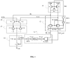
- the drive signal circuit includes a first transmission gate, a second transmission gate, a first inverter and a second inverter
- the first transmission gate has an input terminal coupled to the first bit line, an output terminal coupled to the first input terminal of the programmable delay circuit, a first voltage input terminal coupled to an output terminal of the first inverter, and a second voltage input terminal coupled to an output terminal of the second inverter
- the second transmission gate has an input terminal coupled to the second bit line, an output terminal coupled to the second input terminal of the programmable delay circuit, a first voltage input terminal coupled to the output terminal of the first inverter, and a second voltage input terminal coupled to the output terminal of the second inverter
- the first inverter has an input terminal coupled to the pre-charging signal output terminal of the pre-charging circuit, and the output terminal coupled to an input terminal of the second inverter
- the second inverter has the output terminal coupled to the second voltage input terminal of the first transmission gate and the second voltage input terminal of the second transmission gate.
- the programmable delay circuit includes a NAND gate circuit, a third inverter and a delayer, wherein the NAND gate circuit has a first input terminal serving as the first input terminal of the programmable delay circuit, a second input terminal serving as the second input terminal of the programmable delay circuit, and an output terminal coupled to an input terminal of the third inverter; the third inverter has an output terminal coupled to an input terminal of the delayer; and the delayer has an output terminal serving as the output terminal of the programmable delay circuit, and coupled to the first terminal of the charge pump.
- the write driving circuit includes a sixth inverter and a seventh inverter, wherein the sixth inverter has an input terminal which is input with a first level, and an output terminal serving as the first output terminal of the write driving circuit; the seventh inverter has an input terminal which is input with a second level, and an output terminal serving as the second output terminal of the write driving circuit; and ground terminals of the sixth inverter and the seventh inverter are coupled to the second terminal of the charge pump.
- a write driving circuit outputs a first level to a first bit line, and outputs a second level to a second bit line, and the first level is inverse to the second level.
- a charge pump is driven to operate by the first bit line and the second bit line. Therefore, when writing to a SRAM, no external drive signal is required to drive the charge pump, and no drive signal with strict timing requirements is required.
- the pre-charging circuit 11 has a pre-charging signal output terminal, a first voltage output terminal and a second voltage output terminal.
- the pre-charging signal output terminal may output a pre-charging signal PRE to a pre-charging signal input terminal of the drive signal circuit 12, the first voltage output terminal is coupled to a first bit line BL, and a second voltage output terminal is coupled to a second bit line BLB.
- the pre-charging circuit 11 includes a first PMOS transistor PI, a second PMOS transistor P2 and a third PMOS transistor P3.
- the first transmission gate PG1 is substantially used to transmit a signal on the first bit line BL
- the second transmission gate PG2 is substantially used to transmit a signal on the second bit line BLB.
- the first transmission gate PG1 and the second transmission gate PG2 are turned on or off.
- the first transmission gate PG1 is turned on, the signal on the first bit line BL is input to the first input terminal of the programmable delay circuit 13 via the first transmission gate PG1; when the second transmission gate PG2 is turned on, the signal on the second bit line BLB is input to the second input terminal of the programmable delay circuit 13 via the second transmission gate PG2.
- the delayer Delay 1 has an output terminal serving as the output terminal of the programmable delay circuit 13, and coupled to the first terminal of the charge pump 14.
- the output terminal of the fifth inverter INV5 serves as the output terminal of the programmable delay circuit 13.
- a delay duration of the delayer Delay1 may be adjusted according to actual application requirements. Specifically, the delay duration of the delayer Delay1 may be adjusted according to length of the first bit line BL and the second bit line BLB.
- a full custom memory and memory compiler may be adapted.
- Both a first feedback signal BL_end output by the first transmission gate PG1 and a second feedback signal BL_end output by the second transmission gate PG2 are at a high level, the output terminal of the programmable delay circuit 13 also outputs a high level, the first NMOS transistor M1 is turned on, and VSS_end is pulled down to VSS.
- a waveform of a falling edge of the delay signal Delay generated by the third inverter INV3 is consistent with a waveform of a falling edge of the second bit line BLB.
- the level of the delay signal Delay drops from VDD to VDD/2.
- the waveform of the second bit line BLB is the same as that of the delay signal Delay
- the level of the second bit line BLB is pulled down to VSS at the time point T3 as well.
- the fourth inverter INV4 and the fifth inverter INV5 start to invert, and a Boost signal of a falling edge is obtained, that is, the output signal of the programmable delay circuit 13 is on the falling edge from the time point T3.
- the level of the Boost signal is pulled down from VDD to VSS, and the level of VSS_end is pulled down from VSS to a negative voltage via the capacitor C1.
- the negative voltage of VSS_end is coupled to the NMOS transistors in the sixth inverter INV6 and the seventh inverter INV7.
- Vgs corresponding to an NMOS transistor whose gate is coupled to the negative voltage of VSS_end in the sixth inverter INV6 is higher than 0, the NMOS transistor is turned on, and the level of the second bit line BLB is pulled down to the negative voltage. At this time, the second bit line BLB writes "0" to a memory cell.
- the column selection signal WYS starts a recovery operation
- the level of the column selection signal WYS begins to drop
- the second NMOS transistor M2 and the third NMOS transistor M3 are turned off, and the write driving circuit 15 no longer drives signals input to the bit line BL and the second bit line BLB, and a recovery of the write operation is started.
Landscapes
- Engineering & Computer Science (AREA)
- Microelectronics & Electronic Packaging (AREA)
- Computer Hardware Design (AREA)
- Databases & Information Systems (AREA)
- Static Random-Access Memory (AREA)
- Logic Circuits (AREA)
- Input Circuits Of Receivers And Coupling Of Receivers And Audio Equipment (AREA)
Applications Claiming Priority (2)
| Application Number | Priority Date | Filing Date | Title |
|---|---|---|---|
| CN201911417706.7A CN111179990B (zh) | 2019-12-31 | 2019-12-31 | 写操作辅助电路 |
| PCT/CN2020/130038 WO2021135706A1 (zh) | 2019-12-31 | 2020-11-19 | 写操作辅助电路 |
Publications (2)
| Publication Number | Publication Date |
|---|---|
| EP4086909A1 true EP4086909A1 (de) | 2022-11-09 |
| EP4086909A4 EP4086909A4 (de) | 2023-03-29 |
Family
ID=70646444
Family Applications (1)
| Application Number | Title | Priority Date | Filing Date |
|---|---|---|---|
| EP20910810.9A Withdrawn EP4086909A4 (de) | 2019-12-31 | 2020-11-19 | Schreiboperationshilfsschaltung |
Country Status (5)
| Country | Link |
|---|---|
| US (1) | US12266399B2 (de) |
| EP (1) | EP4086909A4 (de) |
| KR (1) | KR102736260B1 (de) |
| CN (1) | CN111179990B (de) |
| WO (1) | WO2021135706A1 (de) |
Families Citing this family (4)
| Publication number | Priority date | Publication date | Assignee | Title |
|---|---|---|---|---|
| CN111179990B (zh) * | 2019-12-31 | 2021-07-27 | 展讯通信(上海)有限公司 | 写操作辅助电路 |
| US12087355B2 (en) * | 2021-12-17 | 2024-09-10 | Mediatek Inc. | Adaptive control circuit of static random access memory |
| US12260928B2 (en) * | 2022-02-25 | 2025-03-25 | Taiwan Semiconductor Manufacturing Company, Ltd. | Memory devices with backside boost capacitor and methods for forming the same |
| CN120375884B (zh) * | 2025-06-25 | 2026-05-29 | 山东云海国创云计算装备产业创新中心有限公司 | 一种异步存储电路及电子设备 |
Family Cites Families (18)
| Publication number | Priority date | Publication date | Assignee | Title |
|---|---|---|---|---|
| KR100289400B1 (ko) * | 1998-04-30 | 2001-05-02 | 김영환 | 반도체메모리의입출력제어회로 |
| US6351180B1 (en) * | 1999-08-31 | 2002-02-26 | Micron Technology, Inc. | Clamp circuit with fuse options |
| JP4707244B2 (ja) * | 2000-03-30 | 2011-06-22 | ルネサスエレクトロニクス株式会社 | 半導体記憶装置および半導体装置 |
| US6275437B1 (en) * | 2000-06-30 | 2001-08-14 | Samsung Electronics Co., Ltd. | Refresh-type memory with zero write recovery time and no maximum cycle time |
| JP4544808B2 (ja) * | 2002-04-09 | 2010-09-15 | 富士通セミコンダクター株式会社 | 半導体記憶装置の制御方法、および半導体記憶装置 |
| US8120975B2 (en) * | 2009-01-29 | 2012-02-21 | Freescale Semiconductor, Inc. | Memory having negative voltage write assist circuit and method therefor |
| JP5452348B2 (ja) | 2009-07-27 | 2014-03-26 | ルネサスエレクトロニクス株式会社 | 半導体記憶装置 |
| US8687437B2 (en) * | 2010-11-30 | 2014-04-01 | Taiwan Semiconductor Manufacturing Company, Ltd. | Write assist circuitry |
| US8724420B2 (en) * | 2011-05-11 | 2014-05-13 | Taiwan Semiconductor Manufacturing Company, Ltd. | SRAM write assist apparatus |
| WO2013137888A1 (en) * | 2012-03-15 | 2013-09-19 | Intel Corporation | Negative bitline write assist circuit and method for operating the same |
| US9431068B2 (en) * | 2012-10-31 | 2016-08-30 | Mie Fujitsu Semiconductor Limited | Dynamic random access memory (DRAM) with low variation transistor peripheral circuits |
| US8854858B2 (en) * | 2013-01-30 | 2014-10-07 | Texas Instruments Incorporated | Signal level conversion in nonvolatile bitcell array |
| US9070432B2 (en) * | 2013-11-12 | 2015-06-30 | Taiwan Semiconductor Manufacturing Co., Ltd. | Negative bitline boost scheme for SRAM write-assist |
| US9355710B2 (en) | 2014-01-23 | 2016-05-31 | Nvidia Corporation | Hybrid approach to write assist for memory array |
| KR102232922B1 (ko) | 2014-08-11 | 2021-03-29 | 삼성전자주식회사 | 쓰기 보조 회로를 포함하는 스태틱 랜덤 액세스 메모리 장치 |
| US10522214B2 (en) * | 2016-06-09 | 2019-12-31 | Synopsys, Inc. | Robust negative bit-line and reliability aware write assist |
| KR102268704B1 (ko) * | 2017-04-11 | 2021-06-28 | 삼성전자주식회사 | 쓰기 보조 회로를 포함하는 메모리 장치 |
| CN111179990B (zh) * | 2019-12-31 | 2021-07-27 | 展讯通信(上海)有限公司 | 写操作辅助电路 |
-
2019
- 2019-12-31 CN CN201911417706.7A patent/CN111179990B/zh active Active
-
2020
- 2020-11-19 WO PCT/CN2020/130038 patent/WO2021135706A1/zh not_active Ceased
- 2020-11-19 EP EP20910810.9A patent/EP4086909A4/de not_active Withdrawn
- 2020-11-19 KR KR1020227026235A patent/KR102736260B1/ko active Active
- 2020-11-19 US US17/790,281 patent/US12266399B2/en active Active
Also Published As
| Publication number | Publication date |
|---|---|
| CN111179990A (zh) | 2020-05-19 |
| EP4086909A4 (de) | 2023-03-29 |
| CN111179990B (zh) | 2021-07-27 |
| US20220358997A1 (en) | 2022-11-10 |
| WO2021135706A1 (zh) | 2021-07-08 |
| US12266399B2 (en) | 2025-04-01 |
| KR102736260B1 (ko) | 2024-11-29 |
| KR20220125276A (ko) | 2022-09-14 |
Similar Documents
| Publication | Publication Date | Title |
|---|---|---|
| KR102736260B1 (ko) | 기입 조작 보조 회로 | |
| JP6539737B2 (ja) | 走査駆動回路 | |
| WO2020019381A1 (zh) | 一种goa电路、显示面板及显示装置 | |
| WO2020019379A1 (zh) | 一种goa电路、显示面板及显示装置 | |
| WO2020019426A1 (zh) | 包括goa电路的液晶面板及其驱动方法 | |
| KR101639496B1 (ko) | 시프트 레지스터, 게이트 구동 회로, 어레이 기판, 및 디스플레이 디바이스 | |
| CN108428468A (zh) | 移位寄存器及其驱动方法、栅极驱动电路和显示装置 | |
| WO2018218886A1 (zh) | 移位寄存器、栅极驱动电路、显示装置 | |
| CN115050338B (zh) | 栅极驱动电路、显示面板及显示装置 | |
| CN110264940B (zh) | 驱动电路 | |
| US12367804B2 (en) | Gate driving circuit and display panel | |
| US9865334B2 (en) | Efficient bitline driven one-sided power collapse write-assist design for SRAMs | |
| WO2020206816A1 (zh) | Goa 电路及显示面板 | |
| US5952851A (en) | Boosted voltage driver | |
| KR20020002692A (ko) | 고전압 발생 회로 | |
| TWI623926B (zh) | 閘極驅動電路 | |
| JP2018125053A (ja) | 半導体記憶装置および半導体記憶装置の制御方法 | |
| KR100528468B1 (ko) | 반도체 메모리 장치 및 그것의 동작 방법 | |
| US5258956A (en) | High speed sensing device in a semiconductor memory device | |
| TW202030738A (zh) | 移位暫存裝置與顯示裝置 | |
| CN112259033A (zh) | 阵列基板行驱动电路及显示装置 | |
| US9124266B1 (en) | Increasing switching speed of logic circuits | |
| CN111354396B (zh) | 存储器及其写辅助电路 | |
| KR100296322B1 (ko) | 워드라인 부트스트랩 회로 | |
| KR20050029886A (ko) | 반도체 메모리장치의 비트라인 균등화신호 구동회로 |
Legal Events
| Date | Code | Title | Description |
|---|---|---|---|
| STAA | Information on the status of an ep patent application or granted ep patent |
Free format text: STATUS: THE INTERNATIONAL PUBLICATION HAS BEEN MADE |
|
| PUAI | Public reference made under article 153(3) epc to a published international application that has entered the european phase |
Free format text: ORIGINAL CODE: 0009012 |
|
| STAA | Information on the status of an ep patent application or granted ep patent |
Free format text: STATUS: REQUEST FOR EXAMINATION WAS MADE |
|
| 17P | Request for examination filed |
Effective date: 20220721 |
|
| AK | Designated contracting states |
Kind code of ref document: A1 Designated state(s): AL AT BE BG CH CY CZ DE DK EE ES FI FR GB GR HR HU IE IS IT LI LT LU LV MC MK MT NL NO PL PT RO RS SE SI SK SM TR |
|
| A4 | Supplementary search report drawn up and despatched |
Effective date: 20230228 |
|
| RIC1 | Information provided on ipc code assigned before grant |
Ipc: G11C 11/419 20060101AFI20230222BHEP |
|
| DAV | Request for validation of the european patent (deleted) | ||
| DAX | Request for extension of the european patent (deleted) | ||
| GRAP | Despatch of communication of intention to grant a patent |
Free format text: ORIGINAL CODE: EPIDOSNIGR1 |
|
| STAA | Information on the status of an ep patent application or granted ep patent |
Free format text: STATUS: GRANT OF PATENT IS INTENDED |
|
| RIC1 | Information provided on ipc code assigned before grant |
Ipc: G11C 7/12 20060101ALN20241202BHEP Ipc: G11C 29/02 20060101ALI20241202BHEP Ipc: G11C 11/419 20060101AFI20241202BHEP |
|
| RIC1 | Information provided on ipc code assigned before grant |
Ipc: G11C 7/12 20060101ALN20241209BHEP Ipc: G11C 29/02 20060101ALI20241209BHEP Ipc: G11C 11/419 20060101AFI20241209BHEP |
|
| INTG | Intention to grant announced |
Effective date: 20241219 |
|
| STAA | Information on the status of an ep patent application or granted ep patent |
Free format text: STATUS: THE APPLICATION IS DEEMED TO BE WITHDRAWN |
|
| 18D | Application deemed to be withdrawn |
Effective date: 20250423 |