EP4086911B1 - Registre à décalage, circuit d'attaque de grille, et son procédé d'attaque - Google Patents
Registre à décalage, circuit d'attaque de grille, et son procédé d'attaque Download PDFInfo
- Publication number
- EP4086911B1 EP4086911B1 EP20920487.4A EP20920487A EP4086911B1 EP 4086911 B1 EP4086911 B1 EP 4086911B1 EP 20920487 A EP20920487 A EP 20920487A EP 4086911 B1 EP4086911 B1 EP 4086911B1
- Authority
- EP
- European Patent Office
- Prior art keywords
- pull
- transistor
- coupled
- node
- circuit
- Prior art date
- Legal status (The legal status is an assumption and is not a legal conclusion. Google has not performed a legal analysis and makes no representation as to the accuracy of the status listed.)
- Active
Links
Images





Classifications
-
- G—PHYSICS
- G09—EDUCATION; CRYPTOGRAPHY; DISPLAY; ADVERTISING; SEALS
- G09G—ARRANGEMENTS OR CIRCUITS FOR CONTROL OF INDICATING DEVICES USING STATIC MEANS TO PRESENT VARIABLE INFORMATION
- G09G3/00—Control arrangements or circuits, of interest only in connection with visual indicators other than cathode-ray tubes
- G09G3/20—Control arrangements or circuits, of interest only in connection with visual indicators other than cathode-ray tubes for presentation of an assembly of a number of characters, e.g. a page, by composing the assembly by combination of individual elements arranged in a matrix no fixed position being assigned to or needed to be assigned to the individual characters or partial characters
- G09G3/34—Control arrangements or circuits, of interest only in connection with visual indicators other than cathode-ray tubes for presentation of an assembly of a number of characters, e.g. a page, by composing the assembly by combination of individual elements arranged in a matrix no fixed position being assigned to or needed to be assigned to the individual characters or partial characters by control of light from an independent source
- G09G3/36—Control arrangements or circuits, of interest only in connection with visual indicators other than cathode-ray tubes for presentation of an assembly of a number of characters, e.g. a page, by composing the assembly by combination of individual elements arranged in a matrix no fixed position being assigned to or needed to be assigned to the individual characters or partial characters by control of light from an independent source using liquid crystals
- G09G3/3611—Control of matrices with row and column drivers
- G09G3/3674—Details of drivers for scan electrodes
-
- G—PHYSICS
- G09—EDUCATION; CRYPTOGRAPHY; DISPLAY; ADVERTISING; SEALS
- G09G—ARRANGEMENTS OR CIRCUITS FOR CONTROL OF INDICATING DEVICES USING STATIC MEANS TO PRESENT VARIABLE INFORMATION
- G09G3/00—Control arrangements or circuits, of interest only in connection with visual indicators other than cathode-ray tubes
- G09G3/20—Control arrangements or circuits, of interest only in connection with visual indicators other than cathode-ray tubes for presentation of an assembly of a number of characters, e.g. a page, by composing the assembly by combination of individual elements arranged in a matrix no fixed position being assigned to or needed to be assigned to the individual characters or partial characters
- G09G3/34—Control arrangements or circuits, of interest only in connection with visual indicators other than cathode-ray tubes for presentation of an assembly of a number of characters, e.g. a page, by composing the assembly by combination of individual elements arranged in a matrix no fixed position being assigned to or needed to be assigned to the individual characters or partial characters by control of light from an independent source
- G09G3/36—Control arrangements or circuits, of interest only in connection with visual indicators other than cathode-ray tubes for presentation of an assembly of a number of characters, e.g. a page, by composing the assembly by combination of individual elements arranged in a matrix no fixed position being assigned to or needed to be assigned to the individual characters or partial characters by control of light from an independent source using liquid crystals
- G09G3/3611—Control of matrices with row and column drivers
- G09G3/3674—Details of drivers for scan electrodes
- G09G3/3677—Details of drivers for scan electrodes suitable for active matrices only
-
- G—PHYSICS
- G11—INFORMATION STORAGE
- G11C—STATIC STORES
- G11C19/00—Digital stores in which the information is moved stepwise, e.g. shift registers
- G11C19/28—Digital stores in which the information is moved stepwise, e.g. shift registers using semiconductor elements
-
- G—PHYSICS
- G09—EDUCATION; CRYPTOGRAPHY; DISPLAY; ADVERTISING; SEALS
- G09G—ARRANGEMENTS OR CIRCUITS FOR CONTROL OF INDICATING DEVICES USING STATIC MEANS TO PRESENT VARIABLE INFORMATION
- G09G2230/00—Details of flat display driving waveforms
-
- G—PHYSICS
- G09—EDUCATION; CRYPTOGRAPHY; DISPLAY; ADVERTISING; SEALS
- G09G—ARRANGEMENTS OR CIRCUITS FOR CONTROL OF INDICATING DEVICES USING STATIC MEANS TO PRESENT VARIABLE INFORMATION
- G09G2300/00—Aspects of the constitution of display devices
- G09G2300/04—Structural and physical details of display devices
- G09G2300/0404—Matrix technologies
- G09G2300/0408—Integration of the drivers onto the display substrate
-
- G—PHYSICS
- G09—EDUCATION; CRYPTOGRAPHY; DISPLAY; ADVERTISING; SEALS
- G09G—ARRANGEMENTS OR CIRCUITS FOR CONTROL OF INDICATING DEVICES USING STATIC MEANS TO PRESENT VARIABLE INFORMATION
- G09G2300/00—Aspects of the constitution of display devices
- G09G2300/04—Structural and physical details of display devices
- G09G2300/0421—Structural details of the set of electrodes
- G09G2300/0426—Layout of electrodes and connections
-
- G—PHYSICS
- G09—EDUCATION; CRYPTOGRAPHY; DISPLAY; ADVERTISING; SEALS
- G09G—ARRANGEMENTS OR CIRCUITS FOR CONTROL OF INDICATING DEVICES USING STATIC MEANS TO PRESENT VARIABLE INFORMATION
- G09G2310/00—Command of the display device
- G09G2310/02—Addressing, scanning or driving the display screen or processing steps related thereto
- G09G2310/0264—Details of driving circuits
- G09G2310/0267—Details of drivers for scan electrodes, other than drivers for liquid crystal, plasma or OLED displays
-
- G—PHYSICS
- G09—EDUCATION; CRYPTOGRAPHY; DISPLAY; ADVERTISING; SEALS
- G09G—ARRANGEMENTS OR CIRCUITS FOR CONTROL OF INDICATING DEVICES USING STATIC MEANS TO PRESENT VARIABLE INFORMATION
- G09G2310/00—Command of the display device
- G09G2310/02—Addressing, scanning or driving the display screen or processing steps related thereto
- G09G2310/0264—Details of driving circuits
- G09G2310/0286—Details of a shift registers arranged for use in a driving circuit
-
- G—PHYSICS
- G09—EDUCATION; CRYPTOGRAPHY; DISPLAY; ADVERTISING; SEALS
- G09G—ARRANGEMENTS OR CIRCUITS FOR CONTROL OF INDICATING DEVICES USING STATIC MEANS TO PRESENT VARIABLE INFORMATION
- G09G2320/00—Control of display operating conditions
- G09G2320/02—Improving the quality of display appearance
- G09G2320/0257—Reduction of after-image effects
-
- G—PHYSICS
- G09—EDUCATION; CRYPTOGRAPHY; DISPLAY; ADVERTISING; SEALS
- G09G—ARRANGEMENTS OR CIRCUITS FOR CONTROL OF INDICATING DEVICES USING STATIC MEANS TO PRESENT VARIABLE INFORMATION
- G09G3/00—Control arrangements or circuits, of interest only in connection with visual indicators other than cathode-ray tubes
- G09G3/20—Control arrangements or circuits, of interest only in connection with visual indicators other than cathode-ray tubes for presentation of an assembly of a number of characters, e.g. a page, by composing the assembly by combination of individual elements arranged in a matrix no fixed position being assigned to or needed to be assigned to the individual characters or partial characters
- G09G3/22—Control arrangements or circuits, of interest only in connection with visual indicators other than cathode-ray tubes for presentation of an assembly of a number of characters, e.g. a page, by composing the assembly by combination of individual elements arranged in a matrix no fixed position being assigned to or needed to be assigned to the individual characters or partial characters using controlled light sources
- G09G3/30—Control arrangements or circuits, of interest only in connection with visual indicators other than cathode-ray tubes for presentation of an assembly of a number of characters, e.g. a page, by composing the assembly by combination of individual elements arranged in a matrix no fixed position being assigned to or needed to be assigned to the individual characters or partial characters using controlled light sources using electroluminescent panels
- G09G3/32—Control arrangements or circuits, of interest only in connection with visual indicators other than cathode-ray tubes for presentation of an assembly of a number of characters, e.g. a page, by composing the assembly by combination of individual elements arranged in a matrix no fixed position being assigned to or needed to be assigned to the individual characters or partial characters using controlled light sources using electroluminescent panels semiconductive, e.g. using light-emitting diodes [LED]
- G09G3/3208—Control arrangements or circuits, of interest only in connection with visual indicators other than cathode-ray tubes for presentation of an assembly of a number of characters, e.g. a page, by composing the assembly by combination of individual elements arranged in a matrix no fixed position being assigned to or needed to be assigned to the individual characters or partial characters using controlled light sources using electroluminescent panels semiconductive, e.g. using light-emitting diodes [LED] organic, e.g. using organic light-emitting diodes [OLED]
- G09G3/3266—Details of drivers for scan electrodes
-
- G—PHYSICS
- G11—INFORMATION STORAGE
- G11C—STATIC STORES
- G11C19/00—Digital stores in which the information is moved stepwise, e.g. shift registers
- G11C19/28—Digital stores in which the information is moved stepwise, e.g. shift registers using semiconductor elements
- G11C19/287—Organisation of a multiplicity of shift registers
Definitions
- the present disclosure relates to the field of display technologies, and in particular, to a shift register, a gate drive circuit and a drive method thereof.
- a gate drive circuit is used for achieving a shift register function, and each shift register included in the gate drive circuit is coupled to a gate line.
- the gate drive circuit provides output signals (gate scanning signals) for all gate lines row by row, so that the gate lines are driven, and the display apparatus is driven to perform display.
- US 2020/027515 A1 discloses a shift register unit and a method for driving the same, a gate driving circuit, and a display apparatus.
- the shift register unit includes: an input circuit configured to transmit an input signal to a pull-up node; an output circuit configured to transmit a clock signal to an output signal terminal under control of a voltage at the pull-up node; a first reset circuit configured to reset the pull-up node to a first level under control of a first reset signal; a first pull-down control circuit configured to control levels at the pull-up node and the output signal terminal under control of a first control signal; and a first voltage control circuit electrically connected to a second control signal terminal, and configured to control a voltage signal waveform at the first pull-down node under control of a second control signal.
- CN 110767255 A discloses a shift register unit, a driving method, a gate driving circuit, and a display panel.
- the shift register unit includes: first and second signal terminals respectively outputting high and low levels alternately, a level logic of a signal output from the second signal terminal being opposite to that from the first signal terminal; first and second pull-down control circuits; a first pull-down circuit coupled to the first pull-down node, the first signal terminal, and a pull-down target node, and transmitting, in response to a signal of the first pull-down node, the signal of the first signal terminal to the pull-down target node; a second pull-down circuit coupled to the second pull-down node, the second signal terminal, and the pull-down target node, and transmitting, in response to a signal of the second pull-down node, the signal of the second signal terminal to the pull-down target node.
- CN 109559674 A discloses a shift register unit, a method of driving a shift register unit, a gate driving circuit, and a display device are disclosed.
- the shift register unit includes an input circuit and an output circuit.
- the input circuit is connected to the input and the first node.
- the input circuit is configured to write an input signal of the input terminal to the first node in response to an input control signal, so as to control a level of the first node.
- the output circuit is connected to the first node, the clock signal terminal and the pixel signal output terminal.
- the output circuit is configured to receive a clock signal of the clock signal terminal and output a scanning signal through the pixel signal output terminal under control of the level of the first node.
- the output circuit includes a variable resistor, and the variable resistor is configured to adjust a level of the scanning signal according to a resistance value of the variable resistor.
- the present disclosure provides a gate drive circuit which is defined by claim 1.
- the present disclosure provides a drive method of the gate drive circuit which is defined by claim 10.
- first and second are used for descriptive purposes only, and are not to be construed as indicating or implying relative importance or implicitly indicating the number of indicated technical features.
- a feature defined with “first” or “second” may explicitly or implicitly include one or more of the features.
- the term "a plurality of or the plurality of” means two or more unless otherwise specified.
- Coupled and “connected” and their derivatives may be used.
- the term “connected” may be used in the description of some embodiments to indicate that two or more components are in direct physical or electrical contact with each other.
- the term “coupled” may be used in the description of some embodiments to indicate that two or more components are in direct physical or electrical contact.
- the embodiments disclosed herein are not necessarily limited to the contents herein.
- a gate drive circuit includes a plurality of shift registers, and each shift register is electrically connected to a gate line to provide a scanning signal to the gate line electrically connected thereto. Therefore, a plurality of gate lines in the display panel are scanned row by row.
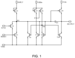
- a shift register includes a plurality of transistors, at least one storage capacitor, a pull-up node PU and a pull-down node PD.
- a level of a first voltage signal transmitted by a first voltage signal terminal VSS1 continues to be a low level
- a level of a second voltage signal transmitted by a second voltage signal terminal VDDo continues to be a high level.
- a drive method of the shift register as shown in FIG. 1 is exemplarily described by considering an example in which the high level is an operation level that enables the transistor to be turned on.
- a transistor T5 and a transistor T6 are turned on to transmit the second voltage signal to the pull-down node PD, so that a potential of the pull-down node PD is raised.
- a transistor T4 is turned on to transmit the first voltage signal received at the first voltage signal terminal VSS1 to the pull-up node PU, so as to perform a noise reduction on the pull-up node PU.
- a level of an input signal transmitted by a signal input terminal INPUT is a high level, and a transistor T1 is turned on to transmit the input signal to the pull-up node PU, so that a voltage of the pull-up node PU is raised.
- a transistor T7 and a transistor T8 are turned on to transmit the first voltage signal received at the first voltage signal terminal VSS1 to the pull-down node PD, so as to pull down the potential of the pull-down node PD and enable the transistor T4 to be turned off.
- the first voltage signal received at the first voltage signal terminal VSS1 is stopped transmitting to the pull-up node PU, which enables the pull-up node PU to be adequately charged.
- a transistor T9 is turned on to transmit a clock signal received at a clock signal terminal CLK to a signal output terminal OUTPUT.
- the potential of the pull-up node PU is firstly raised, so that the transistor T7 and the transistor T8 are turned on under the control of the voltage of the pull-up node PU; and then the potential of the pull-down node PD is pulled down, so that the transistor T4 is controlled to be turned off.
- the first voltage signal is stopped transmitting to the pull-up node PU, which is equivalent to indirectly pulling down the potential of the pull-down node PD.
- the potential of the pull-down node PD may not be pulled down in time due to an existence of a signal delay phenomenon, so that the transistor T4 is still turned on to transmit the first voltage signal to the pull-up node PU.
- the pull-up node PU is unable to be adequately charged, so that the pull-up node PU is insufficiently charged or the voltage of the pull-up node PU is unable to be rapidly raised to an ideal voltage, which affects normal operation of the shift register.
- a pull-down control module composed of the transistor T5, the transistor T6, the transistor T7 and the transistor T8, since the level of the second voltage signal transmitted by the second voltage signal terminal VDDo continues to be the high level, the transistor T5 and the transistor T6 continue to be turned on under control of the second voltage signal.
- the transistor T7 and the transistor T8 are turned on.
- the transistor T5 When the transistor T5, the transistor T6, the transistor T7 and the transistor T8 are all turned on, if the voltage of the pull-down node PD is required to be pulled down to a low voltage, it is necessary to set an appropriate dimension of the transistor (here, the dimension of the transistor refers to a width-to-length ratio of a channel of the transistor). For example, it is necessary to set a dimension of the transistor T7 to be greater than a dimension of the transistor T5, and a dimension of the transistor T8 to be greater than a dimension of the transistor T6, so that the voltage of the pull-down node PD can be pulled down to the low voltage when these four transistors are all turned on. In this way, a manufacturing difficulty will be increased in a manufacturing process of a display substrate.
- the pull-up node PU is unable to be adequately charged, so that the pull-up node PU is insufficiently charged or the voltage of the pull-up node PU is unable to be rapidly raised to an ideal voltage, which affects the normal operation of the shift register.
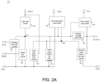
- the shift register RS includes a pull-up node PU, a first pull-down node PDo, a first noise reduction sub-circuit 101, an input sub-circuit 102 and a first pull-down sub-circuit 103.
- the first noise reduction sub-circuit 101 is coupled to the pull-up node PU, the first pull-down node PDo and a first voltage signal terminal VSS1.
- the first noise reduction sub-circuit 101 is configured to transmit a first voltage signal received at the first voltage signal terminal VSS1 to the pull-up node PU under control of a voltage of the first pull-down node PDo.
- the input sub-circuit 102 is coupled to the pull-up node PU and the signal input terminal INPUT.
- the input sub-circuit 102 is configured to transmit an input signal to the pull-up node PU.
- the input sub-circuit 102 is configured to transmit the input signal to the pull-up node PU in response to the input signal received at the signal input terminal INPUT.
- the first pull-down sub-circuit 103 is coupled to the signal input terminal INPUT, the first pull-down node PDo and the first voltage signal terminal VSS1.
- the first pull-down sub-circuit 103 is configured to transmit the first voltage signal received at the first voltage signal terminal VSS1 to the first pull-down node PDo in response to the input signal received at the signal input terminal INPUT, so that the first noise reduction sub-circuit 101 is turned off under control of a voltage of the first voltage signal transmitted to the first pull-down node PDo to stop transmitting the first voltage signal to the pull-up node PU.
- the pull-up node PU does not represent a fixed physical structure, but represents a node having a specific voltage (here, being the voltage of the pull-up node PU), and any point having the specific voltage may be the pull-up node PU.
- the pull-up node PU is not limited to positions shown in the figures. For example, in a case where a resistance of a wire is not considered, any one of points on the wire coupled to the pull-up node PU shown in the figures may be the pull-up node, and a voltage of the points is equal to the voltage of the pull-up node PU.
- the input sub-circuit 102 and the first pull-down sub-circuit 103 are both coupled to the signal input terminal INPUT and are both turned on under control of the input signal transmitted by the signal input terminal INPUT, thereby achieving signal transmission.
- the first pull-down sub-circuit 103 is also turned on under the control of the input signal to transmit the first voltage signal received at the first voltage signal terminal VSS1 to the first pull-down node PDo. As a result, the voltage of the first pull-down node PDo is changed.
- the voltage of the first pull-down node PDo is directly pulled down by the first pull-down sub-circuit 103, so that the first noise reduction sub-circuit 101 is turned off under the control of the voltage of the first voltage signal transmitted to the first pull-down node PDo to stop transmitting the first voltage signal to the pull-up node PU, thereby ensuring the pull-up node PU to be adequately charged.
- the shift register RS provided in the embodiments of the present disclosure adds the first pull-down sub-circuit 103, so that the voltage of the first pull-down node PDo may be rapidly pulled down by the first pull-down sub-circuit 103.
- This manner is more direct and effective, ensures that the pull-up node PU is adequately charged, and avoids that the voltage of the first pull-down node PDo cannot be rapidly pulled down due to a signal delay and the threshold voltage drift of the transistor, which affects the charging of the pull-up node PU. Thus, reliability of a product is improved.
- the first noise reduction sub-circuit 101 includes a first transistor M1.
- a control electrode of the first transistor M1 is coupled to the first pull-down node PDo, a first electrode of the first transistor M1 is coupled to the first voltage signal terminal VSS1, and a second electrode of the first transistor M1 is coupled to the pull-up node PU.
- the first transistor M1 is configured to be turned on under the control of the voltage of the first pull-down node PDo to transmit the first voltage signal received at the first voltage signal terminal VSS1 to the pull-up node PU.
- the input sub-circuit 102 includes a second transistor M2.
- a control electrode of the second transistor M2 is coupled to the signal input terminal INPUT, a first electrode of the second transistor M2 is coupled to the signal input terminal INPUT, and a second electrode of the second transistor M2 is coupled to the pull-up node PU.
- the second transistor M2 is configured to be turned on under control of the input signal to transmit the input signal to the pull-up node PU, so as to charge the pull-up node PU.
- the connection of the second transistor M2 in FIGS. 3A and 3B is for illustration only; and it can be understood from FIGS. 2A and 2B that, the second transistor M2 may also be connected in other way, as long as the second transistor M2 can be turned on to transmit the input signal transmitted by the signal input terminal INPUT to the pull-up node PU.
- the first pull-down sub-circuit 103 includes a third transistor M3.
- a control electrode of the third transistor M3 is coupled to the signal input terminal INPUT, a first electrode of the third transistor M3 is coupled to the first voltage signal terminal VSS1, and a second electrode of the third transistor M3 is coupled to the first pull-down node PDo.
- the third transistor M3 is configured to be turned on under the control of the input signal to transmit the first voltage signal received at the first voltage signal terminal VSS1 to the first pull-down node PDo.
- the shift register in addition to the first noise reduction sub-circuit 101, the input sub-circuit 102 and the first pull-down sub-circuit 103, the shift register also includes other sub-circuits, such as an output sub-circuit, a reset sub-circuit, a pull-down node control sub-circuit, etc.
- the present disclosure does not limit specific arrangement manners of other sub-circuits, as long as the operation of the shift register can be ensured.
- Other sub-circuits included in the shift register RS mentioned below are only a few arrangement manners provided in the present disclosure.
- the shift register RS further includes the first pull-down control sub-circuit 104.
- the first pull-down control sub-circuit 104 is coupled to the first voltage signal terminal VSS1, a second voltage signal terminal VDDo, the pull-up node PU and the first pull-down node PDo.
- the first pull-down control sub-circuit 104 is configured to: transmit a second voltage signal received at the second voltage signal terminal VDDo to the first pull-down node PDo in response to the second voltage signal received at the second voltage signal terminal VDDo and the voltage of the first voltage signal transmitted to the pull-up node PU; and transmit the first voltage signal received at the first voltage signal terminal VSS1 to the first pull-down node PDo in response to the second voltage signal received at the second voltage signal terminal VDDo and a voltage of the input signal transmitted to the pull-up node PU.
- the first pull-down node PDo does not represent a fixed physical structure, but represents a node having a specific voltage (here, being the voltage of the first pull-down node PDo), and any point having the specific voltage may be the first pull-down node PDo.
- the first pull-down node PDo is not limited to positions shown in the figures.
- any one of points on the wire coupled to the first pull-down node PDo shown in the figures may be the first pull-down node, and a voltage of the points is equal to the voltage of the first pull-down node PDo.
- the first pull-down control sub-circuit 104 includes a fourth transistor M4, a fifth transistor M5, a sixth transistor M6, a seventh transistor M7 and a first control node P1.
- a control electrode of the fourth transistor M4 is coupled to the second voltage signal terminal VDDo, a first electrode of the fourth transistor M4 is coupled to the second voltage signal terminal VDDo, and a second electrode of the fourth transistor M4 is coupled to the first control node P1.
- the fourth transistor M4 is configured to be turned on under the control of the second voltage signal to transmit the second voltage signal to the first control node P1.
- a control electrode of the fifth transistor M5 is coupled to the pull-up node PU, a first electrode of the fifth transistor M5 is coupled to the first voltage signal terminal VSS1, and a second electrode of the fifth transistor M5 is coupled to the first control node P1.
- the fifth transistor M5 is configured to be turned on under the control of the voltage of the pull-up node PU to transmit the first voltage signal to the first control node P1.
- a control electrode of the sixth transistor M6 is coupled to the first control node P1, a first electrode of the sixth transistor M6 is coupled to the second voltage signal terminal VDDo, and a second electrode of the sixth transistor M6 is coupled to the first pull-down node PDo.
- the sixth transistor M6 is configured to be turned on under control of a voltage of the first control node P1 to transmit the second voltage signal to the first pull-down node PDo.
- a control electrode of the seventh transistor M7 is coupled to the pull-up node PU, a first electrode of the seventh transistor M7 is coupled to the first voltage signal terminal VSS1, and a second electrode of the seventh transistor M7 is coupled to the first pull-down node PDo.
- the seventh transistor M7 is configured to be turned on under the control of the voltage of the pull-up node PU to transmit the first voltage signal to the first pull-down node PDo.
- the first control node P1 does not represent a fixed physical structure, but represents a node having a specific voltage (here, being the voltage of the first control node P1), and any point having the specific voltage may be the first control node P1.
- the first control node P1 is not limited to positions shown in the figures.
- any one of points on the wire coupled to the first control node P1 shown in the figures may be the first control node, and a voltage of the points is equal to the voltage of the first control node P1.
- the level of the second voltage signal transmitted by the second voltage signal terminal VDDo continues to be the high level
- the high level is the operation level that enables the transistor to be turned on
- the fourth transistor M4 is turned on under the control of the second voltage signal
- the fifth transistor M5 is turned off under the control of the voltage of the pull-up node PU.
- a level of the first control node P1 is the level of the second voltage signal, i.e., the high level.
- the sixth transistor M6 is turned on under the control of the voltage of the first control node P1
- the seventh transistor M7 is turned off under the control of the voltage of the pull-up node PU
- the sixth transistor M6 transmits the second voltage signal received at the second voltage signal terminal VDDo to the first pull-down node PDo, so that the voltage of the first pull-down node PDo is raised.
- the fourth transistor M4 is turned on under the control of the second voltage signal
- the fifth transistor M5 is turned on under the control of the voltage of the pull-up node PU.
- the level of the first control node P1 is the level of the first voltage signal, i.e., the low level.
- the sixth transistor M6 is turned off under the control of the voltage of the first control node P1
- the seventh transistor M7 is turned on under the control of the voltage of the pull-up node PU
- the seventh transistor M7 transmits the first voltage signal received at the first voltage signal terminal VSS1 to the first pull-down node PDo, so that the voltage of the first pull-down node PDo is pulled down.
- the shift register RS further includes: an energy storage sub-circuit 201, a first output sub-circuit 105, a second noise reduction sub-circuit 106 and a reset sub-circuit 107.
- the energy storage sub-circuit 201 is coupled to the pull-up node PU and the first output sub-circuit 105, and the energy storage sub-circuit 201 is configured to store the voltage of the input signal transmitted to the pull-up node PU.
- the first output sub-circuit 105 is further coupled to a clock signal terminal CLK, the pull-up node PU and a first signal output terminal OUTPUT.
- the first output sub-circuit 105 is configured to transmit a clock signal received at the clock signal terminal CLK to the first signal output terminal OUTPUT and the energy storage sub-circuit 201 under the control of the voltage of the input signal transmitted to the pull-up node PU.
- the second noise reduction sub-circuit 106 is coupled to the first pull-down node PDo, a third voltage signal terminal VSS2 and the first signal output terminal OUTPUT.
- the second noise reduction sub-circuit 106 is configured to transmit a third voltage signal received at the third voltage signal terminal VSS2 to the first signal output terminal OUTPUT under the control of the voltage of the first pull-down node PDo, so as to perform the noise reduction processing on the first signal output terminal OUTPUT.
- the reset sub-circuit 107 is coupled to the pull-up node PU, the first voltage signal terminal VSS1 and a reset signal terminal RESET.
- the reset sub-circuit 107 is configured to transmit the first voltage signal received at the first voltage signal terminal VSS1 to the pull-up node PU in response to a reset signal received at the reset signal terminal RESET.
- the first output sub-circuit 105 includes an eighth transistor M8.
- a control electrode of the eighth transistor M8 is coupled to the pull-up node PU, a first electrode of the eighth transistor M8 is coupled to the clock signal terminal CLK, and a second electrode of the eighth transistor M8 is coupled to the first signal output terminal OUTPUT.
- the eighth transistor M8 is configured to transmit the clock signal received at the clock signal terminal CLK to the first signal output terminal OUTPUT under the control of the voltage of the pull-up node PU.
- the energy storage sub-circuit 201 includes a first capacitor. A first terminal of the first capacitor is coupled to the pull-up node PU, and a second terminal of the first capacitor is coupled to the second electrode of the eighth transistor M8.
- the second noise reduction sub-circuit 106 includes a ninth transistor M9.
- a control electrode of the ninth transistor M9 is coupled to the first pull-down node PDo, a first electrode of the ninth transistor M9 is coupled to the third voltage signal terminal VSS2, and a second electrode of the ninth transistor M9 is coupled to the first signal output terminal OUTPUT.
- the ninth transistor M9 is configured to be turned on under the control of the voltage of the first pull-down node PDo to transmit the third voltage signal received at the third voltage signal terminal VSS2 to the first signal output terminal OUTPUT.
- the reset sub-circuit 107 includes a tenth transistor M10.
- a control electrode of the tenth transistor M10 is coupled to the reset signal terminal RESET, a first electrode of the tenth transistor M10 is coupled to the first voltage signal terminal VSS1, and a second electrode of the tenth transistor M10 is coupled to the pull-up node PU.
- the tenth transistor M10 is configured to be turned on under control of the reset signal transmitted by the reset signal terminal RESET to transmit the first voltage signal received at the first voltage signal terminal VSS1 to the pull-up node PU.
- the shift register RS further includes: a second pull-down node PDe, a second pull-down control sub-circuit 108, a third noise reduction sub-circuit 109 and a second pull-down sub-circuit 110.
- the second pull-down control sub-circuit 108 is coupled to the first voltage signal terminal VSS1, a fourth voltage signal terminal VDDe, the pull-up node PU and the second pull-down node PDe.
- the second pull-down control sub-circuit 108 is configured to: transmit a fourth voltage signal received at the fourth voltage signal terminal VDDe to the second pull-down node PDe in response to the fourth voltage signal received at the fourth voltage signal terminal VDDe and the voltage of the first voltage signal transmitted to the pull-up node PU; and transmit the first voltage signal received at the first voltage signal terminal VSS1 to the second pull-down node PDe in response to the fourth voltage signal received at the fourth voltage signal terminal VDDe and the voltage of the input signal transmitted to the pull-up node PU.
- the second pull-down node PDe does not represent a fixed physical structure, but represents a node having a specific voltage (here, being a voltage of the second pull-down node PDe), and any point having the specific voltage may be the second pull-down node PDe.
- the second pull-down node PDe is not limited to positions shown in the figures.
- any one of points on the wire coupled to the second pull-down node PDe shown in the figures may be the second pull-down node, and a voltage of the points is equal to the voltage of the second pull-down node PDe.
- the second pull-down control sub-circuit 108 includes an eleventh transistor M11, a twelfth transistor M12, a thirteenth transistor M13, a fourteenth transistor M14 and a second control node P2.
- a control electrode of the eleventh transistor M11 is coupled to the fourth voltage signal terminal VDDe, a first electrode of the eleventh transistor M11 is coupled to the fourth voltage signal terminal VDDe, and a second electrode of the eleventh transistor M11 is coupled to the second control node P2.
- the eleventh transistor M11 is configured to be turned on under control of the fourth voltage signal transmitted by the fourth voltage signal terminal VDDe to transmit the fourth voltage signal to the second control node P2.
- a control electrode of the twelfth transistor M12 is coupled to the pull-up node PU, a first electrode of the twelfth transistor M12 is coupled to the first voltage signal terminal VSS1, and a second electrode of the twelfth transistor M12 is coupled to the second control node P2.
- the twelfth transistor M12 is turned on under the control of the voltage of the pull-up node PU to transmit the first voltage signal received at the first voltage signal terminal VSS1 to the second control node P2.
- a control electrode of the thirteenth transistor M13 is coupled to the second control node P2, a first electrode of the thirteenth transistor M13 is coupled to the fourth voltage signal terminal VDDe, and a second electrode of the thirteenth transistor M13 is coupled to the second pull-down node PDe.
- the thirteenth transistor M13 is turned on under control of a voltage of the second control node P2 to transmit the fourth voltage signal received at the fourth voltage signal terminal VDDe to the second pull-down node PDe.
- a control electrode of the fourteenth transistor M14 is coupled to the pull-up node PU, a first electrode of the fourteenth transistor M14 is coupled to the first voltage signal terminal VSS1, and a second electrode of the fourteenth transistor M14 is coupled to the second pull-down node PDe.
- the fourteenth transistor M14 is turned on under the control of the voltage of the pull-up node PU to transmit the first voltage signal received at the first voltage signal terminal VSS1 to the second pull-down node PDe.
- the second control node P2 does not represent a fixed physical structure, but represents a node having a specific voltage (here, being a voltage of the second control node P2), and any point having the specific voltage may be the second control node P2.
- the second control node P2 is not limited to positions shown in the figures. For example, in a case where a resistance of a wire is not considered, any one of points on the wire coupled to the second control node P2 shown in the figures may be the second control node, and a voltage of the points is equal to the voltage of the second control node P2.
- a level of the fourth voltage signal transmitted by the fourth voltage signal terminal VDDe continues to be the high level
- the high level is the operation level that enables the transistor to be turned on
- the eleventh transistor M11 is turned on under the control of the fourth voltage signal
- the twelfth transistor M12 is turned off under the control of the voltage of the pull-up node PU.
- a level of the second control node P2 is the level of the fourth voltage signal, e.g., the high level.
- the thirteenth transistor M13 is turned on under the control of the voltage of the second control node P2
- the fourteenth transistor M14 is turned off under the control of the voltage of the pull-up node PU
- the thirteenth transistor M13 transmits the fourth voltage signal received at the fourth voltage signal terminal VDDe to the second pull-down node PDe, so that the voltage of the second pull-down node PDe is raised.
- the eleventh transistor M11 is turned on under the control of the fourth voltage signal
- the twelfth transistor M12 is turned on under the control of the voltage of the pull-up node PU.
- the level of the second control node P2 is the level of the first voltage signal, e.g., the low level.
- the thirteenth transistor M13 is turned off under the control of the voltage of the second control node P2
- the fourteenth transistor M14 is turned on under the control of the voltage of the pull-up node PU
- the fourteenth transistor M14 transmits the first voltage signal received at the first voltage signal terminal VSS1 to the second pull-down node PDe, so that the voltage of the second pull-down node PDe is pulled down.
- the third noise reduction sub-circuit 109 is coupled to the pull-up node PU, the second pull-down node PDe and the first voltage signal terminal VSS1.
- the third noise reduction sub-circuit 109 is configured to transmit the first voltage signal received at the first voltage signal terminal VSS1 to the pull-up node PU under control of a voltage of the fourth voltage signal transmitted to the second pull-down node PDe.
- the second pull-down sub-circuit 110 is coupled to the signal input terminal INPUT, the second pull-down node PDe and the first voltage signal terminal VSS1.
- the second pull-down sub-circuit 110 is configured to transmit the first voltage signal received at the first voltage signal terminal VSS1 to the second pull-down node PDe in response to the input signal received at the signal input terminal INPUT, so that the third noise reduction sub-circuit 109 is turned off under control of the voltage of the first voltage signal transmitted to the second pull-down node PDe to stop transmitting the first voltage signal to the pull-up node PU.
- sub-circuits related to the first pull-down node PDo are the first pull-down control sub-circuit 104, the first pull-down sub-circuit 103, the first noise reduction sub-circuit 101, the second noise reduction sub-circuit 106 (and a fifth noise reduction sub-circuit 113 that will be described later).
- Sub-circuits related to the second pull-down node PDe are the second pull-down control sub-circuit 108, the second pull-down sub-circuit 110, the third noise reduction sub-circuit 109 (and a fourth noise reduction sub-circuit 111 and a sixth noise reduction sub-circuit 114 that will be described later).
- the first pull-down control sub-circuit 104 is used to control a voltage change of the first pull-down node PDo
- the second pull-down control sub-circuit 108 is used to control a voltage change of the second pull-down node PDe.
- the first pull-down sub-circuit 103 and the second pull-down sub-circuit 110 are used to transmit the first voltage signal to the first pull-down node PDo and the second pull-down node PDe, respectively.
- the first noise reduction sub-circuit 101 and the third noise reduction sub-circuit 109 are both used to perform noise reduction on the pull-up node PU
- the second noise reduction sub-circuit 106 and the fourth noise reduction sub-circuit 111 are both used to perform noise reduction on the first signal output terminal OUTPUT
- the fifth noise reduction sub-circuit 113 and the sixth noise reduction sub-circuit 114 are both used to perform noise reduction on a second signal output terminal OC (mentioned later).
- the sub-circuits related to the first pull-down node PDo and the sub-circuits related to the second pull-down node PDe may be regarded as two sets of sub-circuits corresponding to each other.
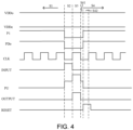
- levels of the second voltage signal transmitted by the second voltage signal terminal VDDo and levels of the fourth voltage signal transmitted by the fourth voltage signal terminal VDDe may be set to alternate between the high level and the low level (for example, as shown in FIG.
- interval time for the levels of the second voltage signal and the levels of the fourth voltage signal to alternate between the high level and the low level is 2s), so that the sub-circuits related to the first pull-down node PDo and the sub-circuits related to the second pull-down node PDe may operate and rest alternately. Therefore, it is possible to avoid a problem of shortening a service life of the sub-circuit caused by continuous operation of the sub-circuit, and prolonging the service life of the sub-circuit.
- the interval time for the levels of the second voltage signal and the levels of the fourth voltage signal to alternate between the high level and the low level may be set according to requirements, and the interval time may be, for example, 1s, 1.5s or the like.
- the third noise reduction sub-circuit 109 includes a fifteenth transistor M15.
- a control electrode of the fifteenth transistor M15 is coupled to the second pull-down node PDe, a first electrode of the fifteenth transistor M15 is coupled to the first voltage signal terminal VSS1, and a second electrode of the fifteenth transistor M15 is coupled to the pull-up node PU.
- the fifteenth transistor M15 is configured to be turned on under the control of the second pull-down node PDe to transmit the first voltage signal received at the first voltage signal terminal VSS1 to the pull-up node PU, so as to perform the noise reduction processing on the pull-up node PU.
- the second pull-down sub-circuit 110 includes a sixteenth transistor M16.
- a control electrode of the sixteenth transistor M16 is coupled to the signal input terminal INPUT, a first electrode of the sixteenth transistor M16 is coupled to the first voltage signal terminal VSS1, and a second electrode of the sixteenth transistor M16 is coupled to the second pull-down node PDe.
- the sixteenth transistor M16 is configured to be turned on under the control of the input signal transmitted by the signal input terminal INPUT to transmit the first voltage signal received at the first voltage signal terminal VSS1 to the second pull-down node PDe.
- the shift register RS further includes the fourth noise reduction sub-circuit 111.
- the fourth noise reduction sub-circuit 111 is coupled to the second pull-down node PDe, the third voltage signal terminal VSS2 and the first signal output terminal OUTPUT.
- the fourth noise reduction sub-circuit 111 is configured to transmit the third voltage signal received at the third voltage signal terminal VSS2 to the first signal output terminal OUTPUT under the control of the voltage of the fourth voltage signal transmitted to the second pull-down node PDe.
- the fourth noise reduction sub-circuit 111 includes a seventeenth transistor M17.
- a control electrode of the seventeenth transistor M17 is coupled to the second pull-down node PDe, a first electrode of the seventeenth transistor M17 is coupled to the third voltage signal terminal VSS2, and a second electrode of the seventeenth transistor M17 is coupled to the first signal output terminal OUTPUT.
- the seventeenth transistor M17 is configured to be turned on under the control of the second pull-down node PDe to transmit the third voltage signal received at the third voltage signal terminal VSS2 to the first signal output terminal OUTPUT.
- the shift register RS further includes: a second output sub-circuit 112, the fifth noise reduction sub-circuit 113 and the sixth noise reduction sub-circuit 114.
- the second output sub-circuit 112 is coupled to the pull-up node PU, the clock signal terminal CLK and the second signal output terminal OC.
- the second output sub-circuit 112 is configured to transmit the clock signal received at the clock signal terminal CLK to the second signal output terminal OC under the control of the voltage of the input signal transmitted to the pull-up node PU.
- the fifth noise reduction sub-circuit 113 is coupled to the first pull-down node PDo, the first voltage signal terminal VSS1 and the second signal output terminal OC.
- the fifth noise reduction sub-circuit 113 is configured to transmit the first voltage signal received at the first voltage signal terminal VSS1 to the second signal output terminal OC under the control of the voltage of the second voltage signal transmitted to the first pull-down node PDo.
- the sixth noise reduction sub-circuit 114 is coupled to the second pull-down node PDe, the first voltage signal terminal VSS1 and the second signal output terminal OC.
- the sixth noise reduction sub-circuit 114 is configured to transmit the first voltage signal received at the first voltage signal terminal VSS1 to the second signal output terminal OC under the control of the voltage of the fourth voltage signal transmitted to the second pull-down node PDe.
- the shift register RS provided in some embodiments of the present disclosure includes the first output sub-circuit 105 and the second output sub-circuit 112, and the first output sub-circuit 105 and the second output sub-circuit 112 output the clock signal to the first signal output terminal OUTPUT and the second signal output terminal OC, respectively.
- the gate drive circuit includes a plurality of shift registers RS, and adjacent shift registers RS need to be cascaded; thus, one of the first signal output terminal OUTPUT and the second signal output terminal OC may be coupled to the gate line to serve as a port for outputting a gate scanning signal to a display area of the display panel (for example, the first signal output terminal OUTPUT is coupled to the gate line), and the other of the first signal output terminal OUTPUT and the second signal output terminal OC serves as a port for coupling when the adjacent shift registers RS are cascaded.
- a signal input terminal INPUT of an any-stage shift register RS except a first-stage shift register RS is coupled to a second signal output terminal OC of a previous-stage shift register RS of the any-stage shift register RS.
- the second output sub-circuit 112 includes an eighteenth transistor M18.
- a control electrode of the eighteenth transistor M18 is coupled to the pull-up node PU, a first electrode of the eighteenth transistor M18 is coupled to the clock signal terminal CLK, and a second electrode of the eighteenth transistor M18 is coupled to the second signal output terminal OC.
- the eighteenth transistor M18 is configured to be turned on under the control of the voltage of the pull-up node PU to transmit the clock signal received at the clock signal terminal CLK to the second signal output terminal OC.
- the fifth noise reduction sub-circuit 113 includes a nineteenth transistor M19.
- a control electrode of the nineteenth transistor M19 is coupled to the first pull-down node PDo, a first electrode of the nineteenth transistor M19 is coupled to the first voltage signal terminal VSS1, and a second electrode of the nineteenth transistor M19 is coupled to the second signal output terminal OC.
- the nineteenth transistor M19 is configured to be turned on under the control of the first pull-down node PDo to transmit the first voltage signal received at the first voltage signal terminal VSS1 to the second signal output terminal OC.
- the sixth noise reduction sub-circuit 114 includes a twentieth transistor M20.
- a control electrode of the twentieth transistor M20 is coupled to the second pull-down node PDe, a first electrode of the twentieth transistor M20 is coupled to the first voltage signal terminal VSS1, and a second electrode of the twentieth transistor M20 is coupled to the second signal output terminal OC.
- the twentieth transistor M20 is configured to be turned on under the control of the second pull-down node PDe to transmit the first voltage signal received at the first voltage signal terminal VSS1 to the second signal output terminal OC.
- the shift register RS further includes an initialization sub-circuit 115.
- the initialization sub-circuit 115 is coupled to the pull-up node PU, an initialization signal terminal STV0 and the first voltage signal terminal VSS1.
- the initialization sub-circuit 115 is configured to transmit the first voltage signal received at the first voltage signal terminal VSS1 to the pull-up node PU in response to an initialization signal received at the initialization signal terminal STV0.
- the initialization sub-circuit 115 includes a twenty-first transistor M21.
- a control electrode of the twenty-first transistor M21 is coupled to the initialization signal terminal STVO, a first electrode of the twenty-first transistor M21 is coupled to the first voltage signal terminal VSS1, and a second electrode of the twenty-first transistor M21 is coupled to the pull-up node PU.
- the twenty-first transistor M21 is configured to be turned on under control of the initialization signal transmitted by the initialization signal terminal STV0 to transmit the first voltage signal received at the first voltage signal terminal VSS1 to the pull-up node PU.
- the shift register RS includes: the pull-up node PU, the first pull-down node PDo, the second pull-down node PDe, the first noise reduction sub-circuit 101, the input sub-circuit 102, the first pull-down sub-circuit 103, the first pull-down control sub-circuit 104, the first output sub-circuit 105, the energy storage sub-circuit 201, the second noise reduction sub-circuit 106, the reset sub-circuit 107, the second pull-down control sub-circuit 108, the third noise reduction sub-circuit 109, the second pull-down sub-circuit 110, the fourth noise reduction sub-circuit 111, the second output sub-circuit 112, the fifth noise reduction sub-circuit 113, the sixth noise reduction sub-circuit 114 and the initialization sub-circuit 115.
- the first noise reduction sub-circuit 101 includes the first transistor M1, the input sub-circuit 102 includes the second transistor M2, the first pull-down sub-circuit 103 includes the third transistor M3, and the first pull-down control sub-circuit 104 includes the fourth transistor M4, the fifth transistor M5, the sixth transistor M6, the seventh transistor M7 and the first control node P1.
- the first output sub-circuit 105 includes the eighth transistor M8, the energy storage sub-circuit 201 includes the first capacitor, the second noise reduction sub-circuit 106 includes the ninth transistor M9, and the reset sub-circuit 107 includes the tenth transistor M10.
- the second pull-down control sub-circuit 108 includes the eleventh transistor M11, the twelfth transistor M12, the thirteenth transistor M13, the fourteenth transistor M14 and the second control node P2; the third noise reduction sub-circuit 109 includes the fifteenth transistor M15; the second pull-down sub-circuit 110 includes the sixteenth transistor M16; and the fourth noise reduction sub-circuit 111 includes the seventeenth transistor M17.
- the second output sub-circuit 112 includes the eighteenth transistor M18, the fifth noise reduction sub-circuit 113 includes the nineteenth transistor M19, the sixth noise reduction sub-circuit 114 includes the twentieth transistor M20, and the initialization sub-circuit 115 includes the twenty-first transistor M21.
- the control electrode of the first transistor M1 is coupled to the first pull-down node PDo, the first electrode of the first transistor M1 is coupled to the first voltage signal terminal VSS1, and the second electrode of the first transistor M1 is coupled to the pull-up node PU.
- the first transistor M1 is configured to be turned on under the control of the voltage of the first pull-down node PDo to transmit the first voltage signal received at the first voltage signal terminal VSS1 to the pull-up node PU.
- the control electrode of the second transistor M2 is coupled to the signal input terminal INPUT, the first electrode of the second transistor M2 is coupled to the signal input terminal INPUT, and the second electrode of the second transistor M2 is coupled to the pull-up node PU.
- the second transistor M2 is configured to be turned on under the control of the input signal to transmit the input signal to the pull-up node PU, so as to charge the pull-up node PU.
- the control electrode of the third transistor M3 is coupled to the signal input terminal INPUT, the first electrode of the third transistor M3 is coupled to the first voltage signal terminal VSS1, and the second electrode of the third transistor M3 is coupled to the first pull-down node PDo.
- the third transistor M3 is configured to be turned on under the control of the input signal to transmit the first voltage signal received at the first voltage signal terminal VSS1 to the first pull-down node PDo.
- the control electrode of the fourth transistor M4 is coupled to the second voltage signal terminal VDDo, the first electrode of the fourth transistor M4 is coupled to the second voltage signal terminal VDDo, and the second electrode of the fourth transistor M4 is coupled to the first control node P1.
- the fourth transistor M4 is configured to be turned on under the control of the second voltage signal to transmit the second voltage signal to the first control node P1.
- the control electrode of the fifth transistor M5 is coupled to the pull-up node PU, the first electrode of the fifth transistor M5 is coupled to the first voltage signal terminal VSS1, and the second electrode of the fifth transistor M5 is coupled to the first control node P1.
- the fifth transistor M5 is configured to be turned on under the control of the voltage of the pull-up node PU to transmit the first voltage signal to the first control node P1.
- the control electrode of the sixth transistor M6 is coupled to the first control node P1, the first electrode of the sixth transistor M6 is coupled to the second voltage signal terminal VDDo, and the second electrode of the sixth transistor M6 is coupled to the first pull-down node PDo.
- the sixth transistor M6 is configured to be turned on under the control of the voltage of the first control node P1 to transmit the second voltage signal to the first pull-down node PDo.
- the control electrode of the seventh transistor M7 is coupled to the pull-up node PU, the first electrode of the seventh transistor M7 is coupled to the first voltage signal terminal VSS1, and the second electrode of the seventh transistor M7 is coupled to the first pull-down node PDo.
- the seventh transistor M7 is configured to be turned on under the control of the voltage of the pull-up node PU to transmit the first voltage signal to the first pull-down node PDo.
- the control electrode of the eighth transistor M8 is coupled to the pull-up node PU, the first electrode of the eighth transistor M8 is coupled to the clock signal terminal CLK, and the second electrode of the eighth transistor M8 is coupled to the first signal output terminal OUTPUT.
- the eighth transistor M8 is configured to transmit the clock signal received at the clock signal terminal CLK to the first signal output terminal OUTPUT under the control of the voltage of the pull-up node PU.
- the first terminal of the first capacitor is coupled to the pull-up node PU, and the second terminal of the first capacitor is coupled to the second electrode of the eighth transistor M8.
- the control electrode of the ninth transistor M9 is coupled to the first pull-down node PDo, the first electrode of the ninth transistor M9 is coupled to the third voltage signal terminal VSS2, and the second electrode of the ninth transistor M9 is coupled to the first signal output terminal OUTPUT.
- the ninth transistor M9 is configured to be turned on under the control of the voltage of the first pull-down node PDo to transmit the third voltage signal received at the third voltage signal terminal VSS2 to the first signal output terminal OUTPUT.
- the control electrode of the tenth transistor M10 is coupled to the reset signal terminal RESET, the first electrode of the tenth transistor M10 is coupled to the first voltage signal terminal VSS1, and the second electrode of the tenth transistor M10 is coupled to the pull-up node PU.
- the tenth transistor M10 is configured to be turned on under the control of the reset signal transmitted by the reset signal terminal RESET to transmit the first voltage signal received at the first voltage signal terminal VSS1 to the pull-up node PU.
- the control electrode of the eleventh transistor M11 is coupled to the fourth voltage signal terminal VDDe, the first electrode of the eleventh transistor M11 is coupled to the fourth voltage signal terminal VDDe, and the second electrode of the eleventh transistor M11 is coupled to the second control node P2.
- the eleventh transistor M11 is configured to be turned on under the control of the fourth voltage signal transmitted by the fourth voltage signal terminal VDDe to transmit the fourth voltage signal to the second control node P2.
- the control electrode of the twelfth transistor M12 is coupled to the pull-up node PU, the first electrode of the twelfth transistor M12 is coupled to the first voltage signal terminal VSS1, and the second electrode of the twelfth transistor M12 is coupled to the second control node P2.
- the twelfth transistor M12 is turned on under the control of the voltage of the pull-up node PU to transmit the first voltage signal received at the first voltage signal terminal VSS1 to the second control node P2.
- the control electrode of the thirteenth transistor M13 is coupled to the second control node P2, the first electrode of the thirteenth transistor M13 is coupled to the fourth voltage signal terminal VDDe, and the second electrode of the thirteenth transistor M13 is coupled to the second pull-down node PDe.
- the thirteenth transistor M13 is turned on under the control of the voltage of the second control node P2 to transmit the fourth voltage signal received at the fourth voltage signal terminal VDDe to the second pull-down node PDe.
- the control electrode of the fourteenth transistor M14 is coupled to the pull-up node PU, the first electrode of the fourteenth transistor M14 is coupled to the first voltage signal terminal VSS1, and the second electrode of the fourteenth transistor M14 is coupled to the second pull-down node PDe.
- the fourteenth transistor M14 is turned on under the control of the voltage of the pull-up node PU to transmit the first voltage signal received at the first voltage signal terminal VSS1 to the second pull-down node PDe.
- the control electrode of the fifteenth transistor M15 is coupled to the second pull-down node PDe, the first electrode of the fifteenth transistor M15 is coupled to the first voltage signal terminal VSS1, and the second electrode of the fifteenth transistor M15 is coupled to the pull-up node PU.
- the fifteenth transistor M15 is configured to be turned on under the control of the second pull-down node PDe to transmit the first voltage signal received at the first voltage signal terminal VSS1 to the pull-up node PU, so as to perform the noise reduction processing on the pull-up node PU.
- the control electrode of the sixteenth transistor M16 is coupled to the signal input terminal INPUT, the first electrode of the sixteenth transistor M16 is coupled to the first voltage signal terminal VSS1, and the second electrode of the sixteenth transistor M16 is coupled to the second pull-down node PDe.
- the sixteenth transistor M16 is configured to be turned on under the control of the input signal transmitted by the signal input terminal INPUT to transmit the first voltage signal received at the first voltage signal terminal VSS1 to the second pull-down node PDe.
- the control electrode of the seventeenth transistor M17 is coupled to the second pull-down node PDe, the first electrode of the seventeenth transistor M17 is coupled to the third voltage signal terminal VSS2, and the second electrode of the seventeenth transistor M17 is coupled to the first signal output terminal OUTPUT.
- the seventeenth transistor M17 is configured to be turned on under the control of the second pull-down node PDe to transmit the third voltage signal received at the third voltage signal terminal VSS2 to the first signal output terminal OUTPUT.
- the control electrode of the eighteenth transistor M18 is coupled to the pull-up node PU, the first electrode of the eighteenth transistor M18 is coupled to the clock signal terminal CLK, and the second electrode of the eighteenth transistor M18 is coupled to the second signal output terminal OC.
- the eighteenth transistor M18 is configured to be turned on under the control of the voltage of the pull-up node PU to transmit the clock signal received at the clock signal terminal CLK to the second signal output terminal OC.
- the control electrode of the nineteenth transistor M19 is coupled to the first pull-down node PDo, the first electrode of the nineteenth transistor M19 is coupled to the first voltage signal terminal VSS1, and the second electrode of the nineteenth transistor M19 is coupled to the second signal output terminal OC.
- the nineteenth transistor M19 is configured to be turned on under the control of the first pull-down node PDo to transmit the first voltage signal received at the first voltage signal terminal VSS1 to the second signal output terminal OC.
- the control electrode of the twentieth transistor M20 is coupled to the second pull-down node PDe, the first electrode of the twentieth transistor M20 is coupled to the first voltage signal terminal VSS1, and the second electrode of the twentieth transistor M20 is coupled to the second signal output terminal OC.
- the twentieth transistor M20 is configured to be turned on under the control of the second pull-down node PDe to transmit the first voltage signal received at the first voltage signal terminal VSS1 to the second signal output terminal OC.
- the control electrode of the twenty-first transistor M21 is coupled to the initialization signal terminal STVO, the first electrode of the twenty-first transistor M21 is coupled to the first voltage signal terminal VSS1, and the second electrode of the twenty-first transistor M21 is coupled to the pull-up node PU.
- the twenty-first transistor M21 is configured to be turned on under the control of the initialization signal transmitted by the initialization signal terminal STV0 to transmit the first voltage signal received at the first voltage signal terminal VSS1 to the pull-up node PU.
- the transistor used in the shift register RS provided in the embodiments of the present disclosure may be an N-type transistor or a P-type transistor.
- the transistors in the shift register RS provided in the embodiments of the present disclosure are all N-type transistors.
- the transistor used in the shift register RS provided in the embodiments of the present disclosure may be an enhancement-type transistor, a depletion-type transistor or any other switching device with the same property.
- the transistor may also be an amorphous silicon thin film transistor, a polycrystalline silicon thin film transistor or an amorphous indium gallium zinc oxide thin film transistor, and the present disclosure is not limited thereto.
- the control electrode of the transistor in the shift register RS is a gate of the transistor
- the first electrode of the transistor may be a source
- the second electrode of the transistor may be a drain
- the first electrode of the transistor may be the drain
- the second electrode of the transistor may be the source
- the present disclosure is not limited thereto.
- the source and the drain of the transistor may be symmetrical in structure
- the source and the drain thereof may be indistinguishable in structure. That is, the first electrode and the second electrode of the transistor in the embodiments of the present disclosure may be indistinguishable in structure.
- the transistor is the P-type transistor
- the first electrode of the transistor is the source
- the second electrode of the transistor is the drain.
- the first electrode of the transistor is the drain
- the second electrode of the transistor is the source.
- high voltage and low voltage are relative.
- the transistor included in the shift register is the N-type transistor
- a voltage that enables the transistor to be turned on is referred to as the high voltage (the high potential, or the high level)
- the low voltage the low potential, or the low level
- the transistor included in the shift register is the P-type transistor
- a voltage that is unable to make the transistor be turned on is referred to as the high voltage (the high potential, or the high level)
- a voltage that enables the transistor to be turned on is referred to as the low voltage (the low potential, or the low level).
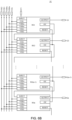
- the gate drive circuit 01 includes at least two cascaded shift registers RS as provided in the above embodiments of the present disclosure.
- the gate drive circuit 01 includes n cascaded shift registers RS as described above, which are RS1 to RSn.
- a signal input terminal INPUT of the first-stage shift register RS1 is coupled to a start signal terminal STV.
- the signal input terminal INPUT of the any-stage shift register RS except the first-stage shift register RS1 is coupled to a first signal output terminal OUTPUT of the previous-stage shift register RS of the any-stage shift register RS.
- a signal input terminal INPUT of a second-stage shift register RS2 is coupled to a first signal output terminal OUTPUT of the first-stage shift register RS1.
- a signal input terminal INPUT of a third-stage shift register RS3 is coupled to a first signal output terminal OUTPUT of the second-stage shift register RS2.
- a reset signal terminal RESET of the any-stage shift register RS except a last-stage shift register RSn is coupled to a first signal output terminal OUTPUT of a next-stage shift register RS of the any-stage shift register RS.
- a reset signal terminal RESET of the second-stage shift register RS2 is coupled to a first signal output terminal OUTPUT of the third-stage shift register RS3.
- a reset signal terminal RESET of the third-stage shift register RS3 is coupled to a first signal output terminal OUTPUT of a fourth-stage shift register RS4.
- a reset signal terminal RESET of the last-stage shift register RSn is coupled to a signal terminal separately provided for outputting the reset signal, or is coupled to the start signal terminal STV.
- FIG. 6A is only schematically illustrated by considering an example in which the reset signal terminal RESET of the last-stage shift register RSn is coupled to the signal terminal separately provided for outputting the reset signal).
- the signal input terminal INPUT of the first-stage shift register RS1 is coupled to the start signal terminal STV.
- the signal input terminal INPUT of the any-stage shift register RS except the first-stage shift register RS1 is coupled to a second signal output terminal OC of the previous-stage shift register RS of the any-stage shift register RS.
- the signal input terminal INPUT of the second-stage shift register RS2 is coupled to a second signal output terminal OC of the first-stage shift register RS1.
- the signal input terminal INPUT of the third-stage shift register RS3 is coupled to a second signal output terminal OC of the second-stage shift register RS2.
- the reset signal terminal RESET of the any-stage shift register RS except the last-stage shift register RSn is coupled to a second signal output terminal OC of the next-stage shift register RS of the any-stage shift register RS.
- the reset signal terminal RESET of the second-stage shift register RS2 is coupled to a second signal output terminal OC of the third-stage shift register RS3.
- the reset signal terminal RESET of the third-stage shift register RS3 is coupled to a second signal output terminal OC of the fourth-stage shift register RS4.
- the reset signal terminal RESET of the last-stage shift register RSn is coupled to a signal terminal separately provided for outputting the reset signal, or is coupled to the start signal terminal STV.
- FIG. 6B is only schematically illustrated by considering an example in which the reset signal terminal RESET of the last-stage shift register RSn is coupled to the signal terminal separately provided for outputting the reset signal).
- the first signal output terminal OUTPUT of each shift register RS is coupled to a single gate line.
- the first signal output terminal OUTPUT is configured to output the gate scanning signal to the gate line to drive the gate line.
- each shift register RS may be coupled to a single gate line
- the first signal output terminal OUTPUT serves as the port for cascading the adjacent shift register RS, and the present disclosure is not limited thereto.
- the gate drive circuit 01 provided in the embodiments of the present disclosure includes the shift register RS as described above, it has the same beneficial effects as the shift register RS provided in the foregoing embodiments.
- the foregoing embodiments have described the structure and the beneficial effects of the shift register RS in detail, which will not be repeated here.
- one of the first signal output terminal OUTPUT and the second signal output terminal OC of the shift register RS is coupled to the gate line to serve as the port for outputting the gate scanning signal to the display area of the display panel, and the other of the first signal output terminal OUTPUT and the second signal output terminal OC serves as the port for coupling when the adjacent shift registers RS are cascaded.
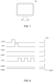
- some embodiments of the present disclosure further provide a display apparatus 100.
- the display apparatus 100 includes the above gate drive circuit 01 provided in the present disclosure, i.e., includes the above shift register RS.
- the display apparatus 100 has the same beneficial effects as the shift register RS provided in the foregoing embodiments.
- the foregoing embodiments have described the structure and the beneficial effects of the shift register RS in detail, which will not be repeated here.
- the display apparatus 100 provided in the embodiments of the present disclosure is a liquid crystal display apparatus; or the display apparatus 100 provided in the embodiments of the present disclosure is an organic light-emitting diode display apparatus including an organic light-emitting diode display panel.
- the display apparatus provided in the embodiments of the present disclosure may be any product or component having a display function, such as a liquid crystal panel, an electronic paper, an organic light-emitting diode (OLED) panel, a mobile phone, a tablet computer, a television, a display, a notebook computer, a digital photo frame, a navigator or the like, and the present disclosure is not limited thereto.
- Some embodiments of the present disclosure further provide a drive method of the gate drive circuit, and the drive method is applied to the gate drive circuit as described above.
- the drive method includes a noise reduction phase S1 and a charging phase S2 included in a frame period for each shift register RS in the gate drive circuit 01.
- the noise reduction phase S1 includes: the first noise reduction sub-circuit 101 transmitting the first voltage signal received at the first voltage signal terminal VSS1 to the pull-up node PU after the first noise reduction sub-circuit 101 is turned on under the control of the voltage of the first pull-down node PDo.
- the noise reduction phase S1 includes: the first transistor M1 transmitting the first voltage signal received at the first voltage signal terminal VSS1 to the pull-up node PU after the first transistor M1 is turned on under the control of the voltage of the first pull-down node PDo, so as to perform the noise reduction processing on the pull-up node PU.
- the charging phase S2 includes:
- the charging phase S2 includes following steps.
- the second transistor M2 transmits the input signal received at the signal input terminal INPUT to the pull-up node PU after the second transistor M2 is turned on under the control of the input signal; the third transistor M3 transmits the first voltage signal received at the first voltage signal terminal VSS1 to the first pull-down node PDo after the third transistor M3 is turned on under the control of the input signal; and the first transistor M1 stops transmitting the first voltage signal received at the first voltage signal terminal VSS1 to the pull-up node PU after the first transistor M1 is turned off under the control of the voltage of the first pull-down node PDo.
- the first pull-down sub-circuit 103 is also turned on under the control of the input signal to transmit the first voltage signal received at the first voltage signal terminal VSS1 to the first pull-down node PDo, so that the voltage of the first pull-down node PDo changes, and the first noise reduction sub-circuit 101 is turned off under the control of the voltage of the first pull-down node PDo to stop transmitting the first voltage signal to the pull-up node PU. Therefore, it is ensured that the pull-up node PU may be adequately charged.
- the voltage of the first pull-down node PDo may be rapidly pulled down by the first pull-down sub-circuit 103. This manner is more direct and effective, ensures that the pull-up node PU is adequately charged, and avoids that the voltage of the first pull-down node PDo cannot be rapidly pulled down due to the signal delay and the threshold voltage drift of the transistor, which affects the charging of the pull-up node PU. Thus, the reliability of the product is improved.
- the drive method of the gate drive circuit includes the noise reduction phase S1, the charging phase S2, an output phase S3 and a reset phase S4.
- the noise reduction phase S1 further includes a following step.
- the second noise reduction sub-circuit 106 transmits the third voltage signal received at the third voltage signal terminal VSS2 to the first signal output terminal OUTPUT after the second noise reduction sub-circuit 106 is turned on under the control of the voltage of the first pull-down node PDo.
- the noise reduction phase further includes: the ninth transistor M9 transmitting the third voltage signal received at the third voltage signal terminal VSS2 to the first signal output terminal OUTPUT after the ninth transistor M9 is turned on under the control of the voltage of the first pull-down node PDo, so as to perform the noise reduction processing on the first signal output terminal OUTPUT.
- the charging phase S2 further includes following steps.
- the first output sub-circuit 105 transmits a low-level signal received at the clock signal terminal CLK to the first signal output terminal OUTPUT and the energy storage sub-circuit 201 after the first output sub-circuit 105 is turned on under the control of the voltage of the input signal transmitted to the pull-up node PU.
- the energy storage sub-circuit 201 stores the voltage of the pull-up node PU.
- the charging phase further includes: the eighth transistor M8 transmitting the low-level signal received at the clock signal terminal CLK to the first signal output terminal OUTPUT and the second terminal of the first capacitor after the eighth transistor M8 is turned on under the control of the voltage of the pull-up node PU.
- a voltage of the first terminal of the first capacitor is changed into the voltage of the pull-up node PU, and a voltage of the second terminal of the first capacitor is changed into a voltage of the low-level signal of the clock signal.
- the output phase S3 includes following steps.
- the energy storage sub-circuit 201 discharges the pull-up node PU, so that the first output sub-circuit 105 remains turned on under the control of the voltage of the pull-up node PU; and the first output sub-circuit 105 transmits a high-level signal received at the clock signal terminal CLK to the first signal output terminal OUTPUT and the energy storage sub-circuit 201.
- the voltage of the pull-up node PU is raised under an action of the energy storage sub-circuit 201.
- the output phase includes: the eighth transistor M8 transmitting the high-level signal received at the clock signal terminal CLK to the first signal output terminal OUTPUT and the second terminal of the first capacitor.
- the voltage of the second terminal of the first capacitor is changed from the voltage of the low-level signal to a voltage of the high-level signal, and correspondingly, the voltage of the first terminal of the first capacitor is also raised according to a bootstrapping effect of a capacitor.
- the reset phase S4 includes following steps.
- the first output sub-circuit 105 remains turned on under the control of the voltage of the pull-up node PU, and transmits the low-level signal received at the clock signal terminal CLK to the first signal output terminal OUTPUT and the energy storage sub-circuit 201.
- the voltage of the pull-up node PU is reduced under the action of the energy storage sub-circuit 201.
- the reset sub-circuit 107 transmits the first voltage signal received at the first voltage signal terminal VSS1 to the pull-up node PU after the reset sub-circuit 107 is turned on under the control of the reset signal transmitted by the reset signal terminal RESET.
- the eighth transistor M8 remains turned on under the control of the voltage of the pull-up node PU, and transmits the low-level signal received at the clock signal terminal CLK to the first signal output terminal OUTPUT and the second terminal of the first capacitor.
- the voltage of the second terminal of the first capacitor is changed from the voltage of the high-level signal to the voltage of the low-level signal, and correspondingly, the voltage of the first terminal of the first capacitor is also reduced according to the bootstrapping effect of the capacitor.
- the tenth transistor M10 is turned on under the control of the reset signal, and transmits the first voltage signal received at the first voltage signal terminal VSS1 to the pull-up node PU, so as to reset the voltage of pull-up node PU.
- Each shift register RS in the gate drive circuit includes the first transistor M1, the second transistor M2, the third transistor M3, the fourth transistor M4, the fifth transistor M5, the sixth transistor M6, the seventh transistor M7, the eighth transistor M8, the ninth transistor M9, the tenth transistor M10, the eleventh transistor M11, the twelfth transistor M12, the thirteenth transistor M13, the fourteenth transistor M14, the fifteenth transistor M15, the sixteenth transistor M16, the seventeenth transistor M17, the eighteenth transistor M18, the nineteenth transistor M19, the twentieth transistor M20, the twenty-first transistor M21 and the first capacitor C1, and the above transistors are all N-type transistors.
- the first voltage signal transmitted by the first voltage signal terminal VSS1 and the third voltage signal transmitted by the third voltage signal terminal VSS2 are low-level signals.
- the drive method of the gate drive circuit includes the noise reduction phase S1, the charging phase S2, the output phase S3 and the reset phase S4 included in a frame for each shift register RS in the gate drive circuit.
- the fourth voltage signal transmitted by the fourth voltage signal terminal VDDe is the low-level signal
- transistors related to the fourth voltage signal terminal VDDe and the second pull-down node PDe do not operate.
- the eleventh transistor M11, the thirteenth transistor M13, the fifteenth transistor M15, the seventeenth transistor M17 and the twentieth transistor M20 are turned off, which is equivalent to being in a rest state, and thus these transistors will not be described in the following description of the drive method.
- the noise reduction phase S1 includes the following steps.
- the level of the second voltage signal is the high level
- the level of the input signal transmitted by the input signal terminal and a level of the reset signal transmitted by the reset signal terminal RESET are the low levels
- a level of the clock signal transmitted by the clock signal terminal CLK is the high level
- the voltage of the pull-up node PU is at the low level.
- the fourth transistor M4 is turned on under the control of the second voltage signal to transmit the second voltage signal to the first control node P1
- the fifth transistor M5 is turned off under the control of the voltage of the pull-up node PU, so that the voltage of the first control node P1 is the high voltage.
- the sixth transistor M6 is turned on under the control of the voltage of the first control node P1 to transmit the second voltage signal to the first pull-down node PDo
- the seventh transistor M7 is turned off under the control of the voltage of the pull-up node PU, so that the voltage of the first pull-down node PDo is the high voltage.
- the first transistor M1 is turned on under the control of the voltage of the first pull-down node PDo to transmit the first voltage signal to the pull-up node PU, so as to perform the noise reduction processing on the pull-up node PU.
- the ninth transistor M9 is turned on under the control of the voltage of the first pull-down node PDo to transmit the third voltage signal to the first signal output terminal OUTPUT, so as to perform the noise reduction processing on the first signal output terminal OUTPUT.
- the nineteenth transistor M19 is turned on under the control of the voltage of the first pull-down node PDo to transmit the first voltage signal to the second signal output terminal OC, so as to perform the noise reduction processing on the second signal output terminal OC.
- the second transistor M2, the third transistor M3, the eighth transistor M8, the tenth transistor M10, the eighteenth transistor M18 and the twentieth transistor M20 are all in an OFF state.
- the charging phase S2 includes the following steps.
- the level of the second voltage signal is the high level
- the level of the input signal transmitted by the input signal terminal is the high level
- the level of the reset signal transmitted by the reset signal terminal RESET is the low level
- the level of the clock signal transmitted by the clock signal terminal CLK is the low level.
- the second transistor M2 is turned on under the control of the input signal to transmit the input signal to the pull-up node PU to charge the pull-up node PU, so that the voltage of the pull-up node PU is raised.
- the third transistor M3 is turned on under the control of the input signal to transmit the first voltage signal to the first pull-down node PDo, so that the voltage of the first pull-down node PDo is pulled down.
- the first transistor M1 is turned off under the control of the voltage of the first pull-down node PDo to stop transmitting the first voltage signal to the pull-up node PU, so that the pull-up node PU can be adequately charged.
- the eighth transistor M8 is turned on under the control of the voltage of the pull-up node PU to transmit the low-level signal of the clock signal to the first signal output terminal OUTPUT and the second terminal of the first capacitor.
- the eighteenth transistor M18 is turned on under the control of the voltage of the pull-up node PU to transmit the low-level signal of the clock signal to the second signal output terminal OC.
- the first capacitor stores the voltage of the pull-up node PU, the voltage of the first terminal of the first capacitor is the voltage of the pull-up node PU, and the voltage of the second terminal of the first capacitor is the voltage of the low-level signal of the clock signal.
- the fourth transistor M4 is turned on under the control of the second voltage signal
- the fifth transistor M5 is turned on under the control of the voltage of the pull-up node PU, so that the voltage of the first control node P1 is pulled down to the low voltage.
- the sixth transistor M6 is turned off under the control of the voltage of the first control node P1
- the seventh transistor M7 is turned on under the control of the voltage of the pull-up node PU, so that the voltage of the first pull-down node PDo is pulled down to the low voltage.
- the ninth transistor M9 and the nineteenth transistor M19 are both turned off under the control of the first pull-down node PDo to stop performing the noise reduction processing on the first signal output terminal OUTPUT and the second signal output terminal OC.
- the output phase S3 includes the following steps.
- the level of the second voltage signal is the high level
- the level of the input signal transmitted by the input signal terminal and the level of the reset signal transmitted by the reset signal terminal RESET are the low levels
- the level of the clock signal transmitted by the clock signal terminal CLK is the high level.
- the first capacitor discharges the pull-up node PU, and the eighth transistor M8 continues to be turned on under the control of the voltage of the pull-up node PU to transmit the high-level signal of the clock signal to the first signal output terminal OUTPUT and the second terminal of the first capacitor.
- the eighteenth transistor M18 continues to be turned on under the control of the voltage of the pull-up node PU to transmit the high-level signal of the clock signal to the second signal output terminal OC.
- the voltage of the second terminal of the first capacitor is raised from the voltage of the low-level signal of the clock signal to the voltage of the high-level signal, and the voltage of the first terminal of the first capacitor is raised under the bootstrapping effect of the capacitor, so that the voltage of the pull-up node PU is further raised.
- the fourth transistor M4 is turned on under the control of the second voltage signal
- the fifth transistor M5 is turned on under the control of the voltage of the pull-up node PU, so that the voltage of the first control node P1 is still the low voltage.
- the sixth transistor M6 is turned off under the control of the voltage of the first control node P1
- the seventh transistor M7 is turned on under the control of the voltage of the pull-up node PU, so that the voltage of the first pull-down node PDo is still the low voltage.
- Both the ninth transistor M9 and the nineteenth transistor M19 are still turned off under the control of the first pull-down node PDo to stop performing the noise reduction on the first signal output terminal OUTPUT and the second signal output terminal OC.
- the reset phase S4 includes the following steps.
- the level of the second voltage signal is the high level
- the level of the input signal transmitted by the input signal terminal is the low level
- the level of the clock signal transmitted by the clock signal terminal CLK varies between the high level and the low level.
- the level of the reset signal transmitted by the reset signal terminal RESET is the high level in a period S42 of the reset phase S4.
- the eighth transistor M8 continues to be turned on under the control of the voltage of the pull-up node PU to transmit the low-level signal of the clock signal to the first signal output terminal OUTPUT and the second terminal of the first capacitor, and the eighteenth transistor M18 continues to be turned on under the control of the voltage of the pull-up node PU to transmit the low-level signal of the clock signal to the second signal output terminal OC.
- the voltage of the second terminal of the first capacitor is reduced from the voltage of the high-level signal of the clock signal to the voltage of the low-level signal, and the voltage of the first terminal of the first capacitor is reduced under the bootstrapping effect of the capacitor, so that the voltage of the pull-up node PU is reduced to the voltage in the charging phase.
- the fourth transistor M4 is turned on under the control of the second voltage signal
- the fifth transistor M5 is turned on under the control of the voltage of the pull-up node PU, so that the voltage of the first control node P1 is still the low voltage.
- the sixth transistor M6 is turned off under the control of the voltage of the first control node P1
- the seventh transistor M7 is turned on under the control of the voltage of the pull-up node PU, so that the voltage of the first pull-down node PDo is still the low voltage.
- Both the ninth transistor M9 and the nineteenth transistor M19 are still turned off under the control of the first pull-down node PDo to stop performing the noise reduction on the first signal output terminal OUTPUT and the second signal output terminal OC.
- the level of the reset signal is raised to the high level, and the tenth transistor M10 is turned on under the control of the reset signal to transmit the first voltage signal to the pull-up node PU, so that the voltage of the pull-up node PU is pulled down.
- the eighth transistor M8 is turned off under the control of the voltage of the pull-up node PU to stop transmitting the high-level signal of the clock signal to the first signal output terminal OUTPUT and the second terminal of the first capacitor.
- the eighteenth transistor M18 is turned off under the control of the voltage of the pull-up node PU to stop transmitting the high-level signal of the clock signal to the second signal output terminal OC.
- the fourth transistor M4 is turned on under the control of the second voltage signal to transmit the second voltage signal to the first control node P1
- the fifth transistor M5 is turned off under the control of the voltage of the pull-up node PU, so that the voltage of the first control node P1 is the high voltage.
- the sixth transistor M6 is turned on under the control of the voltage of the first control node P1 to transmit the second voltage signal to the first pull-down node PDo
- the seventh transistor M7 is turned off under the control of the voltage of the pull-up node PU, so that the voltage of the first pull-down node PDo is the high voltage.
- the first transistor M1 is turned on under the control of the voltage of the first pull-down node PDo to transmit the first voltage signal to the pull-up node PU, so as to perform the noise reduction processing on the pull-up node PU.
- the ninth transistor M9 is turned on under the control of the voltage of the first pull-down node PDo to transmit the third voltage signal to the first signal output terminal OUTPUT, so as to perform the noise reduction processing on the first signal output terminal OUTPUT.
- the nineteenth transistor M19 is turned on under the control of the voltage of the first pull-down node PDo to transmit the first voltage signal to the second signal output terminal OC, so as to perform the noise reduction processing on the second signal output terminal OC.
- the liquid crystal display apparatus includes a liquid crystal display panel and a printed circuit board (PCB), and the liquid crystal display panel includes the gate drive circuit, a source drive circuit and a plurality of pixel units.
- the liquid crystal display panel displays an image
- the pixel unit charges are accumulated on a pixel electrode and a common electrode, so that an electric field is formed between the pixel electrode and the common electrode to drive liquid crystals to deflect.
- accumulated charges may make corresponding pixels be at different grey-scales, so that an afterimage appears on a display screen of the display apparatus.
- an Xon function is turned on before the display apparatus is shut down. That is, a VGL voltage terminal and a VGH voltage terminal in the printed circuit board are short-circuited together, so that the gate scanning signals output by the gate drive circuit are all at the high level; and the high-level gate scanning signals are transmitted to the plurality of gate lines, so that thin film transistors in the pixel units are turned on, and the pixel units are rapidly discharged to eliminate the afterimage.
- the drive method further includes an operation of raising the gate scanning signals output by all shift registers RS included in the gate drive circuit 01 before the display apparatus to which the gate drive circuit is applied is shut down.
- the gate drive circuit includes the plurality of shift registers as shown in FIG. 1 , and a cascade manner of the gate drive circuit is that: the signal input terminal INPUT of the first-stage shift register is coupled to the start signal terminal STV; the signal input terminal INPUT of the any-stage shift register except the first-stage shift register is coupled to the signal output terminal of the previous-stage shift register of the any-stage shift register; the reset signal terminal RESET of the any-stage shift register except the last-stage shift register is coupled to the signal output terminal of the next-stage shift register of the any-stage shift register; and the reset signal terminal RESET of the last-stage shift register is coupled to the signal terminal separately provided for outputting the reset signal, or is coupled to the start signal terminal STV.
- the GOA signals include a start signal transmitted by the start signal terminal STV, the first voltage signal transmitted by the first voltage signal terminal VSS1, the second voltage signal transmitted by the second voltage signal terminal VDDo, the clock signal transmitted by the clock signal terminal CLK and the initialization signal transmitted by the initialization signal terminal STVO, and do not include the input signal transmitted by the input signal terminal and the reset signal transmitted by the reset signal terminal RESET (the input signal terminal and the reset signal terminal RESET of the shift register RS have a cascade relationship with the adjacent shift register RS, so that the input signal and the reset signal belong to internal signals and are not included in the GOA signals).
- the voltage of the pull-up node PU and the voltage of the pull-down node PD are both raised.
- the transistor T9 is turned on under the control of the pull-down node PD to transmit a high-level clock signal to the signal output terminal
- a transistor T10 is turned on under the control of the pull-down node PD to transmit a high-level first voltage signal to the signal output terminal, thereby achieving that the voltage of the gate scanning signal output by each shift register RS is at the high level.
- the operation of raising the gate scanning signals output by all shift registers RS included in the gate drive circuit 01 includes following steps.
- the first voltage signal output by the first voltage signal terminal VSS1 and the start signal output by the start signal terminal STV are both pulled down to ground; and the initialization signal output by the initialization signal terminal STVO, the second voltage signal output by the second voltage signal terminal VDDo, the third voltage signal output by the third voltage signal terminal VSS2 and the clock signal output by the clock signal terminal CLK are all raised.
- the initialization sub-circuit 115 is turned on under the control of the initialization signal to transmit the first voltage signal to the pull-up node PU, so that the voltage of the pull-up node PU is a grounding voltage.
- the first pull-down control sub-circuit 104 transmits the second voltage signal to the first pull-down node PDo in response to the second voltage signal and the voltage of the pull-up node PU, so that the voltage of the first pull-down node PDo is raised.
- the second noise reduction sub-circuit 106 is turned on under the control of the voltage of the first pull-down node PDo to transmit the third voltage signal to the first signal output terminal OUTPUT, so that a voltage of a gate scanning signal output by the first signal output terminal OUTPUT is raised.
- the first noise reduction sub-circuit 101 is turned on under the control of the voltage of the first pull-down node PDo to transmit the first voltage signal to the pull-up node PU, so that the voltage of the pull-up node PU is the grounding voltage.
- the fifth noise reduction sub-circuit 113 is turned on under the control of the voltage of the first pull-down node PDo to transmit the first voltage signal to the second signal output terminal OC, so that a voltage of a signal output by the second signal output terminal OC is the grounding voltage.
- the input sub-circuit 102 thereof is turned off under control of the start signal, and the pull-up node PU will not be charged.
- the signal input terminal INPUT thereof is coupled to the second signal output terminal of the previous-stage shift register RS, and the voltage of the signal (hereinafter simply referred to as a second output signal) output by the second signal output terminal OC of the previous-stage shift register RS is the grounding voltage, so that the input sub-circuit 102 thereof is turned off under control of the second output signal, and the pull-up node PU will not be charged. In this way, the voltage of the pull-up node PU will not be raised. Moreover, the first noise reduction sub-circuit 101 and the initialization sub-circuit 115 are able to make the voltage of the pull-up node PU be the grounding voltage. Therefore, the charges do not remain at the pull-up node PU.
- each shift register RS a sub-circuit having a connection relationship with the first signal output terminal OUTPUT and a sub-circuit having a connection relationship with the pull-up node PU are coupled to different voltage signal terminals.
- the second noise reduction sub-circuit 106 having the connection relationship with the first signal output terminal OUTPUT is coupled to the third voltage signal terminal VSS2
- the first noise reduction sub-circuit 101 having the connection relationship with the pull-up node PU is coupled to the first voltage signal terminal VSS1, so that the first voltage signal output by the first voltage signal terminal VSS1 and the third voltage signal output by the third voltage signal terminal VSS2 may be set with different voltage changes.
- the first noise reduction sub-circuit 101 includes the first transistor M1
- the input sub-circuit 102 includes the second transistor M2
- the first pull-down sub-circuit 103 includes the third transistor M3
- the first pull-down control sub-circuit 104 includes the fourth transistor M4, the fifth transistor M5, the sixth transistor M6, the seventh transistor M7 and the first control node P1
- the first output sub-circuit 105 includes the eighth transistor M8,
- the second output sub-circuit 112 includes the eighteenth transistor M18
- the second noise reduction sub-circuit 106 includes the ninth transistor M9
- the fifth noise reduction sub-circuit 113 includes the nineteenth transistor M19
- the initialization sub-circuit 115 includes the twenty-first transistor M21
- each transistor is the N-type transistor
- the first voltage signal output by the first voltage signal terminal VSS1 and the start signal output by the start signal terminal STV are pulled down to ground, and the initialization signal output by the initialization signal terminal STVO, the second voltage signal output by the second voltage signal terminal VDDo, the third voltage signal output by the third voltage signal terminal VSS2 and the clock signal output by the clock signal terminal CLK are all raised.
- the twenty-first transistor M21 is turned on under the control of the initialization signal to transmit the first voltage signal to the pull-up node PU, so as to pull down the voltage of the pull-up node PU.
- the fourth transistor M4 is turned on under the control of the second voltage signal to transmit the second voltage signal to the first control node P1
- the fifth transistor M5 is turned off under the control of the voltage of the pull-up node PU, so that the voltage of the first control node P1 is the high voltage.
- the sixth transistor M6 is turned on under the control of the voltage of the first control node P1 to transmit the second voltage signal to the first pull-down node PDo
- the seventh transistor M7 is turned off under the control of the voltage of the pull-up node PU, so that the voltage of the first pull-down node PDo is raised to the high voltage.
- the ninth transistor M9 is turned on under the control of the voltage of the first pull-down node PDo to transmit the third voltage signal to the first signal output terminal OUTPUT, so that the voltage of the gate scanning signal output by the first signal output terminal OUTPUT is raised.
- the first transistor M1 is turned on under the control of the voltage of the first pull-down node PDo to transmit the first voltage signal to the pull-up node PU, so that the voltage of the pull-up node PU is the grounding voltage.
- the nineteenth transistor M19 is turned on under the control of the voltage of the first pull-down node PDo to transmit the first voltage signal to the second signal output terminal OC, so that the voltage of the second output signal output by the second signal output terminal OC is the grounding voltage.
- the second transistor M2 is turned off under the control of the start signal, so that the pull-up node PU is not charged.
- the second transistor M2 is turned off under the control of the input signal (the input signal being the second output signal of the previous-stage shift register RS), so that the pull-up node PU is not charged.
- the operation of raising the gate scanning signals output by all shift registers RS included in the gate drive circuit up includes the following steps.
- the first voltage signal output by the first voltage signal terminal VSS1, the start signal output by the start signal terminal STV and the initialization signal output by the initialization signal terminal STV0 are pulled down to ground; and the second voltage signal output by the second voltage signal terminal VDDo, the third voltage signal output by the third voltage signal terminal VSS2 and the clock signal output by the clock signal terminal CLK are all raised.
- the initialization sub-circuit 115 is turned off under the control of the initialization signal.
- the first pull-down control sub-circuit 104 transmits the second voltage signal to the first pull-down node PDo in response to the second voltage signal and the voltage of the pull-up node PU, so that the voltage of the first pull-down node PDo is raised.
- the second noise reduction sub-circuit 106 is turned on under the control of the voltage of the first pull-down node PDo to transmit the third voltage signal to the first signal output terminal OUTPUT, so that the voltage of the gate scanning signal output by the first signal output terminal OUTPUT is raised.
- the first noise reduction sub-circuit 101 is turned on under the control of the voltage of the first pull-down node PDo to transmit the first voltage signal to the pull-up node PU, so that the voltage of the pull-up node PU is the grounding voltage.
- the fifth noise reduction sub-circuit 113 is turned on under the control of the voltage of the first pull-down node PDo to transmit the first voltage signal to the second signal output terminal OC, so that the voltage of the signal output by the second signal output terminal OC is the grounding voltage.
- the input sub-circuit 102 thereof is turned off under the control of the start signal, and the pull-up node PU will not be charged.
- the signal input terminal INPUT thereof is coupled to the second signal output terminal of the previous-stage shift register RS, and the voltage of the signal (hereinafter simply referred to as a second output signal) output by the second signal output terminal OC of the previous-stage shift register RS is the grounding voltage, so that the input sub-circuit 102 thereof is turned off under control of the second output signal, and the pull-up node PU will not be charged. In this way, the voltage of the pull-up node PU will not be raised. Moreover, the first noise reduction sub-circuit 101 is able to make the voltage of the pull-up node PU be the grounding voltage. Therefore, the charges do not remain at the pull-up node PU.
- each shift register RS a sub-circuit having a connection relationship with the first signal output terminal OUTPUT and a sub-circuit having a connection relationship with the pull-up node PU are coupled to different voltage signal terminals.
- the second noise reduction sub-circuit 106 having the connection relationship with the first signal output terminal OUTPUT is coupled to the third voltage signal terminal VSS2
- the first noise reduction sub-circuit 101 having the connection relationship with the pull-up node PU is coupled to the first voltage signal terminal VSS1, so that the first voltage signal output by the first voltage signal terminal VSS1 and the third voltage signal output by the third voltage signal terminal VSS2 may be set with different voltage changes.
- the first noise reduction sub-circuit 101 includes the first transistor M1
- the input sub-circuit 102 includes the second transistor M2
- the first pull-down sub-circuit 103 includes the third transistor M3
- the first pull-down control sub-circuit 104 includes the fourth transistor M4, the fifth transistor M5, the sixth transistor M6, the seventh transistor M7 and the first control node P1
- the first output sub-circuit 105 includes the eighth transistor M8,
- the second output sub-circuit 112 includes the eighteenth transistor M18
- the second noise reduction sub-circuit 106 includes the ninth transistor M9
- the fifth noise reduction sub-circuit 113 includes the nineteenth transistor M19
- the initialization sub-circuit 115 includes the twenty-first transistor M21
- each transistor is the N-type transistor
- the first voltage signal output by the first voltage signal terminal VSS1, the start signal output by the start signal terminal STV and the initialization signal output by the initialization signal terminal STV0 are pulled down to ground; and the second voltage signal output by the second voltage signal terminal VDDo, the third voltage signal output by the third voltage signal terminal VSS2 and the clock signal output by the clock signal terminal CLK are all raised.
- the twenty-first transistor M21 is turned off under the control of the initialization signal.
- the voltage of the pull-up node PU is the low voltage at this time.
- the fourth transistor M4 is turned on under the control of the second voltage signal to transmit the second voltage signal to the first control node P1
- the fifth transistor M5 is turned off under the control of the voltage of the pull-up node PU, so that the voltage of the first control node P1 is the high voltage.
- the sixth transistor M6 is turned on under the control of the voltage of the first control node P1 to transmit the second voltage signal to the first pull-down node PDo, and the seventh transistor M7 is turned off under the control of the voltage of the pull-up node PU, so that the voltage of the first pull-down node PDo is raised to the high voltage.
- the ninth transistor M9 is turned on under the control of the voltage of the first pull-down node PDo to transmit the third voltage signal to the first signal output terminal OUTPUT, so that the voltage of the gate scanning signal output by the first signal output terminal OUTPUT is raised.
- the first transistor M1 is turned on under the control of the voltage of the first pull-down node PDo to transmit the first voltage signal to the pull-up node PU, so that the voltage of the pull-up node PU is the grounding voltage.
- the nineteenth transistor M19 is turned on under the control of the voltage of the first pull-down node PDo to transmit the first voltage signal to the second signal output terminal OC, so that the voltage of the second output signal output by the second signal output terminal OC is the grounding voltage.
- the second transistor M2 is turned off under the control of the start signal, so that the pull-up node PU is not charged.
- the second transistor M2 is turned off under the control of the input signal (the input signal being the second output signal of the previous-stage shift register RS), so that the pull-up node PU is not charged.
Landscapes
- Engineering & Computer Science (AREA)
- Physics & Mathematics (AREA)
- Computer Hardware Design (AREA)
- General Physics & Mathematics (AREA)
- Theoretical Computer Science (AREA)
- Chemical & Material Sciences (AREA)
- Crystallography & Structural Chemistry (AREA)
- Shift Register Type Memory (AREA)
- Control Of Indicators Other Than Cathode Ray Tubes (AREA)
- Liquid Crystal Display Device Control (AREA)
- Control Of El Displays (AREA)
- Logic Circuits (AREA)
Claims (10)
- Circuit d'attaque de grille, comprenant au moins deux registres à décalage (RS) en cascade ; chaque registre à décalage (RS) comprenant un noeud d'excursion haute (PU), un premier noeud d'excursion basse (PDo), un sous-circuit d'entrée (102), un premier sous-circuit (101) de réduction de bruit et un premier sous-circuit (103) d'excursion basse, dans lequelle premier sous-circuit (101) de réduction de bruit est relié au noeud d'excursion haute (PU), au premier noeud d'excursion basse (PDo) et à une première borne (VSS1) de signal de tension ; le premier sous-circuit (101) de réduction de bruit est configuré pour transmettre un premier signal de tension reçu au niveau de la première borne (VSS1) de signal de tension au noeud d'excursion haute (PU) sous la commande d'une tension du premier noeud d'excursion basse (PDo) ;le sous-circuit d'entrée (102) est relié au noeud d'excursion haute (PU) et à une borne (INPUT) d'entrée de signal ; le sous-circuit d'entrée (102) est configuré pour transmettre un signal d'entrée reçu au niveau de la borne (INPUT) d'entrée de signal au noeud d'excursion haute (PU) ; etle premier sous-circuit (103) d'excursion basse est relié à la borne (INPUT) d'entrée de signal, au premier noeud d'excursion basse (PDo) et à la première borne (VSS1) de signal de tension ; le premier sous-circuit (103) d'excursion basse est configuré pour transmettre le premier signal de tension reçu au niveau de la première borne (VSS1) de signal de tension au premier noeud d'excursion basse (PDo) en réponse au signal d'entrée reçu au niveau de la borne (INPUT) d'entrée de signal, de sorte que le premier sous-circuit (101) de réduction de bruit est désactivé sous la commande d'une tension du premier signal de tension transmis au premier noeud d'excursion basse (PDo) pour arrêter la transmission du premier signal de tension au noeud d'excursion haute (PU) ;le registre à décalage (RS) comprend en outre un premier sous-circuit (104) de commande d'excursion basse, dans lequelle premier sous-circuit (104) de commande d'excursion basse est relié à la première borne (VSS1) de signal de tension, à une deuxième borne (VDDo) de signal de tension, au noeud d'excursion haute (PU) et au premier noeud d'excursion basse (PDo) ; et le premier sous-circuit (104) de commande d'excursion basse est configuré pour : transmettre un deuxième signal de tension reçu au niveau de la deuxième borne (VDDo) de signal de tension au premier noeud d'excursion basse (PDo) en réponse au deuxième signal de tension reçu au niveau de la deuxième borne (VDDo) de signal de tension et à la tension du premier signal de tension transmis au noeud d'excursion haute (PU) ; et transmettre le premier signal de tension reçu au niveau de la première borne (VSS1) de signal de tension au premier noeud d'excursion basse (PDo) en réponse au deuxième signal de tension reçu au niveau de la deuxième borne (VDDo) de signal de tension et à une tension du signal d'entrée transmis au noeud d'excursion haute (PU) ;le registre à décalage (RS) comprend en outre un sous-circuit (201) de stockage d'énergie, un premier sous-circuit de sortie (105), un deuxième sous-circuit (106) de réduction de bruit et un sous-circuit (107) de réinitialisation, dans lequelle sous-circuit (201) de stockage d'énergie est relié au noeud d'excursion haute (PU) et au premier sous-circuit de sortie (105) ; le sous-circuit (201) de stockage d'énergie est configuré pour stocker la tension du signal d'entrée transmis au noeud d'excursion haute (PU) ;le premier sous-circuit de sortie (105) est en outre relié à une borne (CLK) de signal d'horloge, au noeud d'excursion haute (PU) et à une première borne (OUTPUT) de sortie de signal ; le premier sous-circuit de sortie (105) est configuré pour transmettre un signal d'horloge reçu au niveau de la borne (CLK) de signal d'horloge à la première borne (OUTPUT) de sortie de signal et au sous-circuit (201) de stockage d'énergie sous la commande de la tension du signal d'entrée transmis au noeud d'excursion haute (PU) ;le deuxième sous-circuit (106) de réduction de bruit est relié au premier noeud d'excursion basse (PDo), à une troisième borne (VSS2) de signal de tension et à la première borne (OUTPUT) de sortie de signal ; le deuxième sous-circuit (106) de réduction de bruit est configuré pour transmettre un troisième signal de tension reçu au niveau de la troisième borne (VSS2) de signal de tension à la première borne (OUTPUT) de sortie de signal sous la commande de la tension du premier noeud d'excursion basse (PDo) ; etle sous-circuit (107) de réinitialisation est relié au noeud d'excursion haute (PU), à la première borne (VSS1) de signal de tension et à une borne (RESET) de signal de réinitialisation ; le sous-circuit (107) de réinitialisation est configuré pour transmettre le premier signal de tension reçu au niveau de la première borne (VSS1) de signal de tension au noeud d'excursion haute (PU) en réponse à un signal de réinitialisation reçu au niveau de la borne (RESET) de signal de réinitialisation ;le registre à décalage (RS) comprend en outre un second noeud d'excursion basse (PDe), un second sous-circuit (108) de commande d'excursion basse, un troisième sous-circuit (109) de réduction de bruit et un second sous-circuit (110) d'excursion basse, dans lequelle second sous-circuit (108) de commande d'excursion basse est relié à la première borne (VSS1) de signal de tension, à une quatrième borne (VDDe) de signal de tension, au noeud d'excursion haute (PU) et au second noeud d'excursion basse (PDe) ;le second sous-circuit (108) de commande d'excursion basse est configuré pour transmettre : un quatrième signal de tension reçu au niveau de la quatrième borne (VDDe) de signal de tension au second noeud d'excursion basse (PDe) en réponse au quatrième signal de tension reçu au niveau de la quatrième borne (VDDe) de signal de tension et à la tension du premier signal de tension transmis au noeud d'excursion haute (PU) ; et transmettre le premier signal de tension reçu au niveau de la première borne (VSS1) de signal de tension au second noeud d'excursion basse (PDe) en réponse au quatrième signal de tension reçu au niveau de la quatrième borne (VDDe) de signal de tension et à la tension du signal d'entrée transmis au noeud d'excursion haute (PU) ;le troisième sous-circuit (109) de réduction de bruit est relié au noeud d'excursion haute (PU), au second noeud d'excursion basse (PDe) et à la première borne (VSS1) de signal de tension ; le troisième sous-circuit (109) de réduction de bruit est configuré pour transmettre le premier signal de tension reçu au niveau de la première borne (VSS1) de signal de tension au noeud d'excursion haute (PU) sous la commande d'une tension du quatrième signal de tension transmis au second noeud d'excursion basse (PDe) ;le second sous-circuit (110) d'excursion basse est relié à la borne (INPUT) d'entrée de signal, au second noeud d'excursion basse (PDe) et à la première borne (VSS1) de signal de tension ; le second sous-circuit (110) d'excursion basse est configuré pour transmettre le premier signal de tension reçu au niveau de la première borne (VSS1) de signal de tension au second noeud d'excursion basse (PDe) en réponse au signal d'entrée reçu au niveau de la borne (INPUT) d'entrée de signal, de sorte que le troisième sous-circuit (109) de réduction de bruit est désactivé sous la commande de la tension du premier signal de tension transmis au second noeud d'excursion basse (PDe) pour arrêter la transmission du premier signal de tension au noeud d'excursion haute (PU) ;le registre à décalage (RS) comprend en outre un quatrième sous-circuit (111) de réduction de bruit, dans lequelle quatrième sous-circuit (111) de réduction de bruit est relié au second noeud d'excursion basse (PDe), à la troisième borne (VSS2) de signal de tension et à la première borne (OUTPUT) de sortie de signal ; le quatrième sous-circuit (111) de réduction de bruit est configuré pour transmettre le troisième signal de tension reçu au niveau de la troisième borne (VSS2) de signal de tension à la première borne (OUTPUT) de sortie de signal sous la commande de la tension du quatrième signal de tension transmis au second noeud d'excursion basse (PDe) ;le registre à décalage (RS) comprend en outre un second sous-circuit (112) de sortie, un cinquième sous-circuit (113) de réduction de bruit et un sixième sous-circuit (114) de réduction de bruit, dans lequelle second sous-circuit (112) de sortie est relié au noeud d'excursion haute (PU), à la borne (CLK) de signal d'horloge et à une seconde borne (OC) de sortie de signal ; le second sous-circuit (112) de sortie est configuré pour transmettre le signal d'horloge reçu au niveau de la borne (CLK) de signal d'horloge à la seconde borne (OC) de sortie de signal sous la commande de la tension du signal d'entrée transmis au noeud d'excursion haute (PU) ; le cinquième sous-circuit (113) de réduction de bruit est relié au premier noeud d'excursion basse (PDo), à la première borne (VSS1) de signal de tension et à la seconde borne (OC) de sortie de signal ; le cinquième sous-circuit (113) de réduction de bruit est configuré pour transmettre le premier signal de tension reçu au niveau de la première borne (VSS1) de signal de tension à la seconde borne (OC) de sortie de signal sous la commande de la tension du premier noeud d'excursion basse (PDo) ; et le sixième sous-circuit (114) de réduction de bruit est relié au second noeud d'excursion basse (PDe), à la première borne (VSS1) de signal de tension et à la seconde borne (OC) de sortie de signal ; le sixième sous-circuit (114) de réduction de bruit est configuré pour transmettre le premier signal de tension reçu au niveau de la première borne (VSS1) de signal de tension à la seconde borne (OC) de sortie de signal sous la commande de la tension du quatrième signal de tension transmis au second noeud d'excursion basse (PDe) ;le registre à décalage (RS) comprend en outre un sous-circuit d'initialisation (115), dans lequelle sous-circuit d'initialisation (115) est relié au noeud d'excursion haute (PU), à une borne (STVO) de signal d'initialisation et à la première borne (VSS1) de signal de tension ; le sous-circuit d'initialisation (115) est configuré pour transmettre le premier signal de tension reçu au niveau de la première borne (VSS1) de signal de tension au noeud d'excursion haute (PU) en réponse à un signal d'initialisation reçu au niveau de la borne (STVO) de signal d'initialisation ;dans lequel des niveaux du deuxième signal de tension reçu au niveau de la deuxième borne (VDDo) de signal de tension et des niveaux du quatrième signal de tension reçu au niveau de la quatrième borne (VDDe) de signal de tension sont configurés pour alterner entre un niveau haut et un niveau bas, et un temps d'intervalle pour que les niveaux du deuxième signal de tension et les niveaux du quatrième signal de tension alternent entre le niveau haut et le niveau bas est de 1 s à 2 s ;une borne (INPUT) d'entrée de signal d'un registre à décalage (RS1) de premier étage est reliée à une borne (STV) de signal de démarrage ;une borne (INPUT) d'entrée de signal d'un registre à décalage (RS) d'étage quelconque, à l'exception du registre à décalage (RS1) de premier étage, est reliée à une seconde borne (OC) de sortie de signal d'un registre à décalage (RS) d'étage précédent du registre à décalage (RS) d'étage quelconque ;une borne (RESET) de signal de réinitialisation d'un registre à décalage (RS) d'étage quelconque, à l'exception d'un registre à décalage (RSn) de dernier étage, est reliée à une seconde borne (OC) de sortie de signal d'un registre à décalage (RS) d'étage suivant (RS) du registre à décalage (RS) d'étage quelconque ;une borne (RESET) de signal de réinitialisation du registre à décalage (RSn) de dernier étage est reliée à une borne de signal disposée séparément pour délivrer en sortie un signal de réinitialisation, ou est reliée à la borne (STV) de signal de démarrage ; etune première borne (OUTPUT) de sortie de signal de chaque registre à décalage (RS) est reliée à une ligne de grille unique ; la première borne (OUTPUT) de sortie de signal est utilisée pour délivrer en sortie un signal de balayage de grille ;le circuit d'attaque de grille est configuré pour : élever des signaux de balayage de grille délivrés en sortie par tous les registres à décalage (RS) inclus dans le circuit d'attaque de grille (01) avant qu'un appareil d'affichage auquel le circuit d'attaque de grille (01) est appliqué ne soit coupé ;dans lequel le circuit d'attaque de grille est configuré pour élever les signaux de balayage de grille délivrés en sortie par tous les registres à décalage (RS) inclus dans le circuit d'attaque de grille (01), inclut : le fait d'abaisser le premier signal de tension délivré en sortie par la première borne (VSS1) de signal de tension et d'un signal de démarrage délivré en sortie par la borne (STV) de signal de démarrage à la terre, et le fait d'élever un signal d'initialisation délivré en sortie par la borne (STVO) de signal d'initialisation, un deuxième signal de tension délivré en sortie par la deuxième borne (VDDo) de signal de tension, un troisième signal de tension délivré en sortie par la troisième borne (VSS2) de signal de tension et un signal d'horloge délivré en sortie par la borne (CLK) de signal d'horloge ; le sous-circuit d'initialisation (115) étant configuré pour transmettre le premier signal de tension au noeud d'excursion haute (PU) sous la commande du signal d'initialisation, de sorte qu'une tension du noeud d'excursion haute (PU) est une tension de mise à la terre ; le premier sous-circuit (104) de commande d'excursion basse étant configuré pour transmettre le deuxième signal de tension au premier noeud d'excursion basse (PDo) en réponse au deuxième signal de tension et à la tension de mise à la terre du noeud d'excursion haute (PU), de sorte qu'une tension du premier noeud d'excursion basse (PDo) est augmentée ; le deuxième sous-circuit (106) de réduction de bruit étant configuré pour transmettre le troisième signal de tension à la première borne (OUTPUT) de sortie de signal sous la commande de la tension du premier noeud d'excursion basse (PDo), de sorte qu'une tension d'un signal de balayage de grille délivré en sortie par la première borne (OUTPUT) de sortie de signal soit augmentée ; le premier sous-circuit (101) de réduction de bruit étant configuré pour transmettre le premier signal de tension au noeud d'excursion haute (PU) sous la commande de la tension du premier noeud d'excursion basse (PDo), de sorte que la tension du noeud d'excursion haute (PU) est la tension de mise à la terre ; et le cinquième sous-circuit (113) de réduction de bruit étant configuré pour transmettre le premier signal de tension à la seconde borne (OC) de sortie de signal sous la commande de la tension du premier noeud d'excursion basse (PDo), de sorte qu'une tension d'un signal délivré en sortie par la seconde borne (OC) de sortie de signal est la tension de mise à la terre ; oudans lequel le circuit d'attaque de grille est configuré pour élever les signaux de balayage de grille délivrés en sortie par tous les registres à décalage (RS) inclus dans le circuit d'attaque de grille (01), comprend : le fait d'abaisser le premier signal de tension délivré en sortie par la première borne (VSS1) de signal de tension, un signal de démarrage délivré en sortie par la borne (STV) de signal de démarrage et un signal d'initialisation délivré en sortie par la borne de signal d'initialisation (STVO) à la terre, et le fait d'élever un deuxième signal de tension délivré en sortie par la deuxième borne (VDDo) de signal de tension, un troisième signal de tension délivré en sortie par la troisième borne (VSS2) de signal de tension et un signal d'horloge délivré en sortie par la borne (CLK) de signal d'horloge ; le sous-circuit d'initialisation (115) étant désactivé sous la commande du signal d'initialisation ; le premier sous-circuit (104) de commande d'excursion basse étant configuré pour transmettre le deuxième signal de tension au premier noeud d'excursion basse (PDo) en réponse au deuxième signal de tension et à une tension du noeud d'excursion haute (PU), de sorte qu'une tension du premier noeud d'excursion basse (PDo) soit augmentée ; le deuxième sous-circuit (106) de réduction de bruit étant configuré pour transmettre le troisième signal de tension à la première borne (OUTPUT) de sortie de signal sous la commande de la tension du premier noeud d'excursion basse (PDo), de sorte qu'une tension d'un signal de balayage de grille délivré en sortie par la première borne (OUTPUT) de sortie de signal est augmentée ; le premier sous-circuit (101) de réduction de bruit étant configuré pour transmettre le premier signal de tension au noeud d'excursion haute (PU) sous la commande de la tension du premier noeud d'excursion basse (PDo), de sorte que la tension du noeud d'excursion haute (PU) est la tension de mise à la terre ; le cinquième sous-circuit (113) de réduction de bruit étant configuré pour transmettre le premier signal de tension à la seconde borne (OC) de sortie de signal sous la commande de la tension du premier noeud d'excursion basse (PDo), de sorte qu'une tension d'un signal délivré en sortie par la seconde borne (OC) de sortie de signal est le signal de mise à la terre.
- Circuit d'attaque de grille selon la revendication 1, dans lequel le premier sous-circuit (101) de réduction de bruit inclut un premier transistor (M1), une électrode de commande du premier transistor (M1) est reliée au premier noeud d'excursion basse (PDo), une première électrode du premier transistor (M1) est reliée à la première borne (VSS1) de signal de tension, et une seconde électrode du premier transistor (M1) est reliée au noeud d'excursion haute (PU) ;
le sous-circuit d'entrée (102) inclut un deuxième transistor (M2), une électrode de commande du deuxième transistor (M2) est reliée à la borne (INPUT) d'entrée de signal, une première électrode du deuxième transistor (M2) est reliée à la borne (INPUT) d'entrée de signal, et une seconde électrode du deuxième transistor (M2) est reliée au noeud d'excursion haute (PU) ; et le premier sous-circuit (103) d'excursion basse inclut un troisième transistor (M3), une électrode de commande du troisième transistor (M3) est reliée à la borne (INPUT) d'entrée de signal, une première électrode du troisième transistor (M3) est reliée à la première borne (VSS1) de signal de tension, et une seconde électrode du troisième transistor (M3) est reliée au premier noeud d'excursion basse (PDo). - Circuit d'attaque de grille selon la revendication 1 ou la revendication 2, dans lequelle sous-circuit (104) de commande d'excursion haute inclut un quatrième transistor (M4), un cinquième transistor (M5), un sixième transistor (M6), un septième transistor (M7) et un premier noeud de commande (P1) ;une électrode de commande du quatrième transistor (M4) est reliée à la deuxième borne (VDDo) de signal de tension, une première électrode du quatrième transistor (M4) est reliée à la deuxième borne (VDDo) de signal de tension, et une seconde électrode du quatrième transistor (M4) est reliée au premier noeud de commande (P1) ;une électrode de commande du cinquième transistor (M5) est reliée au noeud d'excursion haute (PU), une première électrode du cinquième transistor (M5) est reliée à la première borne (VSS1) de signal de tension, et une seconde électrode du cinquième transistor (M5) est reliée au premier noeud de commande (P1) ;une électrode de commande du sixième transistor (M6) est reliée au premier noeud de commande (P1), une première électrode du sixième transistor (M6) est reliée à la deuxième borne (VDDo) de signal de tension, et une seconde électrode du sixième transistor (M6) est reliée au premier noeud d'excursion basse (PDo) ; etune électrode de commande du septième transistor (M7) est reliée au noeud d'excursion haute (PU), une première électrode du septième transistor (M7) est reliée à la première borne (VSS1) de signal de tension, et une seconde électrode du septième transistor (M7) est reliée au premier noeud d'excursion basse (PDo).
- Circuit d'attaque de grille selon la revendication 3, dans lequel le premier sous-circuit de sortie (105) inclut un huitième transistor (M8), une électrode de commande du huitième transistor (M8) est reliée au noeud d'excursion haute (PU), une première électrode du huitième transistor (M8) est reliée à la borne (CLK) de signal d'horloge, et une seconde électrode du huitième transistor (M8) est reliée à la première borne (OUTPUT) de sortie de signal ;le sous-circuit (201) de stockage d'énergie inclut un premier condensateur, une première borne du premier condensateur est reliée au noeud d'excursion haute (PU), et une seconde borne du premier condensateur est reliée à la seconde électrode du huitième transistor (M8) ;le deuxième sous-circuit (106) de réduction de bruit inclut un neuvième transistor (M9), une électrode de commande du neuvième transistor (M9) est reliée au premier noeud d'excursion basse (PDo), une première électrode du neuvième transistor (M9) est reliée à la troisième borne (VSS2) de signal de tension, et une seconde électrode du neuvième transistor (M9) est reliée à la première borne (OUTPUT) de sortie de signal ; etle sous-circuit (107) de réinitialisation inclut un dixième transistor (M10), une électrode de commande du dixième transistor (M10) est reliée à la borne (RESET) de signal de réinitialisation, une première électrode du dixième transistor (M10) est reliée à la première borne (VSS1) de signal de tension, et une seconde électrode du dixième transistor (M10) est reliée au noeud d'excursion haute (PU).
- Circuit d'attaque de grille selon la revendication 1 ou la revendication 4, dans lequel le deuxième sous-circuit (108) de commande d'excursion basse inclut un onzième transistor (M11), un douzième transistor (M12), un treizième transistor (M13), un quatorzième transistor (M14) et un second noeud de commande (P2), dans lequelune électrode de commande du onzième transistor (M11) est reliée à la quatrième borne (VDDe) de signal de tension, une première électrode du onzième transistor (M11) est reliée à la quatrième borne (VDDe) de signal de tension, et une seconde électrode du onzième transistor (M11) est reliée au second noeud de commande (P2) ;une électrode de commande du douzième transistor (M12) est reliée au noeud d'excursion haute (PU), une première électrode du douzième transistor (M12) est reliée à la première borne (VSS1) de signal de tension, et une seconde électrode du douzième transistor (M12) est reliée au second noeud de commande (P2) ;une électrode de commande du treizième transistor (M13) est reliée au second noeud de commande (P2), une première électrode du treizième transistor (M13) est reliée à la quatrième borne (VDDe) de signal de tension, et une seconde électrode du treizième transistor (M13) est reliée au second noeud d'excursion basse (PDe) ; etune électrode de commande du quatorzième transistor (M14) est reliée au noeud d'excursion haute (PU), une première électrode du quatorzième transistor (M14) est reliée à la première borne (VSS1) de signal de tension, et une seconde électrode du quatorzième transistor (M14) est reliée au second noeud d'excursion basse (PDe) ;le troisième sous-circuit (109) de réduction de bruit inclut un quinzième transistor (M15), une électrode de commande du quinzième transistor (M15) est reliée au second noeud d'excursion basse (PDe), une première électrode du quinzième transistor (M15) est reliée à la première borne (VSS1) de signal de tension, et une seconde électrode du quinzième transistor (M15) est reliée au noeud d'excursion haute (PU) ; etle second sous-circuit (110) d'excursion basse inclut un seizième transistor (M16), une électrode de commande du seizième transistor (M16) est reliée à la borne (INPUT) d'entrée de signal, une première électrode du seizième transistor (M16) est reliée à la première borne (VSS1) de signal de tension, et une seconde électrode du seizième transistor (M16) est reliée au second noeud d'excursion basse (PDe).
- Circuit d'attaque de grille selon la revendication 1 ou la revendication 5, dans lequel
le quatrième sous-circuit (111) de réduction de bruit inclut un dix-septième transistor (M17) ; une électrode de commande du dix-septième transistor (M17) est reliée au second noeud d'excursion basse (PDe), une première électrode du dix-septième transistor (M17) est reliée à la troisième borne (VSS2) de signal de tension, et une seconde électrode du dix-septième transistor (M17) est reliée à la première borne (OUTPUT) de sortie de signal. - Circuit d'attaque de grille selon la revendication 6, dans lequelle second sous-circuit (112) de sortie inclut un dix-huitième transistor (M18), une électrode de commande du dix-huitième transistor (M18) est reliée au noeud d'excursion haute (PU), une première électrode du dix-huitième transistor (M18) est reliée à la borne (CLK) de signal d'horloge, et une seconde électrode du dix-huitième transistor (M18) est reliée à la seconde borne (OC) de sortie de signal ;le cinquième sous-circuit (113) de réduction de bruit inclut un dix-neuvième transistor (M19), une électrode de commande du dix-neuvième transistor (M19) est reliée au premier noeud d'excursion basse (PDo), une première électrode du dix-neuvième transistor (M19) est reliée à la première borne (VSS1) de signal de tension, et une seconde électrode du dix-neuvième transistor (M19) est reliée à la seconde borne (OC) de sortie de signal ; etle sixième sous-circuit (114) de réduction de bruit inclut un vingtième transistor (M20), une électrode de commande du vingtième transistor (M20) est reliée au second noeud d'excursion basse (PDe), une première électrode du vingtième transistor (M20) est reliée à la première borne (VSS1) de signal de tension, et une seconde électrode du vingtième transistor (M20) est reliée à la seconde borne (OC) de sortie de signal.
- Registre à décalage (RS) selon l'une quelconque des revendications 1 à 7, dans lequel
le sous-circuit d'initialisation (115) inclut un vingt et unième transistor (M21), une électrode de commande du vingt et unième transistor (M21) est reliée à la borne (STVO) de signal d'initialisation, une première électrode du vingt et unième transistor (M21) est reliée à la première borne (VSS1) de signal de tension, et une seconde électrode du vingt et unième transistor (M21) est reliée au noeud d'excursion haute (PU). - Circuit d'attaque de grille selon la revendication 1, dans lequelle premier sous-circuit (101) de réduction de bruit inclut un premier transistor (M1), le sous-circuit d'entrée (102) inclut un deuxième transistor (M2), le premier sous-circuit (103) d'excursion basse inclut un troisième transistor (M3), et le premier sous-circuit (104) de commande d'excursion basse inclut un quatrième transistor (M4), un cinquième transistor (M5), un sixième transistor (M6), un septième transistor (M7) et un premier noeud de commande (P1) ;le premier sous-circuit de sortie (105) inclut un huitième transistor (M8), le sous-circuit (201) de stockage d'énergie inclut un premier condensateur, le deuxième sous-circuit (106) de réduction de bruit inclut un neuvième transistor (M9), et le sous-circuit (107) de réinitialisation inclut un dixième transistor (M10) ;le second sous-circuit (108) de commande d'excursion basse inclut un onzième transistor (M11), un douzième transistor (M12), un treizième transistor (M13), un quatorzième transistor (M14) et un second noeud de commande (P2), le troisième sous-circuit (109) de réduction de bruit inclut un quinzième transistor (M15), le second sous-circuit (110) d'excursion basse inclut un seizième transistor (M16), et le quatrième sous-circuit (111) de réduction de bruit inclut un dix-septième transistor (M 17) ;le second sous-circuit (112) de sortie inclut un dix-huitième transistor (M18), le cinquième sous-circuit (113) de réduction de bruit inclut un dix-neuvième transistor (M19), le sixième sous-circuit (114) de réduction de bruit inclut un vingtième transistor (M20), et le sous-circuit d'initialisation (115) inclut un vingt et unième transistor (M21) ;une électrode de commande du premier transistor (M1) est reliée au premier noeud d'excursion basse (PDo), une première électrode du premier transistor (M1) est reliée à la première borne (VSS1) de signal de tension, et une seconde électrode du premier transistor (M1) est reliée au noeud d'excursion haute (PU) ;une électrode de commande du deuxième transistor (M2) est reliée à la borne (INPUT) d'entrée de signal, une première électrode du deuxième transistor (M2) est reliée à la borne (INPUT) d'entrée de signal, et une seconde électrode du deuxième transistor (M2) est reliée au noeud d'excursion haute (PU) ;une électrode de commande du troisième transistor (M3) est reliée au noeud d'entrée de signal (INPUT), une première électrode du troisième transistor (M3) est reliée à la première borne (VSS1) de signal de tension, et une seconde électrode du troisième transistor (M3) est reliée au premier noeud d'excursion basse (PDo),une électrode de commande du quatrième transistor (M4) est reliée à la deuxième borne (VDDo) de signal de tension, une première électrode du quatrième transistor (M4) est reliée à la deuxième borne (VDDo) de signal de tension, et une seconde électrode du quatrième transistor (M4) est reliée au premier noeud de commande (P1) ;une électrode de commande du cinquième transistor (M5) est reliée au noeud d'excursion haute (PU), une première électrode du cinquième transistor (M5) est reliée à la première borne (VSS1) de signal de tension, et une seconde électrode du cinquième transistor (M5) est reliée au premier noeud de commande (P1) ;une électrode de commande du sixième transistor (M6) est reliée au premier noeud de commande (P1), une première électrode du sixième transistor (M6) est reliée à la deuxième borne (VDDo) de signal de tension, et une seconde électrode du sixième transistor (M6) est reliée au premier noeud d'excursion basse (PDo) ;une électrode de commande du septième transistor (M7) est reliée au noeud d'excursion haute (PU), une première électrode du septième transistor (M7) est reliée à la première borne (VSS1) de signal de tension, et une seconde électrode du septième transistor (M7) est reliée au premier noeud d'excursion basse (PDo) ;une électrode de commande du huitième transistor (M8) est reliée au noeud d'excursion haute (PU), une première électrode du huitième transistor (M8) est reliée à une borne (CLK) de signal d'horloge, et une seconde électrode du huitième transistor (M8) est reliée à une première borne (OUTPUT) de sortie de signal ;une première borne du premier condensateur est reliée au noeud d'excursion haute (PU), et une seconde borne du premier condensateur est reliée à la seconde électrode du huitième transistor (M8) ;une électrode de commande du neuvième transistor (M9) est reliée à la première borne d'excursion basse (PDo), une première électrode du neuvième transistor (M9) est reliée à la troisième borne (VSS2) de signal de tension, et une seconde électrode du neuvième transistor (M9) est reliée à la première borne (OUTPUT) de sortie de signal ;une électrode de commande du dixième transistor (M10) est reliée à une borne (RESET) de signal de réinitialisation, une première électrode du dixième transistor (M10) est reliée à la première borne (VSS1) de signal de tension, et une seconde électrode du dixième transistor (M 10) est reliée au noeud d'excursion haute (PU) ;une électrode de commande du onzième transistor (M11) est reliée à une quatrième borne (VDDe) de signal de tension, une première électrode du onzième transistor (M11) est reliée à la quatrième borne (VDDe) de signal de tension, et une seconde électrode du onzième transistor (M11) est reliée au second noeud de commande (P2) ;une électrode de commande du douzième transistor (M12) est reliée au noeud d'excursion haute (PU), une première électrode du douzième transistor (M12) est reliée à la première borne (VSS1) de signal de tension, et une seconde électrode du douzième transistor (M12) est reliée au second noeud de commande (P2) ;une électrode de commande du treizième transistor (M13) est reliée au second noeud de commande (P2), une première électrode du treizième transistor (M13) est reliée à la quatrième borne (VDDe) de signal de tension, et une seconde électrode du treizième transistor (M13) est reliée au second noeud d'excursion basse (PDe) ;une électrode de commande du quatorzième transistor (M14) est reliée au noeud d'excursion haute (PU), une première électrode du quatorzième transistor (M14) est reliée à la première borne (VSS1) de signal de tension, et une seconde électrode du quatorzième transistor (M14) est reliée au second noeud d'excursion basse (PDe) ;une électrode de commande du quinzième transistor (M15) est reliée au second noeud d'excursion basse (PDe), une première électrode du quinzième transistor (M15) est reliée à la première borne (VSS1) de signal de tension, et une seconde électrode du quinzième transistor (M15) est reliée au noeud d'excursion haute (PU) ;une électrode de commande du seizième transistor (M16) est reliée à la borne (INPUT) d'entrée de signal, une première électrode du seizième transistor (M16) est reliée à la première borne (VSS1) de signal de tension, et une seconde électrode du seizième transistor (M16) est reliée au second noeud d'excursion basse (PDe) ;une électrode de commande du dix-septième transistor (M17) est reliée au second noeud d'excursion basse (PDe), une première électrode du dix-septième transistor (M17) est reliée à la troisième borne (VSS2) de signal de tension, et une seconde électrode du dix-septième transistor (M17) est reliée à la première borne (OUTPUT) de sortie de signal ;une électrode de commande du dix-huitième transistor (M18) est reliée au noeud d'excursion haute (PU), une première électrode du dix-huitième transistor (M18) est reliée à la borne (CLK) de signal d'horloge, et une seconde électrode du dix-huitième transistor (M18) est reliée à une seconde borne (OC) de sortie de signal ;une électrode de commande du dix-neuvième transistor (M19) est reliée au premier noeud d'excursion basse (PDo), une première électrode du dix-neuvième transistor (M19) est reliée à la première borne (VSS1) de signal de tension, et une seconde électrode du dix-neuvième transistor (M19) est reliée à la seconde borne (OC) de sortie de signal ;une électrode de commande du vingtième transistor (M20) est reliée au second noeud d'excursion basse (PDe), une première électrode du vingtième transistor (M20) est reliée à la première borne (VSS1) de signal de tension, et une seconde électrode du vingtième transistor (M20) est reliée à la seconde borne (OC) de sortie de signal ; etune électrode de commande du vingt et unième transistor (M21) est reliée à une borne (STVO) de signal d'initialisation, une première électrode du vingt et unième transistor (M21) est reliée à la première borne (VSS1) de signal de tension, et une seconde électrode du vingt et unième transistor (M21) est reliée au noeud d'excursion haute (PU).
- Procédé d'attaque d'un circuit d'attaque de grille appliqué au circuit d'attaque de grille (01) selon la revendication 1, le procédé d'attaque comprenant : une phase de réduction de bruit (S1) et une phase de charge (S2) incluses dans une période de trame pour chaque registre à décalage (RS) dans le circuit d'attaque de grille (01), dans lequel
la phase de réduction de bruit (S1) incluant :le fait, par le premier sous-circuit (101) de réduction de bruit, de transmettre le premier signal de tension reçu au niveau de la première borne (VSS1) de signal de tension au noeud d'excursion haute (PU) après que le premier sous-circuit (101) de réduction de bruit ait été activé sous la commande de la tension du premier noeud d'excursion basse (PDo) ;la phase de charge (S2) incluant :le fait, par le sous-circuit d'entrée (102), de transmettre le signal d'entrée reçu au niveau de la borne (INPUT) d'entrée de signal au noeud d'excursion haute (PU) après que le sous-circuit d'entrée (102) ait été activé sous la commande du signal d'entrée transmis par la borne (INPUT) d'entrée de signal ; le fait, par le premier sous-circuit (103) d'excursion basse, de transmettre le premier signal de tension reçu au niveau de la première borne (VSS1) de signal de tension au premier noeud d'excursion basse (PDo) après que le premier sous-circuit (103) d'excursion basse ait été activé sous la commande du signal d'entrée ; etle fait, par le premier sous-circuit (101) de réduction de bruit, d'arrêter la transmission du premier signal de tension reçu au niveau de la première borne (VSS1) de signal de tension au noeud d'excursion haute (PU) après que le premier sous-circuit (101) de réduction de bruit ait été désactivé sous la commande de la tension du premier signal de tension transmis au premier noeud d'excursion basse (PDo) ;le procédé d'attaque comprenant en outre : une opération d'élévation de signaux de balayage de grille délivrés en sortie par tous les registres à décalage (RS) inclus dans le circuit d'attaque de grille (01) avant qu'un appareil d'affichage auquel le circuit d'attaque de grille (01) est appliqué ne soit coupé, dans lequelle registre à décalage (RS) inclut en outre un sous-circuit (107) de réinitialisation, un sous-circuit d'initialisation (115), un premier sous-circuit (104) de commande d'excursion basse, un premier sous-circuit de sortie (105), un deuxième sous-circuit (106) de réduction de bruit, un second sous-circuit (112) de sortie et un cinquième sous-circuit (113) de réduction de bruit ; le sous-circuit (107) de réinitialisation est relié au noeud d'excursion haute (PU), à la première borne (VSS1) de signal de tension et à une borne (RESET) de signal de réinitialisation ; le sous-circuit d'initialisation (115) est relié au noeud d'excursion haute (PU), à une borne (STV0)de signal d'initialisation et à la première borne (VSS1) de signal de tension ; le premier sous-circuit (104) de commande d'excursion basse est relié à la première borne (VSS1) de signal de tension, à une deuxième borne (VDDo) de signal de tension, au noeud d'excursion haute (PU) et au premier noeud d'excursion basse (PDo) ; le premier sous-circuit de sortie (105) est relié à une borne (CLK) de signal d'horloge, au noeud d'excursion haute (PU) et à une première borne (OUTPUT) de sortie de signal ; le deuxième sous-circuit (106) de réduction de bruit est relié au premier noeud d'excursion basse (PDo), à une troisième borne (VSS2) de signal de tension et à la première borne (OUTPUT) de sortie de signal ; le second sous-circuit (112) de sortie est relié au noeud d'excursion haute (PU), à la borne (CLK) de signal d'horloge et à une seconde borne (OC) de sortie de signal ; le cinquième sous-circuit (113) de réduction de bruit est relié au premier noeud d'excursion basse (PDo), à la première borne (VSS1) de signal de tension et à la seconde borne (OC) de sortie de signal ;une borne (INPUT) d'entrée de signal d'un registre à décalage (RS1) de premier étage est reliée à une borne (STV) de signal de démarrage ;une borne (INPUT) d'entrée de signal d'un registre à décalage (RS) d'étage quelconque, à l'exception du registre à décalage (RS1) de premier étage, est reliée à une seconde borne (OC) de sortie de signal d'un registre à décalage (RS) d'étage précédent du registre à décalage (RS) d'étage quelconque ;une borne (RESET) de signal de réinitialisation d'un registre à décalage (RS) d'étage quelconque, à l'exception d'un registre à décalage (RSn) de dernier étage, est reliée à une seconde borne (OC) de sortie de signal d'un registre à décalage (RS) d'étage suivant (RS) du registre à décalage (RS) d'étage quelconque ;une borne (RESET) de signal de réinitialisation du registre à décalage (RSn) de dernier étage est reliée à une borne de signal disposée séparément pour délivrer en sortie un signal de réinitialisation, ou est reliée à la borne (STV) de signal de démarrage ; etune première borne (OUTPUT) de sortie de signal de chaque registre à décalage (RS) est reliée à une ligne de grille unique ;l'opération d'élévation des signaux de balayage de grille délivrés en sortie par tous les registres à décalage (RS) inclus dans le circuit d'attaque de grille (01), inclut : le fait d'abaisser le premier signal de tension délivré en sortie par la première borne (VSS1) de signal de tension et un signal de démarrage délivré en sortie par la borne (STV) de signal de démarrage à la terre, et le fait d'élever un signal d'initialisation délivré en sortie par la borne (STVO) de signal d'initialisation, un deuxième signal de tension délivré en sortie par la deuxième borne (VDDo) de signal de tension, un troisième signal de tension délivré en sortie par la troisième borne (VSS2) de signal de tension et un signal d'horloge délivré en sortie par la borne (CLK) de signal d'horloge ; le fait de transmettre, par le sous-circuit d'initialisation (115), du premier signal de tension au noeud d'excursion haute (PU) après que le sous-circuit d'initialisation (115) ait été activé sous la commande du signal d'initialisation, de sorte qu'une tension du noeud d'excursion haute (PU) est une tension de mise à la terre ; le fait, par le premier sous-circuit (104) de commande d'excursion basse, de transmettre le deuxième signal de tension au premier noeud d'excursion basse (PDo) en réponse au deuxième signal de tension et à la tension de mise à la terre du noeud d'excursion haute (PU), de sorte qu'une tension du premier noeud d'excursion basse (PDo) soit augmentée ; le fait, par le deuxième sous-circuit (106) de réduction de bruit, de transmettre le troisième signal de tension à la première borne (OUTPUT) de sortie de signal après que le deuxième sous-circuit (106) de réduction de bruit ait été activé sous la commande de la tension du premier noeud d'excursion basse (PDo), de sorte qu'une tension d'un signal de balayage de grille délivré en sortie par la première borne (OUTPUT) de sortie de signal est augmentée ; le fait, par le premier sous-circuit (101) de réduction de bruit, de transmettre le premier signal de tension au noeud d'excursion haute (PU) après que le premier sous-circuit (101) de réduction de bruit ait été activé sous la commande de la tension du premier noeud d'excursion basse (PDo), de sorte que la tension du noeud d'excursion haute (PU) est la tension de mise à la terre ; et le fait, par le cinquième sous-circuit (113) de réduction de bruit, de transmettre le premier signal de tension à la seconde borne (OC) de sortie de signal après que le cinquième sous-circuit (113) de réduction de bruit ait été activé sous la commande de la tension du premier noeud d'excursion basse (PDo), de sorte qu'une tension d'un signal délivré en sortie par la seconde borne (OC) de sortie de signal est la tension de mise à la terre ; oul'opération d'élévation des signaux de balayage de grille délivrés en sortie par tous les registres à décalage (RS) inclus dans le circuit d'attaque de grille (01), inclut : le fait d'abaisser le premier signal de tension délivré en sortie par la première borne (VSS1) de signal de tension, un signal de démarrage délivré en sortie par la borne (STV) de signal de démarrage et un signal d'initialisation délivré en sortie par la borne de signal d'initialisation (STVO) à la terre, et le fait d'élever un deuxième signal de tension délivré en sortie par la deuxième borne (VDDo) de signal de tension, un troisième signal de tension délivré en sortie par la troisième borne (VSS2) de signal de tension et un signal d'horloge délivré en sortie par la borne (CLK) de signal d'horloge ; le fait de désactiver le sous-circuit d'initialisation (115) sous la commande du signal d'initialisation ; le fait de transmettre, par le premier sous-circuit (104) de commande d'excursion basse, le deuxième signal de tension au premier noeud d'excursion basse (PDo) en réponse au deuxième signal de tension et à une tension du noeud d'excursion haute (PU), de sorte qu'une tension du premier noeud d'excursion basse (PDo) soit augmentée ; le fait, par le deuxième sous-circuit (106) de réduction de bruit, de transmettre le troisième signal de tension à la première borne (OUTPUT) de sortie de signal après que le deuxième sous-circuit (106) de réduction de bruit ait été activé sous la commande de la tension du premier noeud d'excursion basse (PDo), de sorte qu'une tension d'un signal de balayage de grille délivré en sortie par la première borne (OUTPUT) de sortie de signal soit augmentée ; le fait, par le premier sous-circuit (101) de réduction de bruit, de transmettre le premier signal de tension au noeud d'excursion haute (PU) après que le premier sous-circuit (101) de réduction de bruit ait été activé sous la commande de la tension du premier noeud d'excursion basse (PDo), de sorte que la tension du noeud d'excursion haute (PU) soit la tension de mise à la terre ; et le fait, par le cinquième sous-circuit (113) de réduction de bruit, de transmettre le premier signal de tension à la seconde borne (OC) de sortie de signal après que le cinquième sous-circuit (113) de réduction de bruit ait été activé sous la commande de la tension du premier noeud d'excursion basse (PDo), de sorte qu'une tension d'un signal délivré en sortie par le second signal ;dans lequel des niveaux du deuxième signal de tension reçu au niveau de la deuxième borne (VDDo) de signal de tension et des niveaux du quatrième signal de tension reçu au niveau de la quatrième borne (VDDe) de signal de tension sont configurés pour alterner entre un niveau haut et un niveau bas, et un temps d'intervalle pour que les niveaux du deuxième signal de tension et les niveaux du quatrième signal de tension alternent entre le niveau haut et le niveau bas est de 1 s à 2 s.
Applications Claiming Priority (1)
| Application Number | Priority Date | Filing Date | Title |
|---|---|---|---|
| PCT/CN2020/075816 WO2021163912A1 (fr) | 2020-02-19 | 2020-02-19 | Registre à décalage, circuit d'attaque de grille, et son procédé d'attaque |
Publications (3)
| Publication Number | Publication Date |
|---|---|
| EP4086911A1 EP4086911A1 (fr) | 2022-11-09 |
| EP4086911A4 EP4086911A4 (fr) | 2022-11-23 |
| EP4086911B1 true EP4086911B1 (fr) | 2025-01-22 |
Family
ID=77390361
Family Applications (1)
| Application Number | Title | Priority Date | Filing Date |
|---|---|---|---|
| EP20920487.4A Active EP4086911B1 (fr) | 2020-02-19 | 2020-02-19 | Registre à décalage, circuit d'attaque de grille, et son procédé d'attaque |
Country Status (5)
| Country | Link |
|---|---|
| US (1) | US11887554B2 (fr) |
| EP (1) | EP4086911B1 (fr) |
| JP (1) | JP7506750B2 (fr) |
| CN (1) | CN113544783B (fr) |
| WO (1) | WO2021163912A1 (fr) |
Families Citing this family (4)
| Publication number | Priority date | Publication date | Assignee | Title |
|---|---|---|---|---|
| WO2022160160A1 (fr) * | 2021-01-28 | 2022-08-04 | 京东方科技集团股份有限公司 | Circuit d'attaque de grille, procédé d'attaque associé et panneau d'affichage |
| CN117396943A (zh) * | 2022-03-21 | 2024-01-12 | 京东方科技集团股份有限公司 | 显示基板和显示装置 |
| WO2024221353A1 (fr) * | 2023-04-27 | 2024-10-31 | 京东方科技集团股份有限公司 | Circuit d'attaque et appareil d'affichage |
| CN119169947B (zh) * | 2023-06-19 | 2025-09-30 | 福州京东方光电科技有限公司 | 驱动模组、驱动方法和显示装置 |
Citations (2)
| Publication number | Priority date | Publication date | Assignee | Title |
|---|---|---|---|---|
| US20180204494A1 (en) * | 2016-04-26 | 2018-07-19 | Boe Technology Group Co., Ltd. | Shift register unit, gate driving circuit and driving method thereof, and display apparatus |
| US20200160767A1 (en) * | 2017-10-16 | 2020-05-21 | Beijing Boe Optoelectronics Technology Co., Ltd | Gate driving circuit, shift register and driving control method thereof |
Family Cites Families (9)
| Publication number | Priority date | Publication date | Assignee | Title |
|---|---|---|---|---|
| KR102028992B1 (ko) * | 2013-06-27 | 2019-10-07 | 엘지디스플레이 주식회사 | 쉬프트 레지스터 |
| CN104715734B (zh) * | 2015-04-14 | 2017-08-08 | 京东方科技集团股份有限公司 | 移位寄存器、栅极驱动电路及显示装置 |
| CN105185339B (zh) * | 2015-10-08 | 2017-12-29 | 京东方科技集团股份有限公司 | 移位寄存器单元、栅线驱动装置以及驱动方法 |
| CN106652875A (zh) * | 2017-01-04 | 2017-05-10 | 京东方科技集团股份有限公司 | 移位寄存器、其驱动方法、栅极集成驱动电路及显示装置 |
| CN107039017A (zh) * | 2017-06-21 | 2017-08-11 | 京东方科技集团股份有限公司 | 移位寄存器单元及其驱动方法、栅极驱动电路、显示装置 |
| KR102514241B1 (ko) | 2017-12-05 | 2023-03-27 | 삼성전자주식회사 | 레벨 쉬프터 회로 |
| CN108877716B (zh) * | 2018-07-20 | 2021-01-26 | 京东方科技集团股份有限公司 | 移位寄存器单元及其驱动方法、栅极驱动电路和显示装置 |
| CN109559674B (zh) | 2019-01-29 | 2021-08-17 | 合肥京东方显示技术有限公司 | 移位寄存器单元及其驱动方法、栅极驱动电路及显示装置 |
| CN110767255B (zh) | 2019-11-04 | 2021-10-29 | 京东方科技集团股份有限公司 | 移位寄存器单元及驱动方法、栅极驱动电路、显示面板 |
-
2020
- 2020-02-19 EP EP20920487.4A patent/EP4086911B1/fr active Active
- 2020-02-19 CN CN202080000129.6A patent/CN113544783B/zh active Active
- 2020-02-19 US US17/779,602 patent/US11887554B2/en active Active
- 2020-02-19 JP JP2022542718A patent/JP7506750B2/ja active Active
- 2020-02-19 WO PCT/CN2020/075816 patent/WO2021163912A1/fr not_active Ceased
Patent Citations (2)
| Publication number | Priority date | Publication date | Assignee | Title |
|---|---|---|---|---|
| US20180204494A1 (en) * | 2016-04-26 | 2018-07-19 | Boe Technology Group Co., Ltd. | Shift register unit, gate driving circuit and driving method thereof, and display apparatus |
| US20200160767A1 (en) * | 2017-10-16 | 2020-05-21 | Beijing Boe Optoelectronics Technology Co., Ltd | Gate driving circuit, shift register and driving control method thereof |
Also Published As
| Publication number | Publication date |
|---|---|
| US20220415276A1 (en) | 2022-12-29 |
| CN113544783A (zh) | 2021-10-22 |
| WO2021163912A1 (fr) | 2021-08-26 |
| US11887554B2 (en) | 2024-01-30 |
| JP2023522805A (ja) | 2023-06-01 |
| EP4086911A4 (fr) | 2022-11-23 |
| CN113544783B (zh) | 2024-07-12 |
| EP4086911A1 (fr) | 2022-11-09 |
| JP7506750B2 (ja) | 2024-06-26 |
Similar Documents
| Publication | Publication Date | Title |
|---|---|---|
| US11250750B2 (en) | Shift register circuit, and driving method thereof, gate drive circuit and display device | |
| US10978114B2 (en) | Shift register unit, gate driving circuit, display device and driving method to reduce noise | |
| US11011088B2 (en) | Shift register unit, driving method, gate drive circuit, and display device | |
| US11315471B2 (en) | Shift register unit, driving device, display device and driving method | |
| US11263951B2 (en) | Shift register unit and driving method thereof, gate driving circuit, and display device | |
| US11244595B2 (en) | Shift register unit comprising input circuit, first control circuit, blanking control circuit, first output circuit, and second output circuit, driving method, gate driving circuit, and display device | |
| US10825537B2 (en) | Shift register unit, driving method, gate driving circuit and display device | |
| US10803823B2 (en) | Shift register unit, gate driving circuit, and driving method | |
| US9793004B2 (en) | Shift register, gate driver, and display apparatus | |
| EP4086911B1 (fr) | Registre à décalage, circuit d'attaque de grille, et son procédé d'attaque | |
| US10971102B2 (en) | Shift register unit and driving method, gate driving circuit, and display device | |
| US10796780B2 (en) | Shift register unit and driving method thereof, gate driving circuit and display apparatus | |
| US11094389B2 (en) | Shift register unit and driving method, gate driving circuit, and display device | |
| EP3933822A1 (fr) | Unité de registre à décalage, circuit d'attaque de grille, appareil d'affichage et procédé d'attaque | |
| US20210225312A1 (en) | Shift register unit and driving method thereof, gate driving circuit and display device | |
| US12417725B2 (en) | Shift register unit, driving method, gate driving circuit, and display device | |
| CN105632564B (zh) | 一种移位寄存器、栅极集成驱动电路及显示装置 | |
| US11308838B2 (en) | Shift register and driving method therefor, gate driver circuit and display apparatus | |
| US12254838B2 (en) | Shift register unit, gate driver circuit, and display device | |
| CN108231032B (zh) | 移位寄存器、栅极驱动电路、显示装置 | |
| CN110910852A (zh) | 移位寄存器单元、栅极驱动电路及显示装置 | |
| CN216980097U (zh) | 移位寄存器电路、栅极驱动电路及显示面板 | |
| CN114927155A (zh) | 移位寄存器单元、栅极驱动电路、显示基板和显示装置 |
Legal Events
| Date | Code | Title | Description |
|---|---|---|---|
| STAA | Information on the status of an ep patent application or granted ep patent |
Free format text: STATUS: THE INTERNATIONAL PUBLICATION HAS BEEN MADE |
|
| PUAI | Public reference made under article 153(3) epc to a published international application that has entered the european phase |
Free format text: ORIGINAL CODE: 0009012 |
|
| STAA | Information on the status of an ep patent application or granted ep patent |
Free format text: STATUS: REQUEST FOR EXAMINATION WAS MADE |
|
| 17P | Request for examination filed |
Effective date: 20220621 |
|
| AK | Designated contracting states |
Kind code of ref document: A1 Designated state(s): AL AT BE BG CH CY CZ DE DK EE ES FI FR GB GR HR HU IE IS IT LI LT LU LV MC MK MT NL NO PL PT RO RS SE SI SK SM TR |
|
| A4 | Supplementary search report drawn up and despatched |
Effective date: 20221024 |
|
| RIC1 | Information provided on ipc code assigned before grant |
Ipc: G09G 3/3266 20160101ALI20221018BHEP Ipc: G09G 3/36 20060101ALI20221018BHEP Ipc: G11C 19/28 20060101AFI20221018BHEP |
|
| DAV | Request for validation of the european patent (deleted) | ||
| DAX | Request for extension of the european patent (deleted) | ||
| STAA | Information on the status of an ep patent application or granted ep patent |
Free format text: STATUS: EXAMINATION IS IN PROGRESS |
|
| 17Q | First examination report despatched |
Effective date: 20231124 |
|
| GRAP | Despatch of communication of intention to grant a patent |
Free format text: ORIGINAL CODE: EPIDOSNIGR1 |
|
| STAA | Information on the status of an ep patent application or granted ep patent |
Free format text: STATUS: GRANT OF PATENT IS INTENDED |
|
| INTG | Intention to grant announced |
Effective date: 20241009 |
|
| GRAS | Grant fee paid |
Free format text: ORIGINAL CODE: EPIDOSNIGR3 |
|
| GRAA | (expected) grant |
Free format text: ORIGINAL CODE: 0009210 |
|
| STAA | Information on the status of an ep patent application or granted ep patent |
Free format text: STATUS: THE PATENT HAS BEEN GRANTED |
|
| AK | Designated contracting states |
Kind code of ref document: B1 Designated state(s): AL AT BE BG CH CY CZ DE DK EE ES FI FR GB GR HR HU IE IS IT LI LT LU LV MC MK MT NL NO PL PT RO RS SE SI SK SM TR |
|
| REG | Reference to a national code |
Ref country code: GB Ref legal event code: FG4D |
|
| REG | Reference to a national code |
Ref country code: CH Ref legal event code: EP |
|
| REG | Reference to a national code |
Ref country code: IE Ref legal event code: FG4D |
|
| REG | Reference to a national code |
Ref country code: DE Ref legal event code: R096 Ref document number: 602020045371 Country of ref document: DE |
|
| REG | Reference to a national code |
Ref country code: NL Ref legal event code: MP Effective date: 20250122 |
|
| PG25 | Lapsed in a contracting state [announced via postgrant information from national office to epo] |
Ref country code: NL Free format text: LAPSE BECAUSE OF FAILURE TO SUBMIT A TRANSLATION OF THE DESCRIPTION OR TO PAY THE FEE WITHIN THE PRESCRIBED TIME-LIMIT Effective date: 20250122 |
|
| PG25 | Lapsed in a contracting state [announced via postgrant information from national office to epo] |
Ref country code: RS Free format text: LAPSE BECAUSE OF FAILURE TO SUBMIT A TRANSLATION OF THE DESCRIPTION OR TO PAY THE FEE WITHIN THE PRESCRIBED TIME-LIMIT Effective date: 20250422 |
|
| PG25 | Lapsed in a contracting state [announced via postgrant information from national office to epo] |
Ref country code: FI Free format text: LAPSE BECAUSE OF FAILURE TO SUBMIT A TRANSLATION OF THE DESCRIPTION OR TO PAY THE FEE WITHIN THE PRESCRIBED TIME-LIMIT Effective date: 20250122 |
|
| PG25 | Lapsed in a contracting state [announced via postgrant information from national office to epo] |
Ref country code: PL Free format text: LAPSE BECAUSE OF FAILURE TO SUBMIT A TRANSLATION OF THE DESCRIPTION OR TO PAY THE FEE WITHIN THE PRESCRIBED TIME-LIMIT Effective date: 20250122 |
|
| PG25 | Lapsed in a contracting state [announced via postgrant information from national office to epo] |
Ref country code: ES Free format text: LAPSE BECAUSE OF FAILURE TO SUBMIT A TRANSLATION OF THE DESCRIPTION OR TO PAY THE FEE WITHIN THE PRESCRIBED TIME-LIMIT Effective date: 20250122 |
|
| REG | Reference to a national code |
Ref country code: LT Ref legal event code: MG9D |
|
| PG25 | Lapsed in a contracting state [announced via postgrant information from national office to epo] |
Ref country code: IS Free format text: LAPSE BECAUSE OF FAILURE TO SUBMIT A TRANSLATION OF THE DESCRIPTION OR TO PAY THE FEE WITHIN THE PRESCRIBED TIME-LIMIT Effective date: 20250522 Ref country code: NO Free format text: LAPSE BECAUSE OF FAILURE TO SUBMIT A TRANSLATION OF THE DESCRIPTION OR TO PAY THE FEE WITHIN THE PRESCRIBED TIME-LIMIT Effective date: 20250422 |
|
| REG | Reference to a national code |
Ref country code: AT Ref legal event code: MK05 Ref document number: 1762081 Country of ref document: AT Kind code of ref document: T Effective date: 20250122 |
|
| PG25 | Lapsed in a contracting state [announced via postgrant information from national office to epo] |
Ref country code: HR Free format text: LAPSE BECAUSE OF FAILURE TO SUBMIT A TRANSLATION OF THE DESCRIPTION OR TO PAY THE FEE WITHIN THE PRESCRIBED TIME-LIMIT Effective date: 20250122 |
|
| PG25 | Lapsed in a contracting state [announced via postgrant information from national office to epo] |
Ref country code: LV Free format text: LAPSE BECAUSE OF FAILURE TO SUBMIT A TRANSLATION OF THE DESCRIPTION OR TO PAY THE FEE WITHIN THE PRESCRIBED TIME-LIMIT Effective date: 20250122 Ref country code: PT Free format text: LAPSE BECAUSE OF FAILURE TO SUBMIT A TRANSLATION OF THE DESCRIPTION OR TO PAY THE FEE WITHIN THE PRESCRIBED TIME-LIMIT Effective date: 20250522 |
|
| PG25 | Lapsed in a contracting state [announced via postgrant information from national office to epo] |
Ref country code: BG Free format text: LAPSE BECAUSE OF FAILURE TO SUBMIT A TRANSLATION OF THE DESCRIPTION OR TO PAY THE FEE WITHIN THE PRESCRIBED TIME-LIMIT Effective date: 20250122 Ref country code: GR Free format text: LAPSE BECAUSE OF FAILURE TO SUBMIT A TRANSLATION OF THE DESCRIPTION OR TO PAY THE FEE WITHIN THE PRESCRIBED TIME-LIMIT Effective date: 20250423 |
|
| PG25 | Lapsed in a contracting state [announced via postgrant information from national office to epo] |
Ref country code: AT Free format text: LAPSE BECAUSE OF FAILURE TO SUBMIT A TRANSLATION OF THE DESCRIPTION OR TO PAY THE FEE WITHIN THE PRESCRIBED TIME-LIMIT Effective date: 20250122 |
|
| PG25 | Lapsed in a contracting state [announced via postgrant information from national office to epo] |
Ref country code: SE Free format text: LAPSE BECAUSE OF FAILURE TO SUBMIT A TRANSLATION OF THE DESCRIPTION OR TO PAY THE FEE WITHIN THE PRESCRIBED TIME-LIMIT Effective date: 20250122 |
|
| REG | Reference to a national code |
Ref country code: CH Ref legal event code: PL |
|
| PG25 | Lapsed in a contracting state [announced via postgrant information from national office to epo] |
Ref country code: SM Free format text: LAPSE BECAUSE OF FAILURE TO SUBMIT A TRANSLATION OF THE DESCRIPTION OR TO PAY THE FEE WITHIN THE PRESCRIBED TIME-LIMIT Effective date: 20250122 |
|
| PG25 | Lapsed in a contracting state [announced via postgrant information from national office to epo] |
Ref country code: DK Free format text: LAPSE BECAUSE OF FAILURE TO SUBMIT A TRANSLATION OF THE DESCRIPTION OR TO PAY THE FEE WITHIN THE PRESCRIBED TIME-LIMIT Effective date: 20250122 |
|
| PG25 | Lapsed in a contracting state [announced via postgrant information from national office to epo] |
Ref country code: MC Free format text: LAPSE BECAUSE OF FAILURE TO SUBMIT A TRANSLATION OF THE DESCRIPTION OR TO PAY THE FEE WITHIN THE PRESCRIBED TIME-LIMIT Effective date: 20250122 |
|
| PG25 | Lapsed in a contracting state [announced via postgrant information from national office to epo] |
Ref country code: IT Free format text: LAPSE BECAUSE OF FAILURE TO SUBMIT A TRANSLATION OF THE DESCRIPTION OR TO PAY THE FEE WITHIN THE PRESCRIBED TIME-LIMIT Effective date: 20250122 Ref country code: LU Free format text: LAPSE BECAUSE OF NON-PAYMENT OF DUE FEES Effective date: 20250219 |
|
| PG25 | Lapsed in a contracting state [announced via postgrant information from national office to epo] |
Ref country code: CH Free format text: LAPSE BECAUSE OF NON-PAYMENT OF DUE FEES Effective date: 20250228 |
|
| PG25 | Lapsed in a contracting state [announced via postgrant information from national office to epo] |
Ref country code: CZ Free format text: LAPSE BECAUSE OF FAILURE TO SUBMIT A TRANSLATION OF THE DESCRIPTION OR TO PAY THE FEE WITHIN THE PRESCRIBED TIME-LIMIT Effective date: 20250122 Ref country code: EE Free format text: LAPSE BECAUSE OF FAILURE TO SUBMIT A TRANSLATION OF THE DESCRIPTION OR TO PAY THE FEE WITHIN THE PRESCRIBED TIME-LIMIT Effective date: 20250122 |
|
| REG | Reference to a national code |
Ref country code: DE Ref legal event code: R097 Ref document number: 602020045371 Country of ref document: DE |
|
| PG25 | Lapsed in a contracting state [announced via postgrant information from national office to epo] |
Ref country code: RO Free format text: LAPSE BECAUSE OF FAILURE TO SUBMIT A TRANSLATION OF THE DESCRIPTION OR TO PAY THE FEE WITHIN THE PRESCRIBED TIME-LIMIT Effective date: 20250122 |
|
| PG25 | Lapsed in a contracting state [announced via postgrant information from national office to epo] |
Ref country code: SK Free format text: LAPSE BECAUSE OF FAILURE TO SUBMIT A TRANSLATION OF THE DESCRIPTION OR TO PAY THE FEE WITHIN THE PRESCRIBED TIME-LIMIT Effective date: 20250122 |
|
| PLBE | No opposition filed within time limit |
Free format text: ORIGINAL CODE: 0009261 |
|
| STAA | Information on the status of an ep patent application or granted ep patent |
Free format text: STATUS: NO OPPOSITION FILED WITHIN TIME LIMIT |
|
| REG | Reference to a national code |
Ref country code: BE Ref legal event code: MM Effective date: 20250228 |
|
| 26N | No opposition filed |
Effective date: 20251023 |
|
| PG25 | Lapsed in a contracting state [announced via postgrant information from national office to epo] |
Ref country code: FR Free format text: LAPSE BECAUSE OF NON-PAYMENT OF DUE FEES Effective date: 20250322 |
|
| PG25 | Lapsed in a contracting state [announced via postgrant information from national office to epo] |
Ref country code: BE Free format text: LAPSE BECAUSE OF NON-PAYMENT OF DUE FEES Effective date: 20250228 |
|
| PG25 | Lapsed in a contracting state [announced via postgrant information from national office to epo] |
Ref country code: IE Free format text: LAPSE BECAUSE OF NON-PAYMENT OF DUE FEES Effective date: 20250219 |
|
| PGFP | Annual fee paid to national office [announced via postgrant information from national office to epo] |
Ref country code: GB Payment date: 20260209 Year of fee payment: 7 |
|
| PGFP | Annual fee paid to national office [announced via postgrant information from national office to epo] |
Ref country code: DE Payment date: 20260217 Year of fee payment: 7 |