EP4087113B1 - Doppel-boost-gleichspannungswandler - Google Patents
Doppel-boost-gleichspannungswandler Download PDFInfo
- Publication number
- EP4087113B1 EP4087113B1 EP21172502.3A EP21172502A EP4087113B1 EP 4087113 B1 EP4087113 B1 EP 4087113B1 EP 21172502 A EP21172502 A EP 21172502A EP 4087113 B1 EP4087113 B1 EP 4087113B1
- Authority
- EP
- European Patent Office
- Prior art keywords
- switch
- converter
- boost
- double
- switches
- Prior art date
- Legal status (The legal status is an assumption and is not a legal conclusion. Google has not performed a legal analysis and makes no representation as to the accuracy of the status listed.)
- Active
Links
Images




Classifications
-
- H—ELECTRICITY
- H02—GENERATION; CONVERSION OR DISTRIBUTION OF ELECTRIC POWER
- H02M—APPARATUS FOR CONVERSION BETWEEN AC AND AC, BETWEEN AC AND DC, OR BETWEEN DC AND DC, AND FOR USE WITH MAINS OR SIMILAR POWER SUPPLY SYSTEMS; CONVERSION OF DC OR AC INPUT POWER INTO SURGE OUTPUT POWER; CONTROL OR REGULATION THEREOF
- H02M7/00—Conversion of AC power input into DC power output; Conversion of DC power input into AC power output
- H02M7/42—Conversion of DC power input into AC power output without possibility of reversal
- H02M7/44—Conversion of DC power input into AC power output without possibility of reversal by static converters
- H02M7/48—Conversion of DC power input into AC power output without possibility of reversal by static converters using discharge tubes with control electrode or semiconductor devices with control electrode
- H02M7/483—Converters with outputs that each can have more than two voltages levels
- H02M7/4833—Capacitor voltage balancing
-
- H—ELECTRICITY
- H02—GENERATION; CONVERSION OR DISTRIBUTION OF ELECTRIC POWER
- H02M—APPARATUS FOR CONVERSION BETWEEN AC AND AC, BETWEEN AC AND DC, OR BETWEEN DC AND DC, AND FOR USE WITH MAINS OR SIMILAR POWER SUPPLY SYSTEMS; CONVERSION OF DC OR AC INPUT POWER INTO SURGE OUTPUT POWER; CONTROL OR REGULATION THEREOF
- H02M3/00—Conversion of DC power input into DC power output
- H02M3/02—Conversion of DC power input into DC power output without intermediate conversion into AC
- H02M3/04—Conversion of DC power input into DC power output without intermediate conversion into AC by static converters
- H02M3/10—Conversion of DC power input into DC power output without intermediate conversion into AC by static converters using discharge tubes with control electrode or semiconductor devices with control electrode
- H02M3/145—Conversion of DC power input into DC power output without intermediate conversion into AC by static converters using discharge tubes with control electrode or semiconductor devices with control electrode using devices of a triode or transistor type requiring continuous application of a control signal
- H02M3/155—Conversion of DC power input into DC power output without intermediate conversion into AC by static converters using discharge tubes with control electrode or semiconductor devices with control electrode using devices of a triode or transistor type requiring continuous application of a control signal using semiconductor devices only
- H02M3/156—Conversion of DC power input into DC power output without intermediate conversion into AC by static converters using discharge tubes with control electrode or semiconductor devices with control electrode using devices of a triode or transistor type requiring continuous application of a control signal using semiconductor devices only with automatic control of output voltage or current, e.g. switching regulators
- H02M3/158—Conversion of DC power input into DC power output without intermediate conversion into AC by static converters using discharge tubes with control electrode or semiconductor devices with control electrode using devices of a triode or transistor type requiring continuous application of a control signal using semiconductor devices only with automatic control of output voltage or current, e.g. switching regulators including plural semiconductor devices as final control devices for a single load
- H02M3/1582—Buck-boost converters
-
- H—ELECTRICITY
- H02—GENERATION; CONVERSION OR DISTRIBUTION OF ELECTRIC POWER
- H02M—APPARATUS FOR CONVERSION BETWEEN AC AND AC, BETWEEN AC AND DC, OR BETWEEN DC AND DC, AND FOR USE WITH MAINS OR SIMILAR POWER SUPPLY SYSTEMS; CONVERSION OF DC OR AC INPUT POWER INTO SURGE OUTPUT POWER; CONTROL OR REGULATION THEREOF
- H02M1/00—Details of apparatus for conversion
- H02M1/08—Circuits specially adapted for the generation of control voltages for semiconductor devices incorporated in static converters
-
- H—ELECTRICITY
- H02—GENERATION; CONVERSION OR DISTRIBUTION OF ELECTRIC POWER
- H02M—APPARATUS FOR CONVERSION BETWEEN AC AND AC, BETWEEN AC AND DC, OR BETWEEN DC AND DC, AND FOR USE WITH MAINS OR SIMILAR POWER SUPPLY SYSTEMS; CONVERSION OF DC OR AC INPUT POWER INTO SURGE OUTPUT POWER; CONTROL OR REGULATION THEREOF
- H02M1/00—Details of apparatus for conversion
- H02M1/08—Circuits specially adapted for the generation of control voltages for semiconductor devices incorporated in static converters
- H02M1/088—Circuits specially adapted for the generation of control voltages for semiconductor devices incorporated in static converters for the simultaneous control of series or parallel connected semiconductor devices
-
- H—ELECTRICITY
- H02—GENERATION; CONVERSION OR DISTRIBUTION OF ELECTRIC POWER
- H02M—APPARATUS FOR CONVERSION BETWEEN AC AND AC, BETWEEN AC AND DC, OR BETWEEN DC AND DC, AND FOR USE WITH MAINS OR SIMILAR POWER SUPPLY SYSTEMS; CONVERSION OF DC OR AC INPUT POWER INTO SURGE OUTPUT POWER; CONTROL OR REGULATION THEREOF
- H02M3/00—Conversion of DC power input into DC power output
- H02M3/02—Conversion of DC power input into DC power output without intermediate conversion into AC
- H02M3/04—Conversion of DC power input into DC power output without intermediate conversion into AC by static converters
- H02M3/10—Conversion of DC power input into DC power output without intermediate conversion into AC by static converters using discharge tubes with control electrode or semiconductor devices with control electrode
- H02M3/145—Conversion of DC power input into DC power output without intermediate conversion into AC by static converters using discharge tubes with control electrode or semiconductor devices with control electrode using devices of a triode or transistor type requiring continuous application of a control signal
- H02M3/155—Conversion of DC power input into DC power output without intermediate conversion into AC by static converters using discharge tubes with control electrode or semiconductor devices with control electrode using devices of a triode or transistor type requiring continuous application of a control signal using semiconductor devices only
-
- H—ELECTRICITY
- H02—GENERATION; CONVERSION OR DISTRIBUTION OF ELECTRIC POWER
- H02M—APPARATUS FOR CONVERSION BETWEEN AC AND AC, BETWEEN AC AND DC, OR BETWEEN DC AND DC, AND FOR USE WITH MAINS OR SIMILAR POWER SUPPLY SYSTEMS; CONVERSION OF DC OR AC INPUT POWER INTO SURGE OUTPUT POWER; CONTROL OR REGULATION THEREOF
- H02M3/00—Conversion of DC power input into DC power output
- H02M3/02—Conversion of DC power input into DC power output without intermediate conversion into AC
- H02M3/04—Conversion of DC power input into DC power output without intermediate conversion into AC by static converters
- H02M3/10—Conversion of DC power input into DC power output without intermediate conversion into AC by static converters using discharge tubes with control electrode or semiconductor devices with control electrode
- H02M3/145—Conversion of DC power input into DC power output without intermediate conversion into AC by static converters using discharge tubes with control electrode or semiconductor devices with control electrode using devices of a triode or transistor type requiring continuous application of a control signal
- H02M3/155—Conversion of DC power input into DC power output without intermediate conversion into AC by static converters using discharge tubes with control electrode or semiconductor devices with control electrode using devices of a triode or transistor type requiring continuous application of a control signal using semiconductor devices only
- H02M3/156—Conversion of DC power input into DC power output without intermediate conversion into AC by static converters using discharge tubes with control electrode or semiconductor devices with control electrode using devices of a triode or transistor type requiring continuous application of a control signal using semiconductor devices only with automatic control of output voltage or current, e.g. switching regulators
-
- H—ELECTRICITY
- H02—GENERATION; CONVERSION OR DISTRIBUTION OF ELECTRIC POWER
- H02M—APPARATUS FOR CONVERSION BETWEEN AC AND AC, BETWEEN AC AND DC, OR BETWEEN DC AND DC, AND FOR USE WITH MAINS OR SIMILAR POWER SUPPLY SYSTEMS; CONVERSION OF DC OR AC INPUT POWER INTO SURGE OUTPUT POWER; CONTROL OR REGULATION THEREOF
- H02M3/00—Conversion of DC power input into DC power output
- H02M3/02—Conversion of DC power input into DC power output without intermediate conversion into AC
- H02M3/04—Conversion of DC power input into DC power output without intermediate conversion into AC by static converters
- H02M3/10—Conversion of DC power input into DC power output without intermediate conversion into AC by static converters using discharge tubes with control electrode or semiconductor devices with control electrode
- H02M3/145—Conversion of DC power input into DC power output without intermediate conversion into AC by static converters using discharge tubes with control electrode or semiconductor devices with control electrode using devices of a triode or transistor type requiring continuous application of a control signal
- H02M3/155—Conversion of DC power input into DC power output without intermediate conversion into AC by static converters using discharge tubes with control electrode or semiconductor devices with control electrode using devices of a triode or transistor type requiring continuous application of a control signal using semiconductor devices only
- H02M3/156—Conversion of DC power input into DC power output without intermediate conversion into AC by static converters using discharge tubes with control electrode or semiconductor devices with control electrode using devices of a triode or transistor type requiring continuous application of a control signal using semiconductor devices only with automatic control of output voltage or current, e.g. switching regulators
- H02M3/157—Conversion of DC power input into DC power output without intermediate conversion into AC by static converters using discharge tubes with control electrode or semiconductor devices with control electrode using devices of a triode or transistor type requiring continuous application of a control signal using semiconductor devices only with automatic control of output voltage or current, e.g. switching regulators with digital control
-
- H—ELECTRICITY
- H02—GENERATION; CONVERSION OR DISTRIBUTION OF ELECTRIC POWER
- H02M—APPARATUS FOR CONVERSION BETWEEN AC AND AC, BETWEEN AC AND DC, OR BETWEEN DC AND DC, AND FOR USE WITH MAINS OR SIMILAR POWER SUPPLY SYSTEMS; CONVERSION OF DC OR AC INPUT POWER INTO SURGE OUTPUT POWER; CONTROL OR REGULATION THEREOF
- H02M3/00—Conversion of DC power input into DC power output
- H02M3/02—Conversion of DC power input into DC power output without intermediate conversion into AC
- H02M3/04—Conversion of DC power input into DC power output without intermediate conversion into AC by static converters
- H02M3/10—Conversion of DC power input into DC power output without intermediate conversion into AC by static converters using discharge tubes with control electrode or semiconductor devices with control electrode
- H02M3/145—Conversion of DC power input into DC power output without intermediate conversion into AC by static converters using discharge tubes with control electrode or semiconductor devices with control electrode using devices of a triode or transistor type requiring continuous application of a control signal
- H02M3/155—Conversion of DC power input into DC power output without intermediate conversion into AC by static converters using discharge tubes with control electrode or semiconductor devices with control electrode using devices of a triode or transistor type requiring continuous application of a control signal using semiconductor devices only
- H02M3/156—Conversion of DC power input into DC power output without intermediate conversion into AC by static converters using discharge tubes with control electrode or semiconductor devices with control electrode using devices of a triode or transistor type requiring continuous application of a control signal using semiconductor devices only with automatic control of output voltage or current, e.g. switching regulators
- H02M3/158—Conversion of DC power input into DC power output without intermediate conversion into AC by static converters using discharge tubes with control electrode or semiconductor devices with control electrode using devices of a triode or transistor type requiring continuous application of a control signal using semiconductor devices only with automatic control of output voltage or current, e.g. switching regulators including plural semiconductor devices as final control devices for a single load
-
- H—ELECTRICITY
- H02—GENERATION; CONVERSION OR DISTRIBUTION OF ELECTRIC POWER
- H02M—APPARATUS FOR CONVERSION BETWEEN AC AND AC, BETWEEN AC AND DC, OR BETWEEN DC AND DC, AND FOR USE WITH MAINS OR SIMILAR POWER SUPPLY SYSTEMS; CONVERSION OF DC OR AC INPUT POWER INTO SURGE OUTPUT POWER; CONTROL OR REGULATION THEREOF
- H02M7/00—Conversion of AC power input into DC power output; Conversion of DC power input into AC power output
- H02M7/42—Conversion of DC power input into AC power output without possibility of reversal
- H02M7/44—Conversion of DC power input into AC power output without possibility of reversal by static converters
- H02M7/48—Conversion of DC power input into AC power output without possibility of reversal by static converters using discharge tubes with control electrode or semiconductor devices with control electrode
- H02M7/483—Converters with outputs that each can have more than two voltages levels
- H02M7/487—Neutral point clamped inverters
-
- Y—GENERAL TAGGING OF NEW TECHNOLOGICAL DEVELOPMENTS; GENERAL TAGGING OF CROSS-SECTIONAL TECHNOLOGIES SPANNING OVER SEVERAL SECTIONS OF THE IPC; TECHNICAL SUBJECTS COVERED BY FORMER USPC CROSS-REFERENCE ART COLLECTIONS [XRACs] AND DIGESTS
- Y02—TECHNOLOGIES OR APPLICATIONS FOR MITIGATION OR ADAPTATION AGAINST CLIMATE CHANGE
- Y02E—REDUCTION OF GREENHOUSE GAS [GHG] EMISSIONS, RELATED TO ENERGY GENERATION, TRANSMISSION OR DISTRIBUTION
- Y02E10/00—Energy generation through renewable energy sources
- Y02E10/50—Photovoltaic [PV] energy
- Y02E10/56—Power conversion systems, e.g. maximum power point trackers
Definitions
- the invention relates to a voltage balancing circuit for a double-boost DC/DC converter, a double boost converter, a method for controlling a voltage balancing circuit for a double-boost DC/DC converter, a controller for a voltage balancing circuit, an uninterruptable power supply (UPS), a usage of a voltage balancing circuit and a program element.
- UPS uninterruptable power supply
- the invention deals with voltage balancing in split DC-link, as used (for example) in conjunction with Three-Level (3L) Neutral Point Clamped (NPC) topologies.
- UPS Discontinuous Conduction Mode
- UPS or photovoltaic inverters may face DC-link unbalance issues linked to the limited power capability of a 4th leg converter.
- the root cause may either be DC offset in the load current (e.g. half-wave rectifiers) but more often the presence of even harmonics on the load current (as motor soft-starters or non-linear load such as medical equipment).
- the UPS may ensure balanced DC-link voltage with the aid of the rectifier, for example introducing DC offset and/or even harmonics in the input current.
- the UPS is limited by the power capability of the 4th leg converter.
- Serban Emanuel et al. “Voltage and Power Balancing in Solar and Energy Storage Converters" describes a framework for a power conversion architecture of 3L-NPC and bidirectional dc-dc converters designed essentially for voltage and power balancing functionality.
- the paper focusses on bidirectional three-level buck-boost with high conversion ratio, along with functionality for dc split-bus neutral-point and power balancing in 3L-NPC converters.
- Patrao Ivan et al "Grid-tie inverter topology with maximum power extraction from two photovoltaic arrays", IET Renewable Power Generation, The Institution of Engineering and Technology, Michael Faraday House describes a topology of single-phase transformerless PV inverter capable of operating from two PV sources.
- the described embodiments similarly pertain to the voltage balancing circuit for a double-boost DC/DC converter, the double boost converter, the method for controlling the voltage balancing circuit for the double-boost DC/DC converter, the controller for the voltage balancing circuit, the uninterruptable power supply (UPS), the usage of a voltage balancing circuit and the program element. Synergetic effects may arise from different combinations of the embodiments although they might not be described in detail.
- a double-boost DC/DC converter is provided in accordance with claim 1.
- the proposed double-boost DC/DC converter allows for a converter operation and a DC source boost operation without generating undesired voltages, in particular undesired common mode voltages, at low effort in terms of hardware and controlling, and thus at low costs.
- the switches comprise a transistor and an anti-parallel diode, and the directional devices are diodes.
- the diodes are directed such that they work as freewheeling diodes.
- the switches have to be controllable and to provide freewheeling capability. Therefore, in this disclosure, the term "switch" is used for a controllable element such as a transistor and an associated freewheeling diode.
- the directional devices further comprise transistors and the diodes are anti-parallel diodes with respect to these transistors.
- the directional devices have the same transistor-diode configuration as the inner switches, and are therefore called “outer switches" in this disclosure.
- the anti-parallel diodes are also called freewheeling diodes herein.
- the inner switches comprise a first inner switch and a second inner switch, wherein the switches are configured to switch repeatedly according to the following scheme:
- the sequence of switching of the first and the second inner switch may be reversed such that S3 is performed prior to S2. That is, one of the inner switches is turned off later with a pre-defined delay with respect to the other inner switch.
- This measure allows voltage balancing without impressing an undesired common mode (CM) voltage on the DC source terminals.
- CM common mode
- step S2 current flowing into the inductance between the midpoints is stored and in S3, the current is dispensed again, before in step S4 the first and the second inner switch are switched on again such that no CM voltage is impressed on the DC source terminals.
- the length of the third time interval is equal or greater than the second time interval.
- the DC source is a battery or a solar panel.
- the types of possible DC sources is, however, not limited thereto.
- the double boost converter provides energy from a DC source, e.g. as part of a UPS or a solar inverter.
- the double-boost converter is operated as a buck-boost converter for DC-link voltage balancing when no current is exchanged with the DC source.
- the DC-link voltage is also balanced when the double-boost converter for providing DC source current is operated as a buck-boost converter. This is achieved by a configuring the controlling of the switches in a usual way.
- a method for controlling a double-boost DC/DC converter comprising the steps:
- steps S2 and S3 may be inverted.
- it is referred to the description of the voltage balancing circuit and the figures.
- the controller of the double-boost DC/DC converter is configured to perform the steps of the first operation mode specified in claim 1: S1: the first and the second inner switch are switched on, S2: after a first time interval, the second inner switch is switched off, S3: after a further second time interval, the first inner switch is switched off, S4: after a further third time interval, jump to S1, which are the steps of the described method.
- the controller may comprise circuits without programmable logics or may be or comprise a micro controller, a field programmable gate array (FPGA), an ASIC, a Complex Programmable Logic Devices (CPLD), or any other programmable logic devices known to person skilled in the art.
- the controller is configured to drive the double-boost DC/DC converter as a buck-boost converter for DC-link voltage balancing when no current is exchanged with the DC source. That is, the controller is configured such that it provides two operation modes. The first one is an operation as a double-boost converter, where the controller is configured to perform steps S1 to S4. The second one is an operation as buck-boost converter without involving the DC source. In this operation mode, the switches are controlled in another way. In particular, the upper outer directional device and inner switch are turned on contemporarily while the lower directional device and inner switch are turned off, and vice versa.
- “Upper” means the part between the midpoint of the inner switches and the positive DC bus providing the connection of the positive DC capacitor and the upper directional device.
- the “lower” switches are accordingly the switches between the midpoint of the inner switches and the negative DC bus at the negative DC capacitor.
- the balancing capability may be enhanced with the contribution of the boost converter.
- the disclosed invention removes the need for a dedicated 4th leg converter, hence potentially reducing cost/footprint.
- one peculiar aspect of the disclosed invention is the absence of Common Mode (CM) voltage at the DC source terminals. While some batteries are floating w.r.t. ground, and pretty tolerant of CM voltage, alternative energy storage technologies (especially those requiring an interfacing converter) may exhibit a CM voltage limit.
- CM Common Mode
- these peculiarities also facilitate common DC source operation of multiple UPS systems. Therefore, cost and footprint are reduced, and the balancing capability of the UPS system is improved.
- the invention further provides an improved application compatibility, as it mitigates the limits of the current solution and facilitates compatibility with alternative energy storage system as well as paralleling of UPS systems at their DC port.
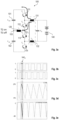
- Fig. 1 show a schematic of the topology of the voltage balancing circuit (100).
- the circuit is based on a converter topology that comprises a DC link consisting of a positive DC capacitor 101 and a negative capacitor 102. In between these capacitors is the midpoint 103.
- Parallel to the DC link 101, 102 a series of switches 111, 112, 113, and 114 are connected.
- the switches 111 and 114 that connect the DC link to the series of switches are referred to as “outer directional devices" or “outer switches”.
- the switches 112 and 113 between the outer switches are referred to as "inner switches”.
- a switch consists of a transistor and an antiparallel freewheeling diode.
- the transistors are designated T1, T2, T3 and T4 corresponding to the switches 111, 112, 113, and 114.
- the inner switches 112, 113 are connected to each other at midpoint 121.
- the DC source 140 may be, here as an example, a battery. Battery 140 is connected over inductances 131 and 132, respectively, to the switches.
- inductance 131 is connected to the connection point of the outer switch 111 and the inner switches 112, and inductance 132 is connected to the connection point of the inner switch 113 and the outer switch 114.
- the particularity in the depicted circuit 100 is the inductance L4 120 that is arranged between the midpoint 103 of the DC link 101, 102 and the midpoint 121 of the inner switches 112, 113.
- the inductance 120 enables the voltage balancing functionality as explained in the following.
- Inductors 131 and 132 as shown are coupled, that is, they are arranged as a single differential choke assembly with separate windings. However, in some embodiments, the windings may be separate.
- Fig. 2a to 2e show the flow of the current in voltage balancing circuit 100 and diagrams of currents and the state of the inner switches during a first switching state.
- Fig. 2b shows the on-state of T2 and Fig. 2c the on-state of T3 corresponding to step S1 802 of the method 800 described herein and depicted in Fig. 8 .
- Fig. 2a shows the flow of the current from the positive pole of the battery through inductance 131, the inner switches 112 and 113, and the inductance 132 to the minus pole 132 of the battery 140. By this flow of the current, the inductivities 131 and 132 are loaded.
- Fig. 2d shows the rise of the current in the inductance 131 connected to the battery 140.
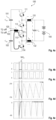
- Fig. 3a to 3e show the flow of the current in voltage balancing circuit 100 and diagrams of currents and the state of the inner switches during a second switching state.
- Fig. 3b shows the on-state of T2 and Fig. 3c the off-state of T3 corresponding to step S2 804 of the method described herein.
- Switching off T3 results in driving the current stored in inductance 131 over the freewheeling diode of switch 111 to the capacitor 101 on one hand and via the closed transistor to inductance 120.
- the current of inductance 131 decreases, whereas the amount of current of inductance 120 increases. Further, the current keeps flowing also through the freewheeling diode of T4 114 and inductor 132.
- Fig. 4a to 4e show the flow of the current in voltage balancing circuit 100 and diagrams of currents and the state of the inner switches during a third switching state.
- Fig. 4b shows the off-state of T2 and Fig. 4c the off-state of T3 corresponding to step S3 806 of the method described herein.
- inductance 120 continues driving the flow of the current over DC capacitor 102 and freewheeling diode 114 and freewheeling diode of switch 114 back to the inductance 120.
- the stored current in 131 flows through the freewheeling diode of switch 111 and decreases therefore further as shown in Fig. 4d , and, which is the point, the current is decreased until zero before the next cycle starts.
- the proposed topology and the delay between switching off T3 and T2 avoid that a voltage peak caused by continued conduction through free wheel diodes of outer switches when both inner switches are closed, that would result in common mode (CM) voltage impressed on the battery terminals.
- CM common mode
- DC voltage balancing may also be obtained by operating the BCB as a 4th Leg converter, when idle that is, driving ON T1 and T2 simultaneously, or T3 and T4 simultaneously, loading the L4 inductor, and leaving it to discharge through the FWD of the opposite pair.
- Fig. 5 shows the differential voltage impressed by voltage balancing circuit bridge.
- the voltage is 850 V if one of T2 or T3 are open and 0 V if T2 and T3 are closed.
- Fig. 6 shows the CM voltage on battery terminals and it can be seen that the CM voltage remains approximately zero as desired.
- Fig. 7 shows the DC link voltage, which has only a slight ripple.
- the ripple is linked to the ratio of the battery voltage to the DC-link voltage.
- the voltage ripple may be reduced by increasing the DC-link capacitance and/or the converter switching frequency.
- Fig. 8 shows a diagram of the method 800 comprising the following steps: In a first step S1, 802: the first and the second switch are switched on. In a second step S2, 804, after a first time interval, the second switch is switched off. In a third step S3, 806, after a further second time interval, the first switch is switched off. In a fourth step, S4, 808, after a further third time interval, it is jumped to S1 802 and the previous steps are repeated.
- a computer program may be stored/distributed on a suitable medium such as an optical storage medium or a solid-state medium supplied together with or as part of other hardware, but may also be distributed in other forms, such as via the Internet or other wired or wireless telecommunication systems. Any reference signs in the claims should not be construed as limiting the scope of the claims.
Landscapes
- Engineering & Computer Science (AREA)
- Power Engineering (AREA)
- Dc-Dc Converters (AREA)
Claims (11)
- Doppel-Boost-DC/DC-Wandler (100), betreibbar in einem Spannungs-Ausgleichsmodus; wobei der Doppel-Boost-DC/DC-Wandler umfasst:eine geteilte DC-Verbindung (101, 102) mit Mittelpunkt (103); äußere Schalter (111, 114) und innere Schalter (112, 113), parallel zur DC-Verbindung (101, 102) geschaltet, wobei die äußeren Schalter mit Kondensatoren der geteilten DC-Verbindung und mit den inneren Schaltern (112, 113) verbunden sind und die inneren Schalter (112, 113) an einem Mittelpunkt (121) miteinander verbunden sind; undein DC-Quellenanschluss, an den eine DC-Quelle (140) parallel zu den inneren Schaltern (112, 113) über Induktivitäten (131, 132) anschließbar ist;die Induktivitäten (131, 132), über die die DC-Quelle (140) parallel zu den inneren Schaltern (112, 113) anschließbar ist;eine Induktivität (120), die mit dem Mittelpunkt (103) der DC-Verbindung und mit dem Mittelpunkt (121) der inneren Schalter (112, 113) verbunden ist; und ein Steuergerät, das dazu eingerichtet ist, die folgenden Schritte auszuführen:in einem ersten Betriebsmodus, der ein Doppel-Boost-Wandler-Modus ist, in dem Strom mit der DC-Quelle ausgetauscht wird:S1 (802): der erste (112) innere und der zweite (113) innere Schalter werden eingeschaltet;S2 (804): nach einem ersten Zeitintervall int1 wird der zweite (113) innere Schalter ausgeschaltet;S3 (806): nach einem weiteren zweiten Zeitintervall int2 wird der erste (112) innere Schalter ausgeschaltet;S4 (808): nach einem weiteren dritten Zeitintervall int3 wird zu S1 (802) zurückgekehrt, wobei die Schaltreihenfolge des ersten und des zweiten inneren Schalters umgekehrt werden kann, so dass S3 vor S2 ausgeführt wird;oder, in einem zweiten Betriebsmodus, der ein Kondensatorspannungs-Ausgleichsmodus ist, in dem kein Strom mit der DC-Quelle ausgetauscht wird,werden der erste äußere Schalter (111) und der erste innere Schalter (112) gleichzeitig mit dem Ausschalten des zweiten äußeren Schalters (114) und des zweiten inneren Schalters (113) eingeschaltet;werden der erste äußere Schalter (111) und der erste innere Schalter (112) gleichzeitig mit dem Einschalten des zweiten äußeren Schalters (114) und des zweiten inneren Schalters (113) ausgeschaltet.
- Doppel-Boost-DC/DC-Wandler (100) nach Anspruch 1, wobei jeder innere Schalter (112, 113) einen Transistor und eine antiparallele Diode umfasst.
- Doppel-Boost-DC/DC-Wandler (100) nach Anspruch 2, wobei jeder äußere Schalter (111, 114) einen Transistor und eine antiparallele Diode umfasst.
- Doppel-Boost-DC/DC-Wandler (100) nach einem der vorhergehenden Ansprüche, wobei die Länge des dritten Zeitintervalls gleich oder größer als das zweite Zeitintervall ist.
- Doppel-Boost-DC/DC-Wandler (100) nach einem der vorhergehenden Ansprüche, wobei die Spannungsausgleichsschaltung (100) ferner die Gleichstromquelle (140) umfasst.
- Doppel-Boost-DC/DC-Wandler (100) nach einem der vorhergehenden Ansprüche, wobei die Gleichstromquelle (140) eine Batterie oder ein Solarpanel ist.
- Doppel-Boost-DC/DC-Wandler nach einem der vorhergehenden Ansprüche, wobei der Doppel-Boost-Wandler als Buck-Boost-Wandler zum Spannungsausgleich der Zwischenkreisspannung betrieben wird, wenn kein Strom mit der Gleichstromquelle (140) ausgetauscht wird.
- Verfahren (800) zum Steuern eines Doppel-Boost-DC/DC-Wandlers (100), wobei der Doppel-Boost-DC/DC-Wandler (100) umfassteine geteilte DC-Verbindung (101, 102) mit Mittelpunkt (103); äußere Schalter (111, 114) und innere Schalter (112, 113), die parallel zur DC-Verbindung (101, 102) geschaltet sind, wobei die äußeren Schalter mit Kondensatoren der geteilten DC-Verbindung und mit den inneren Schaltern (112, 113) verbunden sind und die inneren Schalter (112, 113) an einem Mittelpunkt (121) miteinander verbunden sind; undInduktivitäten (131, 132), über die eine Gleichstromquelle (140) parallel zu den inneren Schaltern (112, 113) angeschlossen ist; eine Induktivität (120), die mit dem Mittelpunkt (103) der DC-Verbindung und mit dem Mittelpunkt (121) der inneren Schalter (112, 113) verbunden ist; undein Steuergerät; wobei das Verfahren von dem Steuergerät durchgeführt wird und in einem ersten Betriebsmodus, der ein Doppel-Boost-Wandler-Modus ist, in dem Strom mit der Gleichstromquelle ausgetauscht wird, das folgenden Schritte umfasst:S1 (802): Der erste (112) und der zweite (113) innere Schalter werden eingeschaltet;S2 (804): Nach einem ersten Zeitintervall int1 wird der zweite (113) innere Schalter ausgeschaltet;S3 (806): Nach einem weiteren zweiten Zeitintervall int2 wird der erste (112) innere Schalter ausgeschaltet;S4 (808): Nach einem weiteren dritten Zeitintervall int3 wird zu S1 (802) zurückgekehrt, wobei die Schaltreihenfolge des ersten und des zweiten inneren Schalters umgekehrt werden kann, so dass S3 vor S2 ausgeführt wird; oder in einem zweiten Betriebsmodus, der ein Kondensatorspannungs-Ausgleichsmodus ist, in dem kein Strom mit der Gleichstromquelle ausgetauscht wird, gleichzeitiges Einschalten des ersten äußeren Schalters (111) und des ersten inneren Schalters (112) bei gleichzeitigem Ausschalten des zweiten äußeren Schalters (114) und des zweiten inneren Schalters (113); gleichzeitiges Ausschalten des ersten äußeren Schalters (111) und des ersten inneren Schalters (112) bei gleichzeitigem Einschalten des zweiten äußeren Schalters (114) und des zweiten inneren Schalters (113).
- Vorrichtung, umfassend einen Doppel-Boost-DC/DC-Wandler (100) nach einem der Ansprüche 1 bis 7, wobei die Vorrichtung eine unterbrechungsfreie Stromversorgung (USV), ein Photovoltaik-/Solarwechselrichter, ein Batteriespeichersystem (BESS) oder ein Wandler ist, der ein DC-Mikronetz mit einem AC-Netz koppelt.
- Verfahren nach Anspruch 8, wobei der Doppel-Boost-DC/DC-Wandler (100) in einer USV, einem Photovoltaik-/Solarwechselrichter, einem Batteriespeichersystem (BESS) oder einem Wandler enthalten ist, der ein DC-Mikronetz mit einem AC-Netz koppelt.
- Programmelement, das, wenn es auf einem Steuergerät in einem Doppel-Boost-DC/DC-Wandler ausgeführt wird, das Steuergerät anweist, die Schritte des Verfahrens nach Anspruch 8 auszuführen.
Priority Applications (3)
| Application Number | Priority Date | Filing Date | Title |
|---|---|---|---|
| EP21172502.3A EP4087113B1 (de) | 2021-05-06 | 2021-05-06 | Doppel-boost-gleichspannungswandler |
| CN202210480256.1A CN115313866A (zh) | 2021-05-06 | 2022-05-05 | 双升压dc/dc转换器 |
| US17/737,158 US12218595B2 (en) | 2021-05-06 | 2022-05-05 | Double-boost DC/DC converter |
Applications Claiming Priority (1)
| Application Number | Priority Date | Filing Date | Title |
|---|---|---|---|
| EP21172502.3A EP4087113B1 (de) | 2021-05-06 | 2021-05-06 | Doppel-boost-gleichspannungswandler |
Publications (2)
| Publication Number | Publication Date |
|---|---|
| EP4087113A1 EP4087113A1 (de) | 2022-11-09 |
| EP4087113B1 true EP4087113B1 (de) | 2025-07-02 |
Family
ID=75825678
Family Applications (1)
| Application Number | Title | Priority Date | Filing Date |
|---|---|---|---|
| EP21172502.3A Active EP4087113B1 (de) | 2021-05-06 | 2021-05-06 | Doppel-boost-gleichspannungswandler |
Country Status (3)
| Country | Link |
|---|---|
| US (1) | US12218595B2 (de) |
| EP (1) | EP4087113B1 (de) |
| CN (1) | CN115313866A (de) |
Families Citing this family (4)
| Publication number | Priority date | Publication date | Assignee | Title |
|---|---|---|---|---|
| DE102022207433A1 (de) * | 2022-07-21 | 2024-02-01 | Zf Friedrichshafen Ag | Symmetrischer Boost-DC/DC-Wandler |
| US12374994B2 (en) * | 2023-01-05 | 2025-07-29 | Infineon Technologies Austria Ag | Constant power buck-boost power converter and methods |
| CN116073647A (zh) * | 2023-03-02 | 2023-05-05 | 湖南大学 | 一种直流变换器及其控制方法 |
| GB2634923A (en) * | 2023-10-25 | 2025-04-30 | Zhuzhou Crrc Times Electric Co Ltd | Dual-boost hardware solution for mitigating neutral point voltage fluctuations |
Family Cites Families (23)
| Publication number | Priority date | Publication date | Assignee | Title |
|---|---|---|---|---|
| US6353547B1 (en) * | 2000-08-31 | 2002-03-05 | Delta Electronics, Inc. | Three-level soft-switched converters |
| TW561680B (en) * | 2001-03-29 | 2003-11-11 | Delta Electronics Inc | Three-level soft-switched converters |
| US7352083B2 (en) | 2005-09-16 | 2008-04-01 | American Power Conversion Corporation | Apparatus for and method of UPS operation |
| US7688048B2 (en) | 2007-02-21 | 2010-03-30 | American Power Conversion Corporation | 3-phase high power UPS |
| CN101090203A (zh) | 2007-07-06 | 2007-12-19 | 艾默生网络能源有限公司 | 在线式不间断ups系统 |
| JP5248611B2 (ja) | 2008-07-30 | 2013-07-31 | 東芝三菱電機産業システム株式会社 | 電力変換装置 |
| WO2010021052A1 (ja) | 2008-08-22 | 2010-02-25 | 東芝三菱電機産業システム株式会社 | 電力変換装置 |
| US8482154B2 (en) | 2009-03-05 | 2013-07-09 | Toshiba Mitsubishi-Electric Industrial Systems Corporation | Uninterruptible power supply apparatus |
| US8513928B2 (en) | 2011-01-05 | 2013-08-20 | Eaton Corporation | Bidirectional buck-boost converter |
| JP5800130B2 (ja) | 2011-06-20 | 2015-10-28 | 富士電機株式会社 | 直流電源システム |
| CN102647083B (zh) * | 2012-04-23 | 2014-05-07 | 淮海工学院 | 一种升压型双向电压平衡变换器 |
| CN103248256A (zh) * | 2013-05-20 | 2013-08-14 | 合肥工业大学 | 具有中点平衡能力的倍压三电平光伏并网逆变器 |
| US10454301B2 (en) | 2014-01-27 | 2019-10-22 | Vertiv S.R.L. | System and method for detecting and correcting DC bus imbalances between parallel coupled UPS systems sharing a common battery |
| EP2975753B1 (de) * | 2014-07-14 | 2021-11-17 | ABB Schweiz AG | Dreistufiger Umrichter |
| WO2016157468A1 (ja) | 2015-04-01 | 2016-10-06 | 東芝三菱電機産業システム株式会社 | 無停電電源装置およびそれを用いた無停電電源システム |
| WO2016157469A1 (ja) | 2015-04-01 | 2016-10-06 | 東芝三菱電機産業システム株式会社 | 無停電電源装置およびそれを用いた無停電電源システム |
| CN205622509U (zh) * | 2016-05-18 | 2016-10-05 | 大连新大路电气传动技术有限责任公司 | 具有电能双向传输功能的机车车辆直流电压变换器 |
| US9935549B2 (en) | 2016-07-08 | 2018-04-03 | Toshiba International Corporation | Multi-switch power converter |
| US10211672B2 (en) | 2016-10-13 | 2019-02-19 | Schneider Electric It Corporation | DC-link bus balancer |
| EP3846329B1 (de) * | 2019-12-31 | 2025-08-06 | Solaredge Technologies Ltd. | Gleichstromausgleichsschaltung mit zvs |
| US11108329B1 (en) * | 2020-02-28 | 2021-08-31 | Astec International Limited | Switch-mode power supplies including three-level LLC circuits for low line and high line operation |
| US11349336B2 (en) * | 2020-03-03 | 2022-05-31 | Delta Electronics, Inc. | Method for operating power factor correction circuit and method for operating uninterruptible power supply apparatus |
| KR20230056079A (ko) * | 2021-10-19 | 2023-04-27 | 한국전자기술연구원 | 양극성 lvdc 배전망 시스템 및 이의 제어 방법 |
-
2021
- 2021-05-06 EP EP21172502.3A patent/EP4087113B1/de active Active
-
2022
- 2022-05-05 CN CN202210480256.1A patent/CN115313866A/zh active Pending
- 2022-05-05 US US17/737,158 patent/US12218595B2/en active Active
Non-Patent Citations (2)
| Title |
|---|
| PATRAO IVÁN ET AL: "Grid-tie inverter topology with maximum power extraction from two photovoltaic arrays", IET RENEWABLE POWER GENERATION, THE INSTITUTION OF ENGINEERING AND TECHNOLOGY, MICHAEL FARADAY HOUSE, SIX HILLS WAY, STEVENAGE, HERTS. SG1 2AY, UK, vol. 8, no. 6, 1 August 2014 (2014-08-01), pages 638 - 648, XP006049119, ISSN: 1752-1416, DOI: 10.1049/IET-RPG.2013.0143 * |
| RIVERA SEBASTIAN ET AL: "Bipolar DC Power Conversion: State-of-the-Art and Emerging Technologies", IEEE JOURNAL OF EMERGING AND SELECTED TOPICS IN POWER ELECTRONICS, IEEE, PISCATAWAY, NJ, USA, vol. 9, no. 2, 16 March 2020 (2020-03-16), pages 1192 - 1204, XP011843801, ISSN: 2168-6777, [retrieved on 20210312], DOI: 10.1109/JESTPE.2020.2980994 * |
Also Published As
| Publication number | Publication date |
|---|---|
| US12218595B2 (en) | 2025-02-04 |
| CN115313866A (zh) | 2022-11-08 |
| US20220360176A1 (en) | 2022-11-10 |
| EP4087113A1 (de) | 2022-11-09 |
Similar Documents
| Publication | Publication Date | Title |
|---|---|---|
| EP3657661B1 (de) | Wandlungsschaltung, steuerverfahren und energieversorgungsvorrichtung | |
| Nami et al. | Five level cross connected cell for cascaded converters | |
| JP5457449B2 (ja) | 電力変換装置 | |
| JP5059879B2 (ja) | 三相で高電力の無停電電源 | |
| JP5928928B2 (ja) | 5段階電力変換器ならびにその制御方法および制御装置 | |
| US12218595B2 (en) | Double-boost DC/DC converter | |
| JP5346749B2 (ja) | 電力変換装置 | |
| CN104065280A (zh) | 用于多级逆变器的改进了的电力单元旁通方法及装置 | |
| EP3633843B1 (de) | Stromwandler und ansteuerverfahren dafür | |
| CN105874703A (zh) | 具有软开关切换的逆变器和方法 | |
| US8248828B2 (en) | Medium voltage inverter system | |
| JP5362657B2 (ja) | 電力変換装置 | |
| CN114204836A (zh) | 一种逆变器和逆变装置 | |
| KR20230151479A (ko) | 스위칭 커패시터를 구비한 일반화된 멀티레벨 컨버터 회로 토폴로지 | |
| Hota et al. | Novel boost inverter configuration and 3-ϕ induction motor drive for home appliances | |
| US20240333124A1 (en) | Balancer Circuit for Series Connection of Two DC-Link Capacitors, Method for Controlling the Balancer Circuit and Converter Arrangement | |
| Tran et al. | Space vector modulation scheme for three-level T-type quasi-switched boost inverter to reduce common mode voltage | |
| Sekhar et al. | Novel multilevel inverter with minimum number of switches | |
| Bharath et al. | A Novel 1-ϕ, 5-level transformerless inverter with voltage boosting capability | |
| JP2016149888A (ja) | 電力変換装置 | |
| Padilha et al. | Low-cost gate drive circuit for three-level neutral-point-clamped voltage-source inverter | |
| Sandeep et al. | Switched-capacitor-based three-phase five-level inverter topology with reduced components | |
| CN117730476A (zh) | 具有多种运行模式的基于单元的多电平转换器和相关联的控制方法 | |
| Cheng et al. | The topology analysis and compare of high-frequency power electronic transformer | |
| JP2014124025A (ja) | インバータ装置のスイッチング素子駆動電源回路 |
Legal Events
| Date | Code | Title | Description |
|---|---|---|---|
| PUAI | Public reference made under article 153(3) epc to a published international application that has entered the european phase |
Free format text: ORIGINAL CODE: 0009012 |
|
| STAA | Information on the status of an ep patent application or granted ep patent |
Free format text: STATUS: THE APPLICATION HAS BEEN PUBLISHED |
|
| AK | Designated contracting states |
Kind code of ref document: A1 Designated state(s): AL AT BE BG CH CY CZ DE DK EE ES FI FR GB GR HR HU IE IS IT LI LT LU LV MC MK MT NL NO PL PT RO RS SE SI SK SM TR |
|
| STAA | Information on the status of an ep patent application or granted ep patent |
Free format text: STATUS: REQUEST FOR EXAMINATION WAS MADE |
|
| 17P | Request for examination filed |
Effective date: 20230505 |
|
| RBV | Designated contracting states (corrected) |
Designated state(s): AL AT BE BG CH CY CZ DE DK EE ES FI FR GB GR HR HU IE IS IT LI LT LU LV MC MK MT NL NO PL PT RO RS SE SI SK SM TR |
|
| STAA | Information on the status of an ep patent application or granted ep patent |
Free format text: STATUS: EXAMINATION IS IN PROGRESS |
|
| 17Q | First examination report despatched |
Effective date: 20230728 |
|
| GRAP | Despatch of communication of intention to grant a patent |
Free format text: ORIGINAL CODE: EPIDOSNIGR1 |
|
| STAA | Information on the status of an ep patent application or granted ep patent |
Free format text: STATUS: GRANT OF PATENT IS INTENDED |
|
| INTG | Intention to grant announced |
Effective date: 20250326 |
|
| GRAS | Grant fee paid |
Free format text: ORIGINAL CODE: EPIDOSNIGR3 |
|
| GRAA | (expected) grant |
Free format text: ORIGINAL CODE: 0009210 |
|
| STAA | Information on the status of an ep patent application or granted ep patent |
Free format text: STATUS: THE PATENT HAS BEEN GRANTED |
|
| AK | Designated contracting states |
Kind code of ref document: B1 Designated state(s): AL AT BE BG CH CY CZ DE DK EE ES FI FR GB GR HR HU IE IS IT LI LT LU LV MC MK MT NL NO PL PT RO RS SE SI SK SM TR |
|
| REG | Reference to a national code |
Ref country code: GB Ref legal event code: FG4D |
|
| REG | Reference to a national code |
Ref country code: CH Ref legal event code: EP |
|
| REG | Reference to a national code |
Ref country code: DE Ref legal event code: R096 Ref document number: 602021033188 Country of ref document: DE |
|
| REG | Reference to a national code |
Ref country code: IE Ref legal event code: FG4D |
|
| REG | Reference to a national code |
Ref country code: NL Ref legal event code: MP Effective date: 20250702 |
|
| PG25 | Lapsed in a contracting state [announced via postgrant information from national office to epo] |
Ref country code: PT Free format text: LAPSE BECAUSE OF FAILURE TO SUBMIT A TRANSLATION OF THE DESCRIPTION OR TO PAY THE FEE WITHIN THE PRESCRIBED TIME-LIMIT Effective date: 20251103 |
|
| PG25 | Lapsed in a contracting state [announced via postgrant information from national office to epo] |
Ref country code: NL Free format text: LAPSE BECAUSE OF FAILURE TO SUBMIT A TRANSLATION OF THE DESCRIPTION OR TO PAY THE FEE WITHIN THE PRESCRIBED TIME-LIMIT Effective date: 20250702 |
|
| REG | Reference to a national code |
Ref country code: AT Ref legal event code: MK05 Ref document number: 1810429 Country of ref document: AT Kind code of ref document: T Effective date: 20250702 |
|
| PG25 | Lapsed in a contracting state [announced via postgrant information from national office to epo] |
Ref country code: IS Free format text: LAPSE BECAUSE OF FAILURE TO SUBMIT A TRANSLATION OF THE DESCRIPTION OR TO PAY THE FEE WITHIN THE PRESCRIBED TIME-LIMIT Effective date: 20251102 |
|
| PG25 | Lapsed in a contracting state [announced via postgrant information from national office to epo] |
Ref country code: NO Free format text: LAPSE BECAUSE OF FAILURE TO SUBMIT A TRANSLATION OF THE DESCRIPTION OR TO PAY THE FEE WITHIN THE PRESCRIBED TIME-LIMIT Effective date: 20251002 |
|
| REG | Reference to a national code |
Ref country code: LT Ref legal event code: MG9D |
|
| PG25 | Lapsed in a contracting state [announced via postgrant information from national office to epo] |
Ref country code: AT Free format text: LAPSE BECAUSE OF FAILURE TO SUBMIT A TRANSLATION OF THE DESCRIPTION OR TO PAY THE FEE WITHIN THE PRESCRIBED TIME-LIMIT Effective date: 20250702 |
|
| PG25 | Lapsed in a contracting state [announced via postgrant information from national office to epo] |
Ref country code: FI Free format text: LAPSE BECAUSE OF FAILURE TO SUBMIT A TRANSLATION OF THE DESCRIPTION OR TO PAY THE FEE WITHIN THE PRESCRIBED TIME-LIMIT Effective date: 20250702 |
|
| PG25 | Lapsed in a contracting state [announced via postgrant information from national office to epo] |
Ref country code: HR Free format text: LAPSE BECAUSE OF FAILURE TO SUBMIT A TRANSLATION OF THE DESCRIPTION OR TO PAY THE FEE WITHIN THE PRESCRIBED TIME-LIMIT Effective date: 20250702 |
|
| PG25 | Lapsed in a contracting state [announced via postgrant information from national office to epo] |
Ref country code: GR Free format text: LAPSE BECAUSE OF FAILURE TO SUBMIT A TRANSLATION OF THE DESCRIPTION OR TO PAY THE FEE WITHIN THE PRESCRIBED TIME-LIMIT Effective date: 20251003 |
|
| PG25 | Lapsed in a contracting state [announced via postgrant information from national office to epo] |
Ref country code: SE Free format text: LAPSE BECAUSE OF FAILURE TO SUBMIT A TRANSLATION OF THE DESCRIPTION OR TO PAY THE FEE WITHIN THE PRESCRIBED TIME-LIMIT Effective date: 20250702 Ref country code: CZ Free format text: LAPSE BECAUSE OF FAILURE TO SUBMIT A TRANSLATION OF THE DESCRIPTION OR TO PAY THE FEE WITHIN THE PRESCRIBED TIME-LIMIT Effective date: 20250702 |
|
| PG25 | Lapsed in a contracting state [announced via postgrant information from national office to epo] |
Ref country code: LV Free format text: LAPSE BECAUSE OF FAILURE TO SUBMIT A TRANSLATION OF THE DESCRIPTION OR TO PAY THE FEE WITHIN THE PRESCRIBED TIME-LIMIT Effective date: 20250702 |
|
| PG25 | Lapsed in a contracting state [announced via postgrant information from national office to epo] |
Ref country code: PL Free format text: LAPSE BECAUSE OF FAILURE TO SUBMIT A TRANSLATION OF THE DESCRIPTION OR TO PAY THE FEE WITHIN THE PRESCRIBED TIME-LIMIT Effective date: 20250702 Ref country code: BG Free format text: LAPSE BECAUSE OF FAILURE TO SUBMIT A TRANSLATION OF THE DESCRIPTION OR TO PAY THE FEE WITHIN THE PRESCRIBED TIME-LIMIT Effective date: 20250702 |
|
| PG25 | Lapsed in a contracting state [announced via postgrant information from national office to epo] |
Ref country code: RS Free format text: LAPSE BECAUSE OF FAILURE TO SUBMIT A TRANSLATION OF THE DESCRIPTION OR TO PAY THE FEE WITHIN THE PRESCRIBED TIME-LIMIT Effective date: 20251002 |
|
| PG25 | Lapsed in a contracting state [announced via postgrant information from national office to epo] |
Ref country code: ES Free format text: LAPSE BECAUSE OF FAILURE TO SUBMIT A TRANSLATION OF THE DESCRIPTION OR TO PAY THE FEE WITHIN THE PRESCRIBED TIME-LIMIT Effective date: 20250702 |
|
| PG25 | Lapsed in a contracting state [announced via postgrant information from national office to epo] |
Ref country code: SM Free format text: LAPSE BECAUSE OF FAILURE TO SUBMIT A TRANSLATION OF THE DESCRIPTION OR TO PAY THE FEE WITHIN THE PRESCRIBED TIME-LIMIT Effective date: 20250702 |
|
| PG25 | Lapsed in a contracting state [announced via postgrant information from national office to epo] |
Ref country code: DK Free format text: LAPSE BECAUSE OF FAILURE TO SUBMIT A TRANSLATION OF THE DESCRIPTION OR TO PAY THE FEE WITHIN THE PRESCRIBED TIME-LIMIT Effective date: 20250702 |
|
| PG25 | Lapsed in a contracting state [announced via postgrant information from national office to epo] |
Ref country code: SK Free format text: LAPSE BECAUSE OF FAILURE TO SUBMIT A TRANSLATION OF THE DESCRIPTION OR TO PAY THE FEE WITHIN THE PRESCRIBED TIME-LIMIT Effective date: 20250702 Ref country code: EE Free format text: LAPSE BECAUSE OF FAILURE TO SUBMIT A TRANSLATION OF THE DESCRIPTION OR TO PAY THE FEE WITHIN THE PRESCRIBED TIME-LIMIT Effective date: 20250702 |
|
| PLBE | No opposition filed within time limit |
Free format text: ORIGINAL CODE: 0009261 |
|
| STAA | Information on the status of an ep patent application or granted ep patent |
Free format text: STATUS: NO OPPOSITION FILED WITHIN TIME LIMIT |