EP4087123A1 - Oszillatorschaltungen - Google Patents
Oszillatorschaltungen Download PDFInfo
- Publication number
- EP4087123A1 EP4087123A1 EP22171342.3A EP22171342A EP4087123A1 EP 4087123 A1 EP4087123 A1 EP 4087123A1 EP 22171342 A EP22171342 A EP 22171342A EP 4087123 A1 EP4087123 A1 EP 4087123A1
- Authority
- EP
- European Patent Office
- Prior art keywords
- resonator
- voltage
- buffer
- resonance
- circuit
- Prior art date
- Legal status (The legal status is an assumption and is not a legal conclusion. Google has not performed a legal analysis and makes no representation as to the accuracy of the status listed.)
- Pending
Links
Images


Classifications
-
- H—ELECTRICITY
- H03—ELECTRONIC CIRCUITRY
- H03B—GENERATION OF OSCILLATIONS, DIRECTLY OR BY FREQUENCY-CHANGING, BY CIRCUITS EMPLOYING ACTIVE ELEMENTS WHICH OPERATE IN A NON-SWITCHING MANNER; GENERATION OF NOISE BY SUCH CIRCUITS
- H03B5/00—Generation of oscillations using amplifier with regenerative feedback from output to input
- H03B5/30—Generation of oscillations using amplifier with regenerative feedback from output to input with frequency-determining element being electromechanical resonator
- H03B5/32—Generation of oscillations using amplifier with regenerative feedback from output to input with frequency-determining element being electromechanical resonator being a piezoelectric resonator
- H03B5/36—Generation of oscillations using amplifier with regenerative feedback from output to input with frequency-determining element being electromechanical resonator being a piezoelectric resonator active element in amplifier being semiconductor device
-
- H—ELECTRICITY
- H03—ELECTRONIC CIRCUITRY
- H03B—GENERATION OF OSCILLATIONS, DIRECTLY OR BY FREQUENCY-CHANGING, BY CIRCUITS EMPLOYING ACTIVE ELEMENTS WHICH OPERATE IN A NON-SWITCHING MANNER; GENERATION OF NOISE BY SUCH CIRCUITS
- H03B5/00—Generation of oscillations using amplifier with regenerative feedback from output to input
- H03B5/02—Details
- H03B5/06—Modifications of generator to ensure starting of oscillations
-
- H—ELECTRICITY
- H03—ELECTRONIC CIRCUITRY
- H03B—GENERATION OF OSCILLATIONS, DIRECTLY OR BY FREQUENCY-CHANGING, BY CIRCUITS EMPLOYING ACTIVE ELEMENTS WHICH OPERATE IN A NON-SWITCHING MANNER; GENERATION OF NOISE BY SUCH CIRCUITS
- H03B5/00—Generation of oscillations using amplifier with regenerative feedback from output to input
- H03B5/30—Generation of oscillations using amplifier with regenerative feedback from output to input with frequency-determining element being electromechanical resonator
- H03B5/32—Generation of oscillations using amplifier with regenerative feedback from output to input with frequency-determining element being electromechanical resonator being a piezoelectric resonator
- H03B5/36—Generation of oscillations using amplifier with regenerative feedback from output to input with frequency-determining element being electromechanical resonator being a piezoelectric resonator active element in amplifier being semiconductor device
- H03B5/364—Generation of oscillations using amplifier with regenerative feedback from output to input with frequency-determining element being electromechanical resonator being a piezoelectric resonator active element in amplifier being semiconductor device the amplifier comprising field effect transistors
-
- H—ELECTRICITY
- H03—ELECTRONIC CIRCUITRY
- H03L—AUTOMATIC CONTROL, STARTING, SYNCHRONISATION OR STABILISATION OF GENERATORS OF ELECTRONIC OSCILLATIONS OR PULSES
- H03L7/00—Automatic control of frequency or phase; Synchronisation
- H03L7/06—Automatic control of frequency or phase; Synchronisation using a reference signal applied to a frequency- or phase-locked loop
- H03L7/08—Details of the phase-locked loop
- H03L7/099—Details of the phase-locked loop concerning mainly the controlled oscillator of the loop
-
- H—ELECTRICITY
- H03—ELECTRONIC CIRCUITRY
- H03B—GENERATION OF OSCILLATIONS, DIRECTLY OR BY FREQUENCY-CHANGING, BY CIRCUITS EMPLOYING ACTIVE ELEMENTS WHICH OPERATE IN A NON-SWITCHING MANNER; GENERATION OF NOISE BY SUCH CIRCUITS
- H03B2200/00—Indexing scheme relating to details of oscillators covered by H03B
- H03B2200/006—Functional aspects of oscillators
- H03B2200/0082—Lowering the supply voltage and saving power
-
- H—ELECTRICITY
- H03—ELECTRONIC CIRCUITRY
- H03B—GENERATION OF OSCILLATIONS, DIRECTLY OR BY FREQUENCY-CHANGING, BY CIRCUITS EMPLOYING ACTIVE ELEMENTS WHICH OPERATE IN A NON-SWITCHING MANNER; GENERATION OF NOISE BY SUCH CIRCUITS
- H03B2200/00—Indexing scheme relating to details of oscillators covered by H03B
- H03B2200/006—Functional aspects of oscillators
- H03B2200/0094—Measures to ensure starting of oscillations
Definitions
- the present invention relates to oscillator circuits and methods of operating oscillator circuits.
- a common form of oscillator circuit is a crystal oscillator circuit, which comprises a piezoelectric crystal resonator (usually made of quartz) and a driving amplifier, which has its output fed back into its input via the crystal resonator.
- the crystal resonator acts as a very narrow filter, causing the circuit to oscillate at or near the resonant frequency of the crystal.
- Crystal resonators generally have a high Q factor and good temperature stability, which means they can be used to produce very stable clock signals.
- crystal oscillator circuits typically require much more power to operate than equivalent non-crystal oscillators (e.g. an LC oscillator where a tuned LC circuit replaces the crystal), due to bias current losses in the driving amplifier (which is always powered), resistive losses in the rest of the circuit and power loss due to the piezoelectric movement of the crystal itself.
- equivalent non-crystal oscillators e.g. an LC oscillator where a tuned LC circuit replaces the crystal
- bias current losses in the driving amplifier which is always powered
- resistive losses in the rest of the circuit resistive losses in the rest of the circuit
- power loss due to the piezoelectric movement of the crystal itself.
- an LC oscillator circuit might consume less than 1% of the power of an equivalent crystal oscillator circuit (albeit whilst providing less accurate timing).
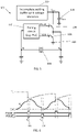
- Figure 1 shows a pulse injection crystal oscillator 2 (or PIXO) according to the prior art, in which a piezoelectric crystal 4 is alternately connected to a supply voltage rail 6 and a ground rail 8 for only short pulses (e.g. on the order of microseconds), at a rate locked to the resonance of the crystal using a timing circuit 10.
- the operation of the PIXO 2 is illustrated in Figure 2 , from which it can be seen that the voltage at node Xo oscillates between the voltage V DDL of the supply voltage rail 6 and that of the ground rail 8.
- the crystal 4 is connected to the supply voltage rail 6 for a short period of time to charge the crystal 4 to the supply voltage V DDL .
- the crystal is connected to ground 8 for another short period of time to discharge the crystal 4.
- the supply voltage rail must be generated by sufficiently powerful circuitry to fully charge the crystal and its large load capacitance (e.g. typically more than 10 pF) during the short pulses.
- the instantaneous power requirements are relatively high, which can increase the cost and size of the PIXO or supporting circuitry.
- a switched capacitor network with several very large capacitors may be needed to generate the voltage rail.
- a method of operating an oscillator circuit comprising a resonator, the method comprising maintaining a resonance of the resonator by:
- an oscillator circuit comprising a resonator, wherein the oscillator circuit is arranged to maintain a resonance of the resonator by:
- the oscillator circuit by driving the oscillator by only partially charging the resonator towards the input voltage in regular pulses (i.e. incomplete settling pulse injection), the instantaneous power demand of the oscillator circuit may be reduced.
- the Applicant has recognised that by partially charging the resonator consistently by repeatedly connecting it to the input voltage for the first pulse period, the oscillator circuit can still provide accurate timing but with reduced power consumption and a reduced instantaneous power demand. Power supply components with a smaller bandwidth may be used, reducing the size and/or cost of the oscillator circuit.
- the present invention may be used with many different types of resonator, such as electronic circuits (e.g. an RC circuit or a tuned LC circuit) or dielectric resonators.
- the resonator comprises a piezoelectric material, for instance a quartz crystal.
- Piezoelectric resonators typically have a high Q factor and good temperature stability, allowing for excellent frequency stability.
- piezoelectric resonators can require more power to operate than other types of resonator, thus making them particularly suited to the power-saving benefits which may be achieved in accordance with the present invention.
- the resonance of the resonator may occur at exactly an inherent resonant frequency of the resonator (e.g. a series resonant frequency). However in some embodiments it may be appropriate to maintain the resonance of the resonator at a slightly higher, or a slightly lower frequency near to the inherent resonant frequency.
- the steps a) and b) are repeated at a rate corresponding to the resonance of the resonator. This may comprise repeating steps a) and b) at a rate that is equal or near to the frequency of the resonance of the resonator. However the steps a) and b) may alternatively be repeated at a rate equal or near to an integer multiple or division of the frequency of the resonance of the resonator.
- the steps a) and b) are repeated with a phase corresponding to the resonance of the resonator, e.g. the first and second pulse periods are phase-locked (i.e. having a fixed phase relationship) to the resonance of the resonator with appropriate phase relationships for maintaining the resonance.
- This may comprise repeating step a) at or close to a peak of the resonance (e.g. approximately 90 degrees out of phase with a sinusoidal resonance of the resonator), and/or repeating step b) at or close to a lowest point of the resonance (e.g. approximately 270 degrees out of phase with a sinusoidal resonance of the resonator).
- the resonator is charged in the first pulse period only partially towards the input voltage. In a set of embodiments it is charged to less than 80% of the input voltage, e.g. less than 65% of the input voltage, e.g. between 35% and 62% of the input voltage.
- the oscillator circuit comprises a buffer circuit arranged to provide the input voltage, i.e. such that the input voltage comprises a buffer voltage provided by the buffer circuit.
- the buffer circuit may comprise a voltage buffer.
- the buffer circuit may be arranged simply to transfer a supply voltage of the oscillator circuit, or an offset version of the supply voltage, as the buffer voltage. This may comprise a simple implementation of the buffer circuit.
- the buffer circuit may be arranged to generate a reference voltage and transfer this reference voltage (or an offset version thereof) as the buffer voltage.
- the reference voltage may be lower than a supply voltage of the oscillator circuit.
- the buffer circuit may comprise a reference voltage portion arranged to generate a reference voltage that is substantially insensitive to temperature.
- the reference voltage portion may comprise one or more transistors arranged as a beta-multiplier circuit.
- the reference voltage portion may comprise a reference resistor, the resistance of which may be selected to achieve a desired reference voltage.
- the reference voltage portion may comprise a bias resistor arranged to offset the reference voltage.
- the bias resistor may comprise an adjustable bias resistor, e.g. to allow the reference voltage to be optimised for use with different resonators (e.g. crystals with different properties).
- the buffer circuit may comprise a buffer portion arranged simply to transfer the reference voltage or an offset version of the reference voltage as the buffer voltage.
- the buffer portion may comprise a source follower transistor that has its gate terminal connected to the reference voltage (or an offset version thereof), and its drain terminal connected to a supply voltage of the oscillator circuit.
- the use of a source follower transistor may enable the buffer circuit to deliver more current to the resonator than its DC bias when the buffer voltage drops (i.e. on connection to the resonator in the first pulse period).
- the buffer circuit may operate as a class-AB buffer amplifier.
- One or more component transistors of the voltage reference portion and the buffer portion of the buffer circuit may be matched (i.e. selected to have similar or identical characteristics to a greater extent than would be achieved through random selection of the components).
- the oscillator circuit comprises a buffer capacitor that is connected to the resonator during the first pulse period.
- the buffer capacitor may form part of the buffer circuit.
- the buffer capacitor may act as a charge reservoir, storing charge between the first pulse periods and then delivering this charge to the resonator in the first pulse periods. This may further reduce the peak current demand on power supply components, as at least some of the charge required to partially charge the resonator in the first pulse period is provided by the buffer capacitor, reducing the charge that the power supply components need to deliver during the first pulse period.
- the buffer capacitor may be recharged between the first pulse periods.
- the buffer capacitor may be permanently connected between the input voltage and a lower voltage (e.g. the second voltage or a ground voltage), such that it is charged to or towards the input voltage between the first pulse periods, and connected to the resonator to deliver the stored charge thereto during the first pulse periods.
- a lower voltage e.g. the second voltage or a ground voltage
- the charge delivered by the buffer capacitor during the first pulse period may be provided gradually to the capacitor between the first pulse periods, i.e. requiring only a small charging current.
- the buffer capacitor may provide most or even all of the charge required to partially charge the resonator during the first pulse period.
- the buffer capacitor may be able to deliver the charge required to partially charge the resonator very quickly, potentially allowing the duration of the first pulse period to be reduced. This may further reducing the overall power consumption of the oscillator circuit.
- Embodiments featuring a buffer circuit that charges the buffer capacitor between the first pulse periods enable the buffer circuit to do useful work throughout the entire cycle of the resonator.
- the buffer capacitor may have a capacitance that is less than, and possibly significantly less than, a load capacitance of the resonator, so as to charge the resonator only partially during the first pulse period.
- the buffer capacitor may have a capacitance of less than 5 pF, e.g. 1,.4 pF.
- a typical crystal resonator may comprise more than 10 pF of load capacitance per side.
- the oscillator circuit comprises a timing circuit arranged to time the first and second pulse periods (i.e. to ensure they repeat at a rate corresponding to the resonance of the resonator, and with a phase corresponding to the resonance of the resonator).
- the timing circuit may comprise a feedback loop arranged to synchronise the first and second pulse periods with the resonance of the resonator.
- the timing circuit may be arranged to receive a resonance signal from the resonator as an input and to control the timing of the first and second pulse periods to correspond with the resonance signal.
- the timing circuit may comprise a phase locked loop or a delay locked loop.
- Some embodiments may comprise providing an initial resonance signal to start oscillations of the oscillator circuit from an initial zero oscillation state (i.e. a start-up signal to cold-start the oscillator circuit).
- the initial resonance signal may be provided from an external source, but in at least some embodiments the oscillator circuit comprises a start-up circuit arranged to provide an initial resonance signal to initiate operation of the oscillator circuit.
- the start-up circuit may comprise a Pierce oscillator.
- Providing an initial resonance signal to start-up the resonance may be particularly beneficial in embodiments where the timing of steps a) and b) is controlled using the resonance of the resonator itself (e.g. embodiments featuring a timing circuit that receives a resonance signal from the resonator as an input).
- the first pulse period may have a duration on the order of microseconds.
- the first and second pulse periods may have approximately or fully equal durations. This may simplify the circuitry required to time the first and second pulse periods, e.g. allowing common timing components to be used to time the first and second pulse periods.
- the first and second pulse periods may have different durations. This may allow for the power consumption and/or size of the oscillator circuit to be further optimised. For instance, the first pulse period may be longer than the second pulse period, e.g. where circuitry used to discharge the resonator has a higher bandwidth than the circuitry used to charge the resonator. Conversely, the first pulse period may be shorter than the second pulse period.
- Figure 3 shows a pulse injection crystal oscillator circuit 102 that comprises a piezoelectric crystal resonator 104, a buffer circuit 107, and a timing circuit 110.
- the timing circuit 110 alternately connects the crystal resonator 104 to the buffer circuit 107 using a high switch 109 and to a ground rail 108 using a low switch 111, at a rate that corresponds to a resonance of the crystal resonator 104, and with a phase corresponding to the resonance of the resonator.
- the timing circuit 110 is locked to the resonance of the crystal resonator 104 (e.g. using a phase locked loop).
- the timing circuit 110 connects the crystal resonator 104 to a buffer voltage V BUF generated by the buffer circuit 107 for a first pulse period 112.
- the current provided by the buffer circuit 107 charges the crystal resonator 104 partially, but not completely, towards the buffer voltage V BUF (e.g. to between 35% and 62% of V BUF ). Because the crystal resonator 104 is only partially charged towards the buffer voltage V BUF , the charging current provided by the buffer circuit 107 can be relatively small.
- the timing circuit 110 connects the crystal resonator 104 to the ground rail 108 for a second pulse period 114.
- the crystal resonator 104 is completely discharged in the second pulse period 114, this is not essential.
- Figure 4 shows the first and second pulse periods 112, 114 as equal, but again this is not essential.
- the second pulse period 114 may be shorter than the first pulse period 112.
- the duration of the first pulse period 112, and the current bandwidth of the buffer circuit 107 are chosen to ensure that the charge delivered to the crystal resonator 104 is sufficient to keep the oscillation going, whilst minimising the physical size of the buffer 107 and the overall power consumption of the oscillator circuit 102.
- the output X i of the crystal resonator 104 is connected to the timing circuit 110, which controls the process to repeat at a rate corresponding to the resonance of the crystal resonator 104 and phase-locked with the resonance of the crystal resonator 104 (i.e. with the first pules period 112 occurring at or close to the peak of the oscillation waveform, and the second pulse period 114 occurring at or close to the bottom of the oscillation waveform).
- the first and second pulse periods 112, 114 repeat at a rate slightly above the inherent resonant frequency of the crystal resonator 104.
- the timing circuit 110 may, for instance, comprise a phase locked loop (PLL).
- the pulse injection crystal oscillator circuit 102 is shown in Figure 5 .
- the pulse injection crystal oscillator circuit 102 additionally comprises a buffer capacitor 116.
- the buffer capacitor 116 may be considered to form part of the buffer circuit 107.
- the timing circuit 110 is locked to the resonance of the crystal resonator 104 (e.g. because it comprises a phase locked loop).
- the timing circuit 110 closes the high switch 109 to connect the crystal resonator 104 to a buffer voltage V BUF generated by the buffer circuit 107 for a first pulse period 112.
- Charge stored in the buffer capacitor 116 is quickly delivered to the crystal resonator 104, which quickly raises the voltage at node Xo partially towards the buffer voltage V BUF .
- Figure 6 shows that after this initial rise the buffer circuit 107 continues to charge the crystal resonator 104 towards the buffer voltage at a slower rate.
- the timing circuit 110 opens the high switch 109 to disconnect the crystal resonator 104 from the buffer voltage V BUF , and the buffer circuit 107 begins to gradually recharge the buffer capacitor 116 back to the buffer voltage V BUF .
- the timing circuit 110 closes the low switch 111 to connect the crystal resonator 104 to the ground rail 108 for a second pulse period 114.
- the crystal resonator 104 is completely discharged in the second pulse period 114, this is not essential.
- Figure 4 shows the first and second pulse periods 112, 114 as equal, but again this is not essential.
- the second pulse period 114 may be shorter than the first pulse period 112.
- the use of the buffer capacitor 116 allows charge to be quickly delivered to the crystal resonator 104 in the first pulse period 112. Although this is not shown in Figure 6 , this may allow the duration of the first pulse period 112 to be reduced compared to the embodiment described with reference to Figure 4 . This can further reduce the overall power use of the oscillator circuit 102.
- the peak current delivery required of the buffer circuit 107 can be further reduced in this embodiment because it does useful work charging the buffer capacitor 116 throughout the entire resonant cycle before the first pulse period 112 occurs again.
- Figure 6 shows how the buffer circuit 107 gradually recharges the buffer capacitor 116. This may allow the physical size and cost of the buffer circuit 107 to be even further reduced.
- FIG. 7 shows a detailed schematic diagram of the buffer circuit 107.
- the buffer circuit 107 comprises an input voltage rail 158 (which is at voltage V DD ) and a ground rail 108 (at voltage Vss).
- the buffer circuit 107 comprises three portions: a current/voltage reference portion 152, a buffer portion 154 and a switching portion 156. Some or all of the portions 152, 154, 156 may be physically separate (e.g. all the portions of the buffer circuit 107 may not be located on a single integrated circuit).
- the current/voltage reference portion 152 comprises a startup circuit 162, transistors M 1 -M 4 , a reference resistor 166 (with resistance R REF ), and a trim resistor 168 (with resistance R TRIM ).
- the current/voltage reference portion 152 is configured as a beta-multiplier circuit.
- the buffer portion 154 comprises a source follower transistor M 5 and a biasing transistor M 6 .
- the switching portion 156 comprises the high switch 109, which comprises a first switching transistor M 7 arranged to connect the crystal resonator 104 to the buffer voltage V BUF , and the low switch 111, which comprises a second switching transistor M 8 arranged to connect the crystal resonator 104 to the ground rail 108.
- the buffer circuit 107 further comprises the buffer capacitor 116, connected between the source of the first switching transistor M 7 (i.e. the output of the buffer portion 154) and the ground rail 108.
- the first and second switching transistors M 7 , M 8 are controlled by pulses from the timing circuit 110.
- the current/voltage reference portion 152 In use, the current/voltage reference portion 152 generates a reference voltage V REF .
- the bias current generated by the current/voltage reference portion is set by the relative sizing of the transistors M 3-4 and the resistance R REF of the reference resistor 166.
- the reference voltage V REF may be made to be temperature independent
- the startup circuit 162 ensures that the current/voltage reference portion produces the reference voltage V REF rather than an alternative steady-state where zero current flows.
- the buffer portion 154 operates as a voltage buffer.
- V REF is copied to V BUF , offset by the voltage drop across R TRIM .
- the configuration of the buffer circuit 107 ensures that V BUF is generated with acceptable PVT robustness (i.e. the buffer voltage is largely independent of variations in the manufacturing process, the supply voltage Vss and the temperature).
- V BUF the buffer voltage is largely independent of variations in the manufacturing process, the supply voltage Vss and the temperature.
- the buffer portion 154 By configuring the buffer portion 154 as a source follower connected directly to the voltage supply rail 158, it can supply more current than its DC bias when V BUF drops (i.e. acting as an AB-like amplifier), meaning that the bias current consumed by the buffer can be further reduced.
- the bias current in each branch of the buffer circuit 107 is about 2.5 nA, meaning that the whole circuit uses only 7.5 nA of bias current.
Landscapes
- Oscillators With Electromechanical Resonators (AREA)
Applications Claiming Priority (1)
| Application Number | Priority Date | Filing Date | Title |
|---|---|---|---|
| GB202106467 | 2021-05-06 |
Publications (1)
| Publication Number | Publication Date |
|---|---|
| EP4087123A1 true EP4087123A1 (de) | 2022-11-09 |
Family
ID=81580233
Family Applications (1)
| Application Number | Title | Priority Date | Filing Date |
|---|---|---|---|
| EP22171342.3A Pending EP4087123A1 (de) | 2021-05-06 | 2022-05-03 | Oszillatorschaltungen |
Country Status (3)
| Country | Link |
|---|---|
| US (1) | US11764730B2 (de) |
| EP (1) | EP4087123A1 (de) |
| CN (1) | CN115314007A (de) |
Cited By (1)
| Publication number | Priority date | Publication date | Assignee | Title |
|---|---|---|---|---|
| US12549131B2 (en) | 2023-06-22 | 2026-02-10 | Nordic Semiconductor Asa | Switched oscillator circuit |
Families Citing this family (1)
| Publication number | Priority date | Publication date | Assignee | Title |
|---|---|---|---|---|
| US12542516B2 (en) * | 2024-04-10 | 2026-02-03 | Silicon Laboratories Inc. | Crystal oscillator energy injection |
Citations (5)
| Publication number | Priority date | Publication date | Assignee | Title |
|---|---|---|---|---|
| EP0555804A1 (de) * | 1992-02-14 | 1993-08-18 | Siemens Aktiengesellschaft | Schaltungsanordnung zum Regeln der Frequenz der von einem Quarzoszillator abgegebenen Oszillatortaktsignale |
| US20060244546A1 (en) * | 2005-04-28 | 2006-11-02 | Epson Toyocom Corporation | Piezoelectric oscillation circuit |
| US20120154066A1 (en) * | 2010-12-20 | 2012-06-21 | Ricoh Company, Ltd | Oscillator, and clock generator, semiconductor device, and electronic device including the same |
| US20150207460A1 (en) * | 2012-02-17 | 2015-07-23 | The Regents Of The University Of Michigan | Pulse injection crystal oscillator |
| CN107787552A (zh) * | 2015-06-22 | 2018-03-09 | 密克罗奇普技术公司 | 用于晶体振荡器的周期性启动器 |
Family Cites Families (6)
| Publication number | Priority date | Publication date | Assignee | Title |
|---|---|---|---|---|
| CH558111A (de) * | 1972-07-21 | 1975-01-15 | Battelle Memorial Institute | Circuit generateur de signaux comprenant un oscillateur a quartz delivrant des signaux periodiques biphases et un demultiplicateur de la frequence de ces signaux. |
| DE10328113B4 (de) * | 2002-12-13 | 2006-07-20 | Endress + Hauser Gmbh + Co. Kg | Vorrichtung zum Betreiben einer schwingfähigen Einheit eines Vibrationsresonators |
| EP2101413A1 (de) * | 2008-03-10 | 2009-09-16 | CSEM Centre Suisse d'Electronique et de Microtechnique SA Recherche et Développement | Vorrichtung und Methode zur Temperaturkompensierung eines Resonators |
| US8928420B2 (en) * | 2011-09-07 | 2015-01-06 | Dan Raphaeli | Low current single chip oscillator timing circuit |
| JP6234008B2 (ja) * | 2012-03-28 | 2017-11-22 | セイコーエプソン株式会社 | 発振回路及び電子機器 |
| CN112491400A (zh) | 2021-02-07 | 2021-03-12 | 南京邮电大学 | 一种基于高信噪比脉冲注入的32k晶体振荡器 |
-
2022
- 2022-05-03 EP EP22171342.3A patent/EP4087123A1/de active Pending
- 2022-05-03 US US17/736,004 patent/US11764730B2/en active Active
- 2022-05-05 CN CN202210482285.1A patent/CN115314007A/zh active Pending
Patent Citations (5)
| Publication number | Priority date | Publication date | Assignee | Title |
|---|---|---|---|---|
| EP0555804A1 (de) * | 1992-02-14 | 1993-08-18 | Siemens Aktiengesellschaft | Schaltungsanordnung zum Regeln der Frequenz der von einem Quarzoszillator abgegebenen Oszillatortaktsignale |
| US20060244546A1 (en) * | 2005-04-28 | 2006-11-02 | Epson Toyocom Corporation | Piezoelectric oscillation circuit |
| US20120154066A1 (en) * | 2010-12-20 | 2012-06-21 | Ricoh Company, Ltd | Oscillator, and clock generator, semiconductor device, and electronic device including the same |
| US20150207460A1 (en) * | 2012-02-17 | 2015-07-23 | The Regents Of The University Of Michigan | Pulse injection crystal oscillator |
| CN107787552A (zh) * | 2015-06-22 | 2018-03-09 | 密克罗奇普技术公司 | 用于晶体振荡器的周期性启动器 |
Cited By (1)
| Publication number | Priority date | Publication date | Assignee | Title |
|---|---|---|---|---|
| US12549131B2 (en) | 2023-06-22 | 2026-02-10 | Nordic Semiconductor Asa | Switched oscillator circuit |
Also Published As
| Publication number | Publication date |
|---|---|
| US11764730B2 (en) | 2023-09-19 |
| CN115314007A (zh) | 2022-11-08 |
| US20220360221A1 (en) | 2022-11-10 |
Similar Documents
| Publication | Publication Date | Title |
|---|---|---|
| US7902929B2 (en) | Analogue self-calibration method and apparatus for low noise, fast and wide-locking range phase locked loop | |
| EP4087123A1 (de) | Oszillatorschaltungen | |
| EP3818635B1 (de) | Schnelles aufwachen für kristalloszillator | |
| WO2005092044A2 (en) | Monolithic clock generator and timing/frequency reference | |
| JP2914310B2 (ja) | チャージポンプ回路及びそれを用いたpll回路 | |
| US10812090B2 (en) | Ultra-low power, real time clock generator and jitter compensation method | |
| US7009458B2 (en) | Method and system for fast wake-up of oscillators | |
| JP3991863B2 (ja) | ノコギリ波発生装置 | |
| TWI407682B (zh) | 整合式時脈產生器及時序/頻率參考器 | |
| US20080002801A1 (en) | Fast-settling clock generator | |
| CN101179266A (zh) | 不受温度变化及供应电压变化影响的稳定振荡器 | |
| JP2005312059A (ja) | 発振器および発振器の周波数の調整設定方法 | |
| JP2005318509A (ja) | Pll周波数シンセサイザ回路及びその周波数チューニング方法 | |
| US12549131B2 (en) | Switched oscillator circuit | |
| EP4432558B1 (de) | Oszillatorschaltung | |
| US20240022211A1 (en) | Semiconductor device | |
| US7038550B2 (en) | Smart current controlled (SCC) resonator driver | |
| CN1794567B (zh) | 具有模拟和数字激励的压控振荡器电路 | |
| US7541881B2 (en) | Power supply noise insensitive charge pump, loop filter, VCO control, and VCO | |
| CN116232284A (zh) | 环形振荡器的无毛刺频率调谐 | |
| KR102382276B1 (ko) | 서브-하모닉 펄스 주입 기반 오실레이터 | |
| KR100233274B1 (ko) | 전원전압의 변화에 관계없이 안정적인 동작이 가능한 위상 동기 루프 | |
| US12542516B2 (en) | Crystal oscillator energy injection | |
| US7663445B2 (en) | Voltage-control oscillator circuits with combined MOS and bipolar device | |
| Luo et al. | A PVT-Tolerant Quick Startup CMOS Crystal Oscillator With Chirp-Assisted Fixed Injection |
Legal Events
| Date | Code | Title | Description |
|---|---|---|---|
| PUAI | Public reference made under article 153(3) epc to a published international application that has entered the european phase |
Free format text: ORIGINAL CODE: 0009012 |
|
| STAA | Information on the status of an ep patent application or granted ep patent |
Free format text: STATUS: THE APPLICATION HAS BEEN PUBLISHED |
|
| AK | Designated contracting states |
Kind code of ref document: A1 Designated state(s): AL AT BE BG CH CY CZ DE DK EE ES FI FR GB GR HR HU IE IS IT LI LT LU LV MC MK MT NL NO PL PT RO RS SE SI SK SM TR |
|
| STAA | Information on the status of an ep patent application or granted ep patent |
Free format text: STATUS: REQUEST FOR EXAMINATION WAS MADE |
|
| 17P | Request for examination filed |
Effective date: 20230509 |
|
| RBV | Designated contracting states (corrected) |
Designated state(s): AL AT BE BG CH CY CZ DE DK EE ES FI FR GB GR HR HU IE IS IT LI LT LU LV MC MK MT NL NO PL PT RO RS SE SI SK SM TR |
|
| STAA | Information on the status of an ep patent application or granted ep patent |
Free format text: STATUS: EXAMINATION IS IN PROGRESS |
|
| 17Q | First examination report despatched |
Effective date: 20251125 |