EP4088312B1 - Verfahren zur herstellung einer halbleiter-auf-isolator-struktur für hochfrequenzanwendungen - Google Patents
Verfahren zur herstellung einer halbleiter-auf-isolator-struktur für hochfrequenzanwendungen Download PDFInfo
- Publication number
- EP4088312B1 EP4088312B1 EP21704847.9A EP21704847A EP4088312B1 EP 4088312 B1 EP4088312 B1 EP 4088312B1 EP 21704847 A EP21704847 A EP 21704847A EP 4088312 B1 EP4088312 B1 EP 4088312B1
- Authority
- EP
- European Patent Office
- Prior art keywords
- substrate
- layer
- type
- electrically insulating
- insulating layer
- Prior art date
- Legal status (The legal status is an assumption and is not a legal conclusion. Google has not performed a legal analysis and makes no representation as to the accuracy of the status listed.)
- Active
Links
Images


Classifications
-
- H—ELECTRICITY
- H10—SEMICONDUCTOR DEVICES; ELECTRIC SOLID-STATE DEVICES NOT OTHERWISE PROVIDED FOR
- H10P—GENERIC PROCESSES OR APPARATUS FOR THE MANUFACTURE OR TREATMENT OF DEVICES COVERED BY CLASS H10
- H10P95/00—Generic processes or apparatus for manufacture or treatments not covered by the other groups of this subclass
- H10P95/90—Thermal treatments, e.g. annealing or sintering
- H10P95/902—Thermal treatments, e.g. annealing or sintering for the formation of PN junctions without addition of impurities
-
- H—ELECTRICITY
- H10—SEMICONDUCTOR DEVICES; ELECTRIC SOLID-STATE DEVICES NOT OTHERWISE PROVIDED FOR
- H10P—GENERIC PROCESSES OR APPARATUS FOR THE MANUFACTURE OR TREATMENT OF DEVICES COVERED BY CLASS H10
- H10P32/00—Diffusion of dopants within, into or out of wafers, substrates or parts of devices
- H10P32/10—Diffusion of dopants within, into or out of semiconductor bodies or layers
- H10P32/14—Diffusion of dopants within, into or out of semiconductor bodies or layers within a single semiconductor body or layer in a solid phase; between different semiconductor bodies or layers, both in a solid phase
- H10P32/1408—Diffusion of dopants within, into or out of semiconductor bodies or layers within a single semiconductor body or layer in a solid phase; between different semiconductor bodies or layers, both in a solid phase from or through or into an external applied layer, e.g. photoresist or nitride layers
- H10P32/141—Diffusion of dopants within, into or out of semiconductor bodies or layers within a single semiconductor body or layer in a solid phase; between different semiconductor bodies or layers, both in a solid phase from or through or into an external applied layer, e.g. photoresist or nitride layers the applied layer comprising oxides only
- H10P32/1412—Diffusion of dopants within, into or out of semiconductor bodies or layers within a single semiconductor body or layer in a solid phase; between different semiconductor bodies or layers, both in a solid phase from or through or into an external applied layer, e.g. photoresist or nitride layers the applied layer comprising oxides only through the applied layer
-
- H—ELECTRICITY
- H10—SEMICONDUCTOR DEVICES; ELECTRIC SOLID-STATE DEVICES NOT OTHERWISE PROVIDED FOR
- H10P—GENERIC PROCESSES OR APPARATUS FOR THE MANUFACTURE OR TREATMENT OF DEVICES COVERED BY CLASS H10
- H10P32/00—Diffusion of dopants within, into or out of wafers, substrates or parts of devices
- H10P32/10—Diffusion of dopants within, into or out of semiconductor bodies or layers
- H10P32/17—Diffusion of dopants within, into or out of semiconductor bodies or layers characterised by the semiconductor material
- H10P32/171—Diffusion of dopants within, into or out of semiconductor bodies or layers characterised by the semiconductor material being group IV material
-
- H—ELECTRICITY
- H10—SEMICONDUCTOR DEVICES; ELECTRIC SOLID-STATE DEVICES NOT OTHERWISE PROVIDED FOR
- H10P—GENERIC PROCESSES OR APPARATUS FOR THE MANUFACTURE OR TREATMENT OF DEVICES COVERED BY CLASS H10
- H10P90/00—Preparation of wafers not covered by a single main group of this subclass, e.g. wafer reinforcement
-
- H—ELECTRICITY
- H10—SEMICONDUCTOR DEVICES; ELECTRIC SOLID-STATE DEVICES NOT OTHERWISE PROVIDED FOR
- H10P—GENERIC PROCESSES OR APPARATUS FOR THE MANUFACTURE OR TREATMENT OF DEVICES COVERED BY CLASS H10
- H10P90/00—Preparation of wafers not covered by a single main group of this subclass, e.g. wafer reinforcement
- H10P90/19—Preparing inhomogeneous wafers
- H10P90/1904—Preparing vertically inhomogeneous wafers
- H10P90/1906—Preparing SOI wafers
- H10P90/1914—Preparing SOI wafers using bonding
- H10P90/1916—Preparing SOI wafers using bonding with separation or delamination along an ion implanted layer, e.g. Smart-cut
-
- H—ELECTRICITY
- H10—SEMICONDUCTOR DEVICES; ELECTRIC SOLID-STATE DEVICES NOT OTHERWISE PROVIDED FOR
- H10W—GENERIC PACKAGES, INTERCONNECTIONS, CONNECTORS OR OTHER CONSTRUCTIONAL DETAILS OF DEVICES COVERED BY CLASS H10
- H10W10/00—Isolation regions in semiconductor bodies between components of integrated devices
- H10W10/01—Manufacture or treatment
- H10W10/031—Manufacture or treatment of isolation regions comprising PN junctions
-
- H—ELECTRICITY
- H10—SEMICONDUCTOR DEVICES; ELECTRIC SOLID-STATE DEVICES NOT OTHERWISE PROVIDED FOR
- H10W—GENERIC PACKAGES, INTERCONNECTIONS, CONNECTORS OR OTHER CONSTRUCTIONAL DETAILS OF DEVICES COVERED BY CLASS H10
- H10W10/00—Isolation regions in semiconductor bodies between components of integrated devices
- H10W10/10—Isolation regions comprising dielectric materials
- H10W10/181—Semiconductor-on-insulator [SOI] isolation regions, e.g. buried oxide regions of SOI wafers
-
- H—ELECTRICITY
- H10—SEMICONDUCTOR DEVICES; ELECTRIC SOLID-STATE DEVICES NOT OTHERWISE PROVIDED FOR
- H10W—GENERIC PACKAGES, INTERCONNECTIONS, CONNECTORS OR OTHER CONSTRUCTIONAL DETAILS OF DEVICES COVERED BY CLASS H10
- H10W10/00—Isolation regions in semiconductor bodies between components of integrated devices
- H10W10/30—Isolation regions comprising PN junctions
Definitions
- the present invention relates to a method of manufacturing a semiconductor-on-insulator type structure, in particular for radio frequency applications.
- Semiconductor-on-insulator type structures are multilayer structures comprising a substrate which is generally made of silicon, an electrically insulating layer arranged on the substrate, which is generally an oxide layer such as a silicon oxide layer, and a semiconductor layer arranged on the insulating layer, which is generally a silicon layer.
- Such structures are called “Semiconductor on Insulator” (acronym SeOI) structures in English, in particular “Silicon on Insulator” (SOI) when the semiconductor material is silicon.
- SOI Silicon on Insulator
- FD-SOI Fluorescence-Depleted Silicon on Insulator
- the oxide layer is between the substrate and the SOI layer.
- the oxide layer is then said to be “buried”, and is called “BOX” for “Buried OXide” in English.
- the SOI layer makes it possible to implement the conduction channel of the FD-SOI structure.
- FD-SOI structures exhibit improved electrostatic characteristics compared to structures without a BOX layer.
- the BOX layer reduces the parasitic electrical capacitance between the source and the drain, and also significantly reduces electron leakage from the conduction channel to the substrate by confining the flow of electrons in the conduction channel, thereby reducing electrical current losses and improving the performance of the structure.
- FD-SOI structures can be compatible with radio frequency (RF) applications, but suffer from the appearance of electrical losses in said substrate.
- RF radio frequency
- this type of substrate is not compatible with the use of transistors whose threshold voltage must be controlled by a gate on the rear face ("back bias voltage" in English). Indeed, the presence of this layer comprising trapped charges hinders the polarization on the rear face (application of a potential difference at the level of the rear face).
- two regions respectively doped P and N are arranged at the same depth of the substrate, the junction between said regions being substantially perpendicular to the main surface of the substrate.
- Such a junction is obtained by implantation of phosphorus on the entire substrate for N-type doping followed by localized implantation of boron through a mask to form P-doped regions, then a heat treatment of activation of dopants.
- a disadvantage resulting from a lateral arrangement of the P-N junction as described in the scientific publication is that it requires a lithography step for the formation of the mask and two implantation steps, which represents a significant additional cost.
- the document US 2012/235283 relates to a method for manufacturing a PN junction from an FD-SOI type substrate comprising a monocrystalline semiconductor substrate having an interstitial oxygen content of between 3 and 18 ppma.
- An aim of the invention is to propose a method of manufacturing a semiconductor-on-insulator type structure making it possible to overcome the drawbacks mentioned above.
- the invention aims to propose such a manufacturing process making it possible to manufacture an FD-SOI type structure having good radio frequency performance.
- the main technique for measuring interstitial oxygen in the silicon of a semiconductor substrate is infrared absorption by Fourier Transform InfraRed Spectrometry (FTIR).
- FTIR Fourier Transform InfraRed Spectrometry
- This FTIR measurement provides a value of an absorption coefficient ⁇ OX due to interstitial oxygen.
- the interstitial oxygen concentration is calculated from this absorption coefficient ⁇ OX , according to the method described in particular in the document, “ A Study of Oxygen Precipitation in Heavily Doped Silicon” (1989), Graupner, Robert Kurt, Dissertations and Theses, Paper 1218 .
- the oxygen concentration in atoms per cm 3 (at/cm 3 ) or as a fraction of the total quantity of atoms present in parts per million (ppma) is obtained by multiplying the absorption coefficient ⁇ OX by a conversion factor.
- the invention relates to a method for manufacturing a semiconductor-on-insulator type structure, as well as such a structure.
- the manufacturing method of the invention makes it possible to manufacture semiconductor-on-insulator type structures comprising a P-N junction giving said structure good radio frequency properties, in a simple and inexpensive manner.
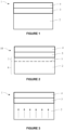
- FD-SOI type substrate represented schematically on the figure 1 under the reference 1, which successively comprises, from its base to its top, a single-crystal semiconductor substrate 2, an electrically insulating layer 3, and a single-crystal semiconductor layer 4.
- the single-crystal substrate 2 is a substrate with high electrical resistivity, and thus has an electrical resistivity of between 500 ⁇ .cm and 30 k ⁇ .cm.
- the single-crystal substrate 2 is a substrate having a high quantity of oxygen, and thus has an interstitial oxygen content (Oi) of between 20 and 40 ppma. Oxygen is trapped in the structure of the monocrystalline substrate, more precisely in the interstices located between the grains of the material constituting the monocrystalline substrate, and is therefore called “interstitial oxygen”.
- the monocrystalline substrate with high electrical resistivity and high quantity of interstitial oxygen is also designated as HR HiOi substrate (combination of the acronyms of the Anglo-Saxon terms “High Resistivity” and “High Oxygen”).
- the single-crystal substrate is made of silicon.
- the single-crystal substrate has P or N type doping.
- the single-crystal substrate 2 is preferably doped with phosphorus, and more preferably, the single-crystal substrate is made of silicon doped with phosphorus.
- the single-crystal substrate 2 is preferably doped with boron, and more preferably, the single-crystal substrate is made of silicon doped with boron.
- the electrically insulating layer 3 comprises a layer of silicon oxide.
- the single crystal layer 3 has P-type doping.
- the single crystal layer is a silicon layer.
- a heat treatment is applied to the FD-SOI type substrate at a temperature greater than or equal to 1175°C, for a time greater than or equal to 1 hour.
- a PN junction, referenced 5, is formed in the monocrystalline substrate 2 at a depth determined with respect to the electrically insulating layer 3, as illustrated in figure 2 .
- heat treatment causes the following phenomena.
- P-type dopants from the single-crystal layer diffuse into the single-crystal substrate through the electrically insulating layer, in a region of the substrate adjacent to the electrically insulating layer.
- the single-crystal substrate is P-type doped
- an inversion of the type of doping occurs in the single-crystal substrate 2.
- the substrate a region 6, called the first region, which extends from the base of the monocrystalline substrate to the P-N junction and which is doped with type N due to the inversion of the type of doping.
- the P-N junction marks the boundary between the first region 6, and the remaining region 7 of the monocrystalline substrate, called the second region, which extends from the P-N junction to the electrically insulating layer 3, and which remains P-type doped. , the diffusion of P-type dopants in this second region having compensated for the inversion of the doping type.
- the single-crystal substrate is N-doped
- the aforementioned phenomenon of diffusion of P-type dopants in the second region occurs.
- the phenomenon of reversal of the type of doping does not occur.
- the first region remains N-type doped.
- the monocrystalline substrate comprises a P-N junction separating the first region (located on the base side of the substrate) doped with type N and the second region ( located on the side of the electrically insulating layer) doped with type P.
- the adjustment of these three characteristics makes it possible to control the formation of the PN junction, and in particular its depth in the monocrystalline substrate 2 from the electrically insulating layer 3.
- the process parameters are adjusted so as to form the P-N junction at a depth of between 1 ⁇ m and 5 ⁇ m from the electrically insulating layer.
- the heat treatment causes the interstitial oxygen present in the monocrystalline substrate 2 to precipitate, which forms thermal donors of the sulfur oxides type S x O y equipped with excess charges coming to dop the material of the monocrystalline substrate, and thus reverse the doping of the latter.
- This first phenomenon is represented schematically on the Figure 3 , on which the doping of the material of the monocrystalline substrate by the thermal donors is represented by the vertical ascending arrows 8.
- the heat treatment causes the diffusion of the dopants of the monocrystalline layer 4, such as boron, through the electrically insulating layer 3 which is sufficiently thin, into the monocrystalline substrate 2.
- dopants can also be used to control the formation of the PN junction, and in particular its depth in the monocrystalline substrate from the electrically insulating layer.
- This second phenomenon is represented schematically on the figure 4 , on which the diffusion of dopants through the electrically insulating layer is represented by the downward vertical arrows 9.
- This second phenomenon combined with the first in the case of a monocrystalline substrate doped with tpe P, leads to the formation of the first region of the N-doping substrate, and to the formation of the second P-doped region, located between the first region and the electrically insulating layer, visible on the semiconductor-on-insulator type structure 10 of the figure 2 .
- the method of the invention offers the advantage of allowing these two phenomena to occur thanks to the three characteristics listed above, without the need for additional processing steps.
- the formation of the P-N junction in the thickness of the substrate in the present invention does not require any localized implantation of dopants or any mask deposition. on the substrate.
- the FD-SOI type substrate is obtained by transferring a layer of a donor substrate to a recipient substrate.
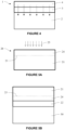
- a donor substrate 20 comprising a single-crystal layer 21, preferably a silicon layer, having P-type doping, and a weakening zone 23 located in the single-crystal layer delimiting the layer to be transferred 24, as illustrated on there figure 5A .
- the single-crystal layer 24 to be transferred is preferably a silicon layer.
- a monocrystalline receiver substrate 30 is also provided, preferably made of silicon, having an electrical resistivity of between 500 ⁇ .cm and 30 k ⁇ .cm, an interstitial oxygen content (Oi) of between 20 and 40 ppma, and a doping of type P or N.
- the donor substrate 20 is then bonded to the recipient substrate 30 via an electrically insulating layer 22 having a thickness of between 20 nm and 400 nm.
- the electrically insulating layer 22 is then located between the donor substrate 20 and the recipient substrate 30.
- the electrically insulating layer 22 can come from the donor substrate or from the recipient substrate, that is to say it can be initially on the donor substrate or on the recipient substrate before bonding.
- the transfer of layer 24 from the donor substrate 20 to the recipient substrate 30 is carried out in accordance with the Smart Cut TM process, in which the weakened zone 23 is formed by implantation of atomic species, such as for example d atoms. hydrogen and/or helium, in the donor substrate, then the donor substrate is detached along said weakening zone.
- the Smart Cut TM process in which the weakened zone 23 is formed by implantation of atomic species, such as for example d atoms. hydrogen and/or helium, in the donor substrate, then the donor substrate is detached along said weakening zone.
- a donor substrate 20 comprising a single-crystal semiconductor layer 21, preferably a silicon layer, having P-type doping.
- the single crystal layer 21 is preferably a silicon layer.
- a monocrystalline receiver substrate 30 is also provided, preferably made of silicon, having an electrical resistivity of between 500 ⁇ .cm and 30 k ⁇ .cm, an interstitial oxygen content (Oi) of between 20 and 40 ppma, and a doping of type P or N.
- the donor substrate 20 is then bonded to the recipient substrate 30 via an electrically insulating layer 22 having a thickness of between 20 nm and 400 nm.
- the electrically insulating layer 22 is then located between the donor substrate 20 and the recipient substrate 30.
- the electrically insulating layer 22 can come from the donor substrate or from the recipient substrate, that is to say it can be initially on the donor substrate or on the recipient substrate before bonding.
- the donor substrate 20 is then thinned from the surface opposite the recipient substrate to form the transferred layer 24, in order to obtain the substrate 1 of the FD-SOI type.
- FIG. 7 is a graph which illustrates the HD2 gain (dBm) for a semiconductor-on-insulator type structure with or without a PN junction in the high electrical resistivity substrate.
- the HD2 gain corresponds to the second harmonic, measured at a frequency of 900 MHz.
- HD2 is the harmonic generated by the substrate which can interfere with the operation of a radio frequency device comprising the structure according to the invention.
- HD2 is measured across a coplanar line with an entry point and an exit point.
- a power P in (dBm) is imposed, and at the output we measure the power P out which is broken down into several harmonics including in particular HD1 which corresponds to the power measured at the output approximately equal to the power of input, and HD2 which corresponds to the harmonic generated by the substrate.
- the HD2 gain obtained for the structure comprising a PN junction (curve C1) is lower than that obtained for a structure without PN junction (curve C2).
- This downward shift of the C2 curve relative to the C1 curve corresponds to a loss of approximately 10 dBm.
- the high resistivity substrate of the P-N junction structure is more electrically insulating than that of the structure without P-N junction.
- FIG. 8 is a graph which illustrates the S21 gain (dB) for a semiconductor-on-insulator type structure with or without a PN junction, as a function of frequency (Hz).
- the gain S21 corresponds to a measurement of crosstalk or noise (called “cross-talk” in English) which reflects the capacity of components compared to others to communicate through the substrate, thus representing the insulation performance of the substrate.
- FIG. 9 is a graph which illustrates the resistivity R (ohm.cm) of a semiconductor-on-insulator type structure with or without a PN junction in the high electrical resistivity substrate, as a function of frequency (Hz).
- the resistivity obtained for the structure including a PN junction is greater than that obtained for a structure without PN junction (curve C6).
- This downward shift of the C5 curve relative to the C6 curve corresponds to a loss of approximately 1200 ohm.cm.
- the graphs of figures 7, 8 , And 9 thus show that the radio frequency performances of the semiconductor-on-insulator type structure of the invention, comprising a PN junction, are greatly improved compared to those of a structure without a PN junction.
Landscapes
- Recrystallisation Techniques (AREA)
- Element Separation (AREA)
- Thin Film Transistor (AREA)
- Crystals, And After-Treatments Of Crystals (AREA)
Claims (8)
- Verfahren zur Herstellung einer Struktur vom Typ Halbleiter auf Isolator (10), das die folgenden Schritte umfasst:- Bereitstellen eines Substrats vom Typ FD-SOI (1), das nacheinander von seiner Basis bis zu seiner Spitze umfasst:• ein monokristallines Halbleitersubstrat (2) mit einem elektrischen Widerstand zwischen 500 Ω.cm und 30 kΩ.cm, einem interstitiellen Sauerstoffgehalt (Oi) zwischen 20 und 40 old ppma und mit einer Dotierung eines ersten Typs P oder N,• eine elektrisch isolierende Schicht (3) mit einer Dicke zwischen 20 nm und 400 nm, und• eine monokristalline halbleitende Schicht (4) mit einer Dotierung vom Typ P,- Wärmebehandlung des Substrats vom Typ FD-SOI (1) bei einer Temperatur über oder gleich 1175 °C während einer Zeit über oder gleich 1 h, um eine P-N-Verbindung (5) im monokristallinen Halbleitersubstrat (2) in einer bestimmten Tiefe in Bezug auf die elektrisch isolierende Schicht (3) zu bilden,um in dem Substrat einen ersten Bereich (6) mit einer Dotierung vom Typ N zu bilden, der sich zwischen der Basis des Substrats und der P-N-Verbindung erstreckt, und einen zweiten P-dotierten Bereich (7), der sich zwischen dem ersten Bereich (6) und der elektrisch isolierenden Schicht (3) befindet.• durch Diffusion von Dotiermitteln des Typs P aus der monokristallinen halbleitenden Schicht (4) durch die elektrisch isolierende Schicht (3) in das Substrat (2),• und, wenn das Substrat (2) eine Dotierung vom Typ P aufweist, durch Bildung thermischer Donoren in dem Substrat (2) durch Ausfällung des interstitiellen Sauerstoffs,
- Herstellungsverfahren nach Anspruch 1, wobei das monokristalline Substrat (2) aus Silizium besteht und/oder die monokristalline Schicht (4) eine Siliziumschicht ist.
- Herstellungsverfahren nach Anspruch 1 oder Anspruch 2, wobei das Substrat vom Typ FD-SOI (1) durch Übertragung einer Schicht (24) eines Donorsubstrats (20) auf ein Aufnahmesubstrat (30) in folgenden Schritten erhalten wird:- Bereitstellung• des Donorsubstrats (20), das eine monokristalline halbleitende Schicht (21) mit einer Dotierung vom Typ P und eine Schwächungszone (23) umfasst, die sich in der monokristallinen Siliziumschicht (21) befindet, die die zu übertragende Schicht (24) begrenzt, und• des monokristallinen halbleitenden Aufnahmesubstrats (30) mit einem elektrischen Widerstand zwischen 500 Ω.cm und 30 kΩ.cm, einem interstitiellen Sauerstoffgehalt (Oi) zwischen 20 und 40 old ppma und einer Dotierung eines ersten Typs P oder N,- Kleben des Donorsubstrats (20) auf das Aufnahmesubstrat (30) über eine elektrisch isolierende Schicht (22), die eine Dicke zwischen 20 nm und 400 nm aufweist,- Ablösen des Donorsubstrats (20) entlang der Schwächungszone (23), um das Substrat vom Typ FD-SOI (1) zu bilden.
- Herstellungsverfahren nach Anspruch 1 oder Anspruch 2, wobei das Substrat vom Typ FD-SOI (1) durch Übertragung einer Schicht (24) eines Donorsubstrats (20) auf ein Aufnahmesubstrat (30) in folgenden Schritten erhalten wird:- Bereitstellung:• des Donorsubstrats (20), das eine monokristalline halbleitende Schicht (21) mit einer Dotierung vom Typ P umfasst, und• des monokristallinen halbleitenden Aufnahmesubstrats (30) mit einem elektrischen Widerstand zwischen 500 Ω.cm und 30 kΩ.cm, einem interstitiellen Sauerstoffgehalt (Oi) zwischen 20 und 40 old ppma und einer Dotierung vom Typ P oder N,- Kleben des Donorsubstrats (20) auf das Aufnahmesubstrat (30) über eine elektrisch isolierende Schicht (22), die eine Dicke zwischen 20 nm und 400 nm aufweist,- Ausdünnen des Donorsubstrats (20) ab der dem Aufnahmesubstrat (30) gegenüberliegenden Oberfläche zur Bildung der übertragenen Schicht (24), um das Substrat vom Typ FD-SOI (1) zu erhalten.
- Verfahren nach Anspruch 3, wobei die Schwächungszone (24) durch Implantation von Atomspezies in das Donorsubstrat (20) gebildet wird, um die zu übertragende Schicht (24) zu begrenzen.
- Verfahren nach einem der Ansprüche 3 bis 5, wobei das Aufnahmesubstrat (30) und die monokristalline Schicht (21) des Donorsubstrats mit Bor P-dotiert sind.
- Verfahren nach einem der vorhergehenden Ansprüche, wobei die P-N-Verbindung (5) in einer Tiefe zwischen 1 µm und 5 µm ab der elektrisch isolierenden Schicht (3) gebildet wird.
- Verfahren nach einem der vorhergehenden Ansprüche, wobei die elektrisch isolierende Schicht (3) eine Siliziumoxidschicht umfasst.
Applications Claiming Priority (2)
| Application Number | Priority Date | Filing Date | Title |
|---|---|---|---|
| FR2000098A FR3106019B1 (fr) | 2020-01-07 | 2020-01-07 | Procede de fabrication d’une structure de type semi-conducteur sur isolant pour applications radiofréquences |
| PCT/FR2021/050018 WO2021140300A1 (fr) | 2020-01-07 | 2021-01-07 | Procede de fabrication d'une structure de type semi-conducteur sur isolant pour applications radiofréquences |
Publications (3)
| Publication Number | Publication Date |
|---|---|
| EP4088312A1 EP4088312A1 (de) | 2022-11-16 |
| EP4088312B1 true EP4088312B1 (de) | 2024-03-13 |
| EP4088312C0 EP4088312C0 (de) | 2024-03-13 |
Family
ID=70154624
Family Applications (1)
| Application Number | Title | Priority Date | Filing Date |
|---|---|---|---|
| EP21704847.9A Active EP4088312B1 (de) | 2020-01-07 | 2021-01-07 | Verfahren zur herstellung einer halbleiter-auf-isolator-struktur für hochfrequenzanwendungen |
Country Status (7)
| Country | Link |
|---|---|
| US (1) | US20230025429A1 (de) |
| EP (1) | EP4088312B1 (de) |
| JP (1) | JP7663582B2 (de) |
| KR (1) | KR102949006B1 (de) |
| CN (1) | CN114930516B (de) |
| FR (1) | FR3106019B1 (de) |
| WO (1) | WO2021140300A1 (de) |
Families Citing this family (1)
| Publication number | Priority date | Publication date | Assignee | Title |
|---|---|---|---|---|
| FR3133481A1 (fr) * | 2022-03-11 | 2023-09-15 | Soitec | Procédé de fabrication d’une structure multicouche de type semi-conducteur sur isolant |
Family Cites Families (14)
| Publication number | Priority date | Publication date | Assignee | Title |
|---|---|---|---|---|
| JP3542376B2 (ja) * | 1994-04-08 | 2004-07-14 | キヤノン株式会社 | 半導体基板の製造方法 |
| JPH11330437A (ja) * | 1998-05-13 | 1999-11-30 | Nec Corp | Soi基板とその製造方法 |
| JP2003224247A (ja) | 2002-01-29 | 2003-08-08 | Shin Etsu Handotai Co Ltd | Soiウエーハ及びsoiウエーハの製造方法 |
| JP5528667B2 (ja) | 2007-11-28 | 2014-06-25 | ルネサスエレクトロニクス株式会社 | 半導体装置および半導体装置の制御方法 |
| JP5625239B2 (ja) | 2008-12-25 | 2014-11-19 | 信越半導体株式会社 | 貼り合わせウェーハの製造方法 |
| WO2012125632A1 (en) * | 2011-03-16 | 2012-09-20 | Memc Electronic Materials, Inc. | Silicon on insulator structures having high resistivity regions in the handle wafer and methods for producing such structures |
| US8536035B2 (en) | 2012-02-01 | 2013-09-17 | International Business Machines Corporation | Silicon-on-insulator substrate and method of forming |
| US9768056B2 (en) | 2013-10-31 | 2017-09-19 | Sunedison Semiconductor Limited (Uen201334164H) | Method of manufacturing high resistivity SOI wafers with charge trapping layers based on terminated Si deposition |
| KR102360695B1 (ko) | 2014-01-23 | 2022-02-08 | 글로벌웨이퍼스 씨오., 엘티디. | 고 비저항 soi 웨이퍼 및 그 제조 방법 |
| JP6749394B2 (ja) * | 2015-11-20 | 2020-09-02 | グローバルウェーハズ カンパニー リミテッドGlobalWafers Co.,Ltd. | 滑らかな半導体表面の製造方法 |
| US9613805B1 (en) * | 2015-12-11 | 2017-04-04 | Infineon Technologies Ag | Method for forming a semiconductor device |
| FR3051968B1 (fr) | 2016-05-25 | 2018-06-01 | Soitec | Procede de fabrication d'un substrat semi-conducteur a haute resistivite |
| US10269617B2 (en) | 2016-06-22 | 2019-04-23 | Globalwafers Co., Ltd. | High resistivity silicon-on-insulator substrate comprising an isolation region |
| FR3058561B1 (fr) | 2016-11-04 | 2018-11-02 | Soitec | Procede de fabrication d'un element semi-conducteur comprenant un substrat hautement resistif |
-
2020
- 2020-01-07 FR FR2000098A patent/FR3106019B1/fr active Active
-
2021
- 2021-01-07 US US17/757,822 patent/US20230025429A1/en active Pending
- 2021-01-07 CN CN202180008062.5A patent/CN114930516B/zh active Active
- 2021-01-07 JP JP2022538205A patent/JP7663582B2/ja active Active
- 2021-01-07 KR KR1020227025992A patent/KR102949006B1/ko active Active
- 2021-01-07 WO PCT/FR2021/050018 patent/WO2021140300A1/fr not_active Ceased
- 2021-01-07 EP EP21704847.9A patent/EP4088312B1/de active Active
Also Published As
| Publication number | Publication date |
|---|---|
| WO2021140300A1 (fr) | 2021-07-15 |
| KR20220123671A (ko) | 2022-09-08 |
| FR3106019A1 (fr) | 2021-07-09 |
| US20230025429A1 (en) | 2023-01-26 |
| JP2023509380A (ja) | 2023-03-08 |
| EP4088312C0 (de) | 2024-03-13 |
| CN114930516A (zh) | 2022-08-19 |
| JP7663582B2 (ja) | 2025-04-16 |
| KR102949006B1 (ko) | 2026-04-06 |
| EP4088312A1 (de) | 2022-11-16 |
| FR3106019B1 (fr) | 2021-12-10 |
| CN114930516B (zh) | 2025-07-29 |
Similar Documents
| Publication | Publication Date | Title |
|---|---|---|
| EP2279520B1 (de) | Verfahren zur herstellung komplementärer p- und n-mosfet-transistoren | |
| EP3531444B1 (de) | Integrierter schaltkreis, der ein substrat mit einem bereich mit vielen haftstellen umfasst, und herstellungsverfahren | |
| FR2616590A1 (fr) | Procede de fabrication d'une couche d'isolant enterree dans un substrat semi-conducteur par implantation ionique et structure semi-conductrice comportant cette couche | |
| EP4030467B1 (de) | Verfahren zum direkten hydrophilen bonden von substraten | |
| EP1949430A1 (de) | Behandlung einer an ein substrat gebondeten germaniumschicht | |
| FR3051596A1 (fr) | Procede de fabrication d'un substrat de type semi-conducteur contraint sur isolant | |
| FR2972567A1 (fr) | Méthode de formation d'une structure de ge sur iii/v sur isolant | |
| EP3127142A1 (de) | Verfahren zur herstellung eines halbleiterwafers zur herstellung eines soi-substrats und damit hergestellter soi-substratwafer | |
| FR3051595A1 (fr) | Procede de fabrication d'un substrat de type semi-conducteur contraint sur isolant | |
| EP0797252B1 (de) | Silizium auf Isolator-Substrat zum Herstellen von Transistoren und Verfahren zum Vorbereiten eines derartigen Substrats | |
| EP4088312B1 (de) | Verfahren zur herstellung einer halbleiter-auf-isolator-struktur für hochfrequenzanwendungen | |
| FR2693314A1 (fr) | Transistor JFET vertical à mode de fonctionnement bipolaire optimisé et procédé de fabrication correspondant. | |
| WO2022195226A1 (fr) | Transistor nc-fet comportant un substrat du type semi-conducteur sur isolant | |
| EP3903342B1 (de) | Halbleiterstruktur für digitale und hochfrequente anwendungen und verfahren zur herstellung einer solchen struktur | |
| EP3903340B1 (de) | Halbleiterstruktur für digitale und hochfrequente anwendungen | |
| FR3136109A1 (fr) | Dispositif semiconducteur du type silicium sur isolant et procédé de fabrication correspondant | |
| WO2021234277A1 (fr) | Procede de fabrication d'un substrat semi-conducteur sur isolant pour applications radiofrequences | |
| EP3903341B1 (de) | Verfahren zur herstellung eines substrats für einen vorderseitigen bildsensor | |
| FR3109017A1 (fr) | PROCÉDÉ DE FABRICATION D’UNE PUCE À CIRCUIT INTÉGRÉ sur SeOI | |
| FR3076397A1 (fr) | Procede de fabrication d'un transistor | |
| FR2693313A1 (fr) | Transistor JFET vertical à capacité grille/substrat réduite, et procédé de fabrication correspondant. |
Legal Events
| Date | Code | Title | Description |
|---|---|---|---|
| STAA | Information on the status of an ep patent application or granted ep patent |
Free format text: STATUS: UNKNOWN |
|
| STAA | Information on the status of an ep patent application or granted ep patent |
Free format text: STATUS: THE INTERNATIONAL PUBLICATION HAS BEEN MADE |
|
| PUAI | Public reference made under article 153(3) epc to a published international application that has entered the european phase |
Free format text: ORIGINAL CODE: 0009012 |
|
| STAA | Information on the status of an ep patent application or granted ep patent |
Free format text: STATUS: REQUEST FOR EXAMINATION WAS MADE |
|
| 17P | Request for examination filed |
Effective date: 20220722 |
|
| AK | Designated contracting states |
Kind code of ref document: A1 Designated state(s): AL AT BE BG CH CY CZ DE DK EE ES FI FR GB GR HR HU IE IS IT LI LT LU LV MC MK MT NL NO PL PT RO RS SE SI SK SM TR |
|
| DAV | Request for validation of the european patent (deleted) | ||
| DAX | Request for extension of the european patent (deleted) | ||
| STAA | Information on the status of an ep patent application or granted ep patent |
Free format text: STATUS: EXAMINATION IS IN PROGRESS |
|
| 17Q | First examination report despatched |
Effective date: 20230629 |
|
| REG | Reference to a national code |
Ref legal event code: R079 Ref country code: DE Ref legal event code: R079 Ref document number: 602021010401 Country of ref document: DE Free format text: PREVIOUS MAIN CLASS: H01L0021761000 Ipc: H01L0021324000 |
|
| GRAP | Despatch of communication of intention to grant a patent |
Free format text: ORIGINAL CODE: EPIDOSNIGR1 |
|
| STAA | Information on the status of an ep patent application or granted ep patent |
Free format text: STATUS: GRANT OF PATENT IS INTENDED |
|
| RIC1 | Information provided on ipc code assigned before grant |
Ipc: H01L 21/761 20060101ALI20231121BHEP Ipc: H01L 21/02 20060101ALI20231121BHEP Ipc: H01L 21/762 20060101ALI20231121BHEP Ipc: H01L 21/225 20060101ALI20231121BHEP Ipc: H01L 21/324 20060101AFI20231121BHEP |
|
| INTG | Intention to grant announced |
Effective date: 20231207 |
|
| GRAS | Grant fee paid |
Free format text: ORIGINAL CODE: EPIDOSNIGR3 |
|
| GRAA | (expected) grant |
Free format text: ORIGINAL CODE: 0009210 |
|
| STAA | Information on the status of an ep patent application or granted ep patent |
Free format text: STATUS: THE PATENT HAS BEEN GRANTED |
|
| AK | Designated contracting states |
Kind code of ref document: B1 Designated state(s): AL AT BE BG CH CY CZ DE DK EE ES FI FR GB GR HR HU IE IS IT LI LT LU LV MC MK MT NL NO PL PT RO RS SE SI SK SM TR |
|
| REG | Reference to a national code |
Ref country code: GB Ref legal event code: FG4D Free format text: NOT ENGLISH |
|
| REG | Reference to a national code |
Ref country code: CH Ref legal event code: EP |
|
| REG | Reference to a national code |
Ref country code: DE Ref legal event code: R096 Ref document number: 602021010401 Country of ref document: DE |
|
| REG | Reference to a national code |
Ref country code: IE Ref legal event code: FG4D Free format text: LANGUAGE OF EP DOCUMENT: FRENCH |
|
| U01 | Request for unitary effect filed |
Effective date: 20240405 |
|
| U07 | Unitary effect registered |
Designated state(s): AT BE BG DE DK EE FI FR IT LT LU LV MT NL PT SE SI Effective date: 20240415 |
|
| PG25 | Lapsed in a contracting state [announced via postgrant information from national office to epo] |
Ref country code: GR Free format text: LAPSE BECAUSE OF FAILURE TO SUBMIT A TRANSLATION OF THE DESCRIPTION OR TO PAY THE FEE WITHIN THE PRESCRIBED TIME-LIMIT Effective date: 20240614 |
|
| PG25 | Lapsed in a contracting state [announced via postgrant information from national office to epo] |
Ref country code: HR Free format text: LAPSE BECAUSE OF FAILURE TO SUBMIT A TRANSLATION OF THE DESCRIPTION OR TO PAY THE FEE WITHIN THE PRESCRIBED TIME-LIMIT Effective date: 20240313 Ref country code: RS Free format text: LAPSE BECAUSE OF FAILURE TO SUBMIT A TRANSLATION OF THE DESCRIPTION OR TO PAY THE FEE WITHIN THE PRESCRIBED TIME-LIMIT Effective date: 20240613 |
|
| PG25 | Lapsed in a contracting state [announced via postgrant information from national office to epo] |
Ref country code: ES Free format text: LAPSE BECAUSE OF FAILURE TO SUBMIT A TRANSLATION OF THE DESCRIPTION OR TO PAY THE FEE WITHIN THE PRESCRIBED TIME-LIMIT Effective date: 20240313 |
|
| PG25 | Lapsed in a contracting state [announced via postgrant information from national office to epo] |
Ref country code: RS Free format text: LAPSE BECAUSE OF FAILURE TO SUBMIT A TRANSLATION OF THE DESCRIPTION OR TO PAY THE FEE WITHIN THE PRESCRIBED TIME-LIMIT Effective date: 20240613 Ref country code: NO Free format text: LAPSE BECAUSE OF FAILURE TO SUBMIT A TRANSLATION OF THE DESCRIPTION OR TO PAY THE FEE WITHIN THE PRESCRIBED TIME-LIMIT Effective date: 20240613 Ref country code: HR Free format text: LAPSE BECAUSE OF FAILURE TO SUBMIT A TRANSLATION OF THE DESCRIPTION OR TO PAY THE FEE WITHIN THE PRESCRIBED TIME-LIMIT Effective date: 20240313 Ref country code: GR Free format text: LAPSE BECAUSE OF FAILURE TO SUBMIT A TRANSLATION OF THE DESCRIPTION OR TO PAY THE FEE WITHIN THE PRESCRIBED TIME-LIMIT Effective date: 20240614 Ref country code: ES Free format text: LAPSE BECAUSE OF FAILURE TO SUBMIT A TRANSLATION OF THE DESCRIPTION OR TO PAY THE FEE WITHIN THE PRESCRIBED TIME-LIMIT Effective date: 20240313 |
|
| PG25 | Lapsed in a contracting state [announced via postgrant information from national office to epo] |
Ref country code: IS Free format text: LAPSE BECAUSE OF FAILURE TO SUBMIT A TRANSLATION OF THE DESCRIPTION OR TO PAY THE FEE WITHIN THE PRESCRIBED TIME-LIMIT Effective date: 20240713 |
|
| PG25 | Lapsed in a contracting state [announced via postgrant information from national office to epo] |
Ref country code: SM Free format text: LAPSE BECAUSE OF FAILURE TO SUBMIT A TRANSLATION OF THE DESCRIPTION OR TO PAY THE FEE WITHIN THE PRESCRIBED TIME-LIMIT Effective date: 20240313 |
|
| PG25 | Lapsed in a contracting state [announced via postgrant information from national office to epo] |
Ref country code: CZ Free format text: LAPSE BECAUSE OF FAILURE TO SUBMIT A TRANSLATION OF THE DESCRIPTION OR TO PAY THE FEE WITHIN THE PRESCRIBED TIME-LIMIT Effective date: 20240313 |
|
| PG25 | Lapsed in a contracting state [announced via postgrant information from national office to epo] |
Ref country code: PL Free format text: LAPSE BECAUSE OF FAILURE TO SUBMIT A TRANSLATION OF THE DESCRIPTION OR TO PAY THE FEE WITHIN THE PRESCRIBED TIME-LIMIT Effective date: 20240313 |
|
| PG25 | Lapsed in a contracting state [announced via postgrant information from national office to epo] |
Ref country code: SK Free format text: LAPSE BECAUSE OF FAILURE TO SUBMIT A TRANSLATION OF THE DESCRIPTION OR TO PAY THE FEE WITHIN THE PRESCRIBED TIME-LIMIT Effective date: 20240313 |
|
| PG25 | Lapsed in a contracting state [announced via postgrant information from national office to epo] |
Ref country code: SM Free format text: LAPSE BECAUSE OF FAILURE TO SUBMIT A TRANSLATION OF THE DESCRIPTION OR TO PAY THE FEE WITHIN THE PRESCRIBED TIME-LIMIT Effective date: 20240313 Ref country code: SK Free format text: LAPSE BECAUSE OF FAILURE TO SUBMIT A TRANSLATION OF THE DESCRIPTION OR TO PAY THE FEE WITHIN THE PRESCRIBED TIME-LIMIT Effective date: 20240313 Ref country code: RO Free format text: LAPSE BECAUSE OF FAILURE TO SUBMIT A TRANSLATION OF THE DESCRIPTION OR TO PAY THE FEE WITHIN THE PRESCRIBED TIME-LIMIT Effective date: 20240313 Ref country code: PL Free format text: LAPSE BECAUSE OF FAILURE TO SUBMIT A TRANSLATION OF THE DESCRIPTION OR TO PAY THE FEE WITHIN THE PRESCRIBED TIME-LIMIT Effective date: 20240313 Ref country code: IS Free format text: LAPSE BECAUSE OF FAILURE TO SUBMIT A TRANSLATION OF THE DESCRIPTION OR TO PAY THE FEE WITHIN THE PRESCRIBED TIME-LIMIT Effective date: 20240713 Ref country code: CZ Free format text: LAPSE BECAUSE OF FAILURE TO SUBMIT A TRANSLATION OF THE DESCRIPTION OR TO PAY THE FEE WITHIN THE PRESCRIBED TIME-LIMIT Effective date: 20240313 |
|
| REG | Reference to a national code |
Ref country code: DE Ref legal event code: R097 Ref document number: 602021010401 Country of ref document: DE |
|
| U20 | Renewal fee for the european patent with unitary effect paid |
Year of fee payment: 5 Effective date: 20241205 |
|
| PLBE | No opposition filed within time limit |
Free format text: ORIGINAL CODE: 0009261 |
|
| STAA | Information on the status of an ep patent application or granted ep patent |
Free format text: STATUS: NO OPPOSITION FILED WITHIN TIME LIMIT |
|
| 26N | No opposition filed |
Effective date: 20241216 |
|
| REG | Reference to a national code |
Ref country code: CH Ref legal event code: PL |
|
| PG25 | Lapsed in a contracting state [announced via postgrant information from national office to epo] |
Ref country code: MC Free format text: LAPSE BECAUSE OF FAILURE TO SUBMIT A TRANSLATION OF THE DESCRIPTION OR TO PAY THE FEE WITHIN THE PRESCRIBED TIME-LIMIT Effective date: 20240313 |
|
| GBPC | Gb: european patent ceased through non-payment of renewal fee |
Effective date: 20250107 |
|
| PG25 | Lapsed in a contracting state [announced via postgrant information from national office to epo] |
Ref country code: GB Free format text: LAPSE BECAUSE OF NON-PAYMENT OF DUE FEES Effective date: 20250107 |
|
| PG25 | Lapsed in a contracting state [announced via postgrant information from national office to epo] |
Ref country code: CH Free format text: LAPSE BECAUSE OF NON-PAYMENT OF DUE FEES Effective date: 20250131 |
|
| U20 | Renewal fee for the european patent with unitary effect paid |
Year of fee payment: 6 Effective date: 20251205 |
|
| PG25 | Lapsed in a contracting state [announced via postgrant information from national office to epo] |
Ref country code: IE Free format text: LAPSE BECAUSE OF NON-PAYMENT OF DUE FEES Effective date: 20250107 |