EP4090993B1 - Kohärentes lidar-abbildungssystem - Google Patents
Kohärentes lidar-abbildungssystem Download PDFInfo
- Publication number
- EP4090993B1 EP4090993B1 EP21700308.6A EP21700308A EP4090993B1 EP 4090993 B1 EP4090993 B1 EP 4090993B1 EP 21700308 A EP21700308 A EP 21700308A EP 4090993 B1 EP4090993 B1 EP 4090993B1
- Authority
- EP
- European Patent Office
- Prior art keywords
- optical
- scene
- ref
- imaging system
- pixel
- Prior art date
- Legal status (The legal status is an assumption and is not a legal conclusion. Google has not performed a legal analysis and makes no representation as to the accuracy of the status listed.)
- Active
Links
Images





Classifications
-
- G—PHYSICS
- G01—MEASURING; TESTING
- G01S—RADIO DIRECTION-FINDING; RADIO NAVIGATION; DETERMINING DISTANCE OR VELOCITY BY USE OF RADIO WAVES; LOCATING OR PRESENCE-DETECTING BY USE OF THE REFLECTION OR RERADIATION OF RADIO WAVES; ANALOGOUS ARRANGEMENTS USING OTHER WAVES
- G01S17/00—Systems using the reflection or reradiation of electromagnetic waves other than radio waves, e.g. lidar systems
- G01S17/88—Lidar systems specially adapted for specific applications
- G01S17/89—Lidar systems specially adapted for specific applications for mapping or imaging
-
- G—PHYSICS
- G01—MEASURING; TESTING
- G01S—RADIO DIRECTION-FINDING; RADIO NAVIGATION; DETERMINING DISTANCE OR VELOCITY BY USE OF RADIO WAVES; LOCATING OR PRESENCE-DETECTING BY USE OF THE REFLECTION OR RERADIATION OF RADIO WAVES; ANALOGOUS ARRANGEMENTS USING OTHER WAVES
- G01S17/00—Systems using the reflection or reradiation of electromagnetic waves other than radio waves, e.g. lidar systems
- G01S17/02—Systems using the reflection of electromagnetic waves other than radio waves
- G01S17/06—Systems determining position data of a target
- G01S17/08—Systems determining position data of a target for measuring distance only
- G01S17/32—Systems determining position data of a target for measuring distance only using transmission of continuous waves, whether amplitude-, frequency-, or phase-modulated, or unmodulated
- G01S17/34—Systems determining position data of a target for measuring distance only using transmission of continuous waves, whether amplitude-, frequency-, or phase-modulated, or unmodulated using transmission of continuous, frequency-modulated waves while heterodyning the received signal, or a signal derived therefrom, with a locally-generated signal related to the contemporaneously transmitted signal
-
- G—PHYSICS
- G01—MEASURING; TESTING
- G01S—RADIO DIRECTION-FINDING; RADIO NAVIGATION; DETERMINING DISTANCE OR VELOCITY BY USE OF RADIO WAVES; LOCATING OR PRESENCE-DETECTING BY USE OF THE REFLECTION OR RERADIATION OF RADIO WAVES; ANALOGOUS ARRANGEMENTS USING OTHER WAVES
- G01S17/00—Systems using the reflection or reradiation of electromagnetic waves other than radio waves, e.g. lidar systems
- G01S17/88—Lidar systems specially adapted for specific applications
- G01S17/89—Lidar systems specially adapted for specific applications for mapping or imaging
- G01S17/894—Three-dimensional [3D] imaging with simultaneous measurement of time-of-flight at a two-dimensional [2D] array of receiver pixels, e.g. time-of-flight cameras or flash lidar
-
- G—PHYSICS
- G01—MEASURING; TESTING
- G01S—RADIO DIRECTION-FINDING; RADIO NAVIGATION; DETERMINING DISTANCE OR VELOCITY BY USE OF RADIO WAVES; LOCATING OR PRESENCE-DETECTING BY USE OF THE REFLECTION OR RERADIATION OF RADIO WAVES; ANALOGOUS ARRANGEMENTS USING OTHER WAVES
- G01S7/00—Details of systems according to groups G01S13/00, G01S15/00, G01S17/00
- G01S7/48—Details of systems according to groups G01S13/00, G01S15/00, G01S17/00 of systems according to group G01S17/00
- G01S7/481—Constructional features, e.g. arrangements of optical elements
- G01S7/4811—Constructional features, e.g. arrangements of optical elements common to transmitter and receiver
-
- G—PHYSICS
- G01—MEASURING; TESTING
- G01S—RADIO DIRECTION-FINDING; RADIO NAVIGATION; DETERMINING DISTANCE OR VELOCITY BY USE OF RADIO WAVES; LOCATING OR PRESENCE-DETECTING BY USE OF THE REFLECTION OR RERADIATION OF RADIO WAVES; ANALOGOUS ARRANGEMENTS USING OTHER WAVES
- G01S7/00—Details of systems according to groups G01S13/00, G01S15/00, G01S17/00
- G01S7/48—Details of systems according to groups G01S13/00, G01S15/00, G01S17/00 of systems according to group G01S17/00
- G01S7/481—Constructional features, e.g. arrangements of optical elements
- G01S7/4814—Constructional features, e.g. arrangements of optical elements of transmitters alone
-
- G—PHYSICS
- G01—MEASURING; TESTING
- G01S—RADIO DIRECTION-FINDING; RADIO NAVIGATION; DETERMINING DISTANCE OR VELOCITY BY USE OF RADIO WAVES; LOCATING OR PRESENCE-DETECTING BY USE OF THE REFLECTION OR RERADIATION OF RADIO WAVES; ANALOGOUS ARRANGEMENTS USING OTHER WAVES
- G01S7/00—Details of systems according to groups G01S13/00, G01S15/00, G01S17/00
- G01S7/48—Details of systems according to groups G01S13/00, G01S15/00, G01S17/00 of systems according to group G01S17/00
- G01S7/481—Constructional features, e.g. arrangements of optical elements
- G01S7/4816—Constructional features, e.g. arrangements of optical elements of receivers alone
-
- G—PHYSICS
- G01—MEASURING; TESTING
- G01S—RADIO DIRECTION-FINDING; RADIO NAVIGATION; DETERMINING DISTANCE OR VELOCITY BY USE OF RADIO WAVES; LOCATING OR PRESENCE-DETECTING BY USE OF THE REFLECTION OR RERADIATION OF RADIO WAVES; ANALOGOUS ARRANGEMENTS USING OTHER WAVES
- G01S7/00—Details of systems according to groups G01S13/00, G01S15/00, G01S17/00
- G01S7/48—Details of systems according to groups G01S13/00, G01S15/00, G01S17/00 of systems according to group G01S17/00
- G01S7/481—Constructional features, e.g. arrangements of optical elements
- G01S7/4818—Constructional features, e.g. arrangements of optical elements using optical fibres
-
- G—PHYSICS
- G01—MEASURING; TESTING
- G01S—RADIO DIRECTION-FINDING; RADIO NAVIGATION; DETERMINING DISTANCE OR VELOCITY BY USE OF RADIO WAVES; LOCATING OR PRESENCE-DETECTING BY USE OF THE REFLECTION OR RERADIATION OF RADIO WAVES; ANALOGOUS ARRANGEMENTS USING OTHER WAVES
- G01S7/00—Details of systems according to groups G01S13/00, G01S15/00, G01S17/00
- G01S7/48—Details of systems according to groups G01S13/00, G01S15/00, G01S17/00 of systems according to group G01S17/00
- G01S7/491—Details of non-pulse systems
- G01S7/4912—Receivers
- G01S7/4917—Receivers superposing optical signals in a photodetector, e.g. optical heterodyne detection
-
- G—PHYSICS
- G02—OPTICS
- G02B—OPTICAL ELEMENTS, SYSTEMS OR APPARATUS
- G02B6/00—Light guides; Structural details of arrangements comprising light guides and other optical elements, e.g. couplings
- G02B6/24—Coupling light guides
- G02B6/26—Optical coupling means
- G02B6/34—Optical coupling means utilising prism or grating
Definitions
- the present invention relates to the field of imaging a scene to be observed by a coherent LIDAR and more particularly in the field of three-dimensional imaging by coherent lidar with heterodyne detection.
- Imaging a scene by LIDAR ( Light Detection and Ranging ) with heterodyne detection takes advantage of the nature of the coherent emission of a laser source in order to amplify the useful signal reflected by the scene by a signal from a reference channel and coherent with the useful signal.
- the optical frequency of the laser source is modulated, for example with a periodic linear ramp.
- the light from the laser source is divided into two paths. Part of the light (object path) is projected onto a point in the scene where it is backscattered, partially towards a photodetector. The other part (reference path) is sent to the photodetector without passing through the scene.
- the two paths interfere on the photodetector and form a heterodyne signal.
- the interference produces beats whose frequency is proportional to the delay between the two paths, and therefore to the distance between the scene and the photodetector.
- N N ⁇ T ⁇ f R
- the distance resolution is ⁇ z ⁇ c 2 B .
- the FMCW type LIDAR technique is an optical heterodyne measurement technique since it involves several optical frequencies.
- the heterodyne signal (i.e. interference signal) contains a generally large and useless DC component, which is removed by a high-pass electronic filter if the photoreceiver is a photodiode.
- a 3dB coupler which provides, from the two input object and reference channels, two output signals in phase opposition which illuminate two photodiodes in series (balanced photodiodes).
- the detection circuit makes it possible to differentiate the two photocurrents, thus eliminating the DC (mode common) and detect the AC part.
- the AC part is usually amplified externally by a trans-impedance amplifier (TIA) before being processed by external electronics, for example an oscilloscope, to measure the beat frequency f R . Once the measurement is made, the point is changed, i.e. a sequential spatial scan of the scene is carried out.
- TIA trans-impedance amplifier
- This technique is efficient because the reference channel does not suffer from significant backscattering losses, and is used to amplify the received signal using interferometric mixing that multiplies the amplitude of the useful signal.
- the image obtained is in principle of the " rolling shutter " type, i.e. the pixels are read sequentially, since it is necessary to scan the scene to produce a complete image of it. This technique is therefore disrupted by image distortion when the scene contains moving objects.
- a sequential scanning FMCW type LIDAR imaging system is difficult to match with video rate use (typically 50Hz or 20ms per image).
- video rate use typically 50Hz or 20ms per image.
- a QVGA format image 320 ⁇ 240 or approximately 76800 pixels
- it is necessary to change points every 260ns and therefore make at least one ramp in T 260ns, which requires a laser modulation frequency of several MHz, and even several tens of MHz with linear ramps.
- These values are at the limit of the capabilities of a semiconductor laser by modulation of its current, and beyond the range of a laser tunable by mechanical or thermal means.
- each Res array sends the coupled light to a side-coupled PD photodiode located outside the image, via a waveguide.
- the reference path is directly sent to the photodiodes by an optical fiber Fib and by a network of waveguides and Y junctions.
- the conversion of the photocurrent into voltage is performed by a trans-impedance amplifier TIA for each of the 16 photodiodes.
- Electronic filtering and signal processing are performed outside the chip in an SED electronic detection system. FMCW detection provides access to the distance at each point of the image.
- this coherent LIDAR imager configuration is not easily scalable to a large number of pixels. Indeed, 2N waveguides (N for the reference channel and N for the object channel) would be required for N pixels, i.e. 2 million waveguides for a 1000 ⁇ 1000 pixel imager, which poses significant routing and surface area problems. To artificially increase the effective number of pixels of their imager, the authors use the technique of multiple shots with successive mechanical translations of the imager, which is not suitable for moving scenes.
- the proposed architecture is sensitive to speckle grains generated by the scattering of coherent light by the scene (the image of the object in the sensor plane is tainted by speckle grains, i.e. laser granularity).
- speckle grains i.e. laser granularity.
- the beats due to the interference between the reference channel and the object channel affected by the speckle grains are of the same frequency but randomly shifted between neighboring speckle grains. If the pixels are larger than the speckle grains, the amplitude of the resulting oscillations is attenuated and may become undetectable. Note that, in the configuration of Aflatouni et al.
- an aperture number (f # ) of at least 6 would be required to have speckle grains larger than the pixels.
- a narrow aperture optic is not favorable for the detection of objects that are not very reflective or located at significant distances and, in return, requires the use of a more powerful laser source.
- the document WO 2019/041274 A1 relates to a LIDAR imaging system, and describes in particular an optical device for shaping the transmitted beam.
- the document US 2017/118423 A1 relates to an imaging system for reducing glare from a diffusing medium (e.g. fog).
- the article by Amann et al. entitled Laser ranging: a critical review of usual techniques for distance measurement Opt. Eng. 40(1) 10-19 (January 2001 ) covers laser distance measurement techniques, including the FMCW technique. In particular, it describes a method for calculating the distance from the measured beat frequency.
- the document US 2018/232048 A1 describes a waveguide comprising a diffraction grating.
- the document US 5,610,705 A deals with heterodyne detection by laser velocimetry. In particular, it describes a method for making the wavefront of a reference beam close to that of the reflected beam.
- the invention aims to remedy at least in part certain drawbacks of the prior art, and more precisely to propose a coherent LIDAR imaging system whose performances are improved. These performances can result in a better quality of the recombined beam (heterodyne signal) detected by the pixels of the detector, for example in terms of intensity of the heterodyne signal.
- the imaging system according to the invention comprises a matrix of pixels at which the scene, illuminated simultaneously, is imaged. Furthermore, each pixel of the detector can comprise an electronic circuit adapted to determine the frequency of the beat of the recombined beam (heterodyne signal) detected.
- FIG 2 represents a schematic view of a coherent LIDAR imaging system D according to an embodiment of the invention.
- the imaging system D makes it possible to acquire an instantaneous distance image of a scene to be illuminated/observed Obj by performing an interference of an object path (object beam reflected L or by the scene) with a reference path (reference beam L ref ) on a pixel matrix using an optical imaging device Im producing an image of the scene.
- the imaging system D is called “LIDAR” (acronym for Light Detection and Ranging ) insofar as it is adapted to provide a mapping of the distance (or distance image) of a scene illuminated by a coherent optical signal.
- the imaging system illuminates the entire scene instantaneously by a continuous optical signal, and simultaneously acquires the image of the illuminated scene to determine the distance.
- the imaging system according to the invention is thus distinguished from LIDAR systems (of the time-of-flight measurement type (TOF, for Time Of Flight, in English) or even of the FMCW type), in which the scene is “scanned”, i.e. spatially scanned by an optical signal.
- the imaging system D is said to have heterodyne detection insofar as, to determine the distance of the illuminated scene, a so-called beat frequency of a heterodyne signal (recombined beam) formed by the interference between a reference beam of a local oscillator and a beam backscattered/reflected by the illuminated scene is determined, these two optical beams being coherent with each other.
- the reference beam and the beam projected onto the scene are in fact both from the same primary optical signal (laser radiation L) emitted by the laser source.
- Heterodyne detection is of the FMCW type insofar as the primary signal is a continuous and frequency modulated signal.
- the imager can be of the global shutter type where all the pixels P i are read at the same time.
- the imaging system can then provide an instantaneous distance image.
- it can be of the rolling shutter type, and therefore have a sequential reading of the pixels P i , for example line by line, where all the pixels P i of the same line are read simultaneously.
- the imaging system D comprises a laser source SL configured to emit laser radiation L having a temporally modulated optical frequency F L.
- the laser source is configured so that a coherence length of the source is twice as large, preferably 10 times as large, as a maximum predetermined distance z max between the most distant object of the scene and the imaging system D.
- the imaging system D being a coherent LIDAR
- the coherence length I c of the laser source is greater than the optical path difference between the object path and the reference path - which is approximately the round-trip distance between the scene to be observed Obj and the imaging system D, (minus the optical path of the reference beam between the splitter plate and the recombination plate) - in order to achieve coherent detection.
- the reference path is the path followed by the reference beam L ref between the laser source SL and the matrix detector Det.
- the object path is the forward path followed by the object beam L o from the laser source SL to the scene, plus the return path followed by the reflected/backscattered object beam L or by the scene to the matrix detector Det.
- the laser radiation L emitted by the laser source SL is a primary, coherent, continuous and frequency-modulated signal. It is frequency-modulated, for example here linearly, from a starting frequency f 0 over a repetition period T with a bandwidth B.
- the signal here is a chirped signal, i.e. a sinusoidal wave whose instantaneous frequency evolves linearly over time.
- the SL laser source can be, in the case of an emission in the near infrared range (between 0.7 and 2 ⁇ m), of the vertical cavity surface emitting laser (VCSEL) type, which generally has a coherence length of the order of a meter, or even of the edge emitting laser (EEL) type, which can have a coherence length of the order of tens or even hundreds of meters.
- VCSEL vertical cavity surface emitting laser
- EEL edge emitting laser
- Passive optical elements may be located on the optical path of the laser radiation L (primary signal), between the laser source SL and the optical separation/recombination device SSR.
- a shaping lens may be located at the output of the laser source SL, and makes it possible to collimate the optical beam while widening its lateral dimension, for example to a diameter of a few millimeters.
- a spatial filtering device may be present to suppress high spatial frequencies.
- the laser radiation L can propagate in a collimated manner, with a possibly Gaussian profile and a diameter of the order of a few millimeters, for example 5 mm.
- the optical separation device is configured so that the distribution of the intensity of the light radiation of the reference beam L ref and the object beam L o is approximately equal to 10%/90% (at the output of the optical separation device LS).
- Other intensity ratio values may be chosen to optimize the photometric performance of the imaging system D, in particular according to the characteristics of the scene (for example, Lambertian or specular reflection) and of the imaging system D (for example the separation and recombination factors of the optical separation and recombination device).
- the imaging system D is therefore adapted to project a portion of the laser radiation L towards a scene which is to be illuminated instantaneously.
- scene is meant the scene illuminated by the object beam L o .
- the entire scene is illuminated instantaneously by the object beam L o , which therefore has an angular aperture capable of illuminating the entire scene instantaneously.
- the scene is furthermore illuminated uniformly, i.e. the object beam L o has an intensity whose angular distribution is constant.
- the imaging system D can ensure shaping of the object beam L o .
- it can include at least at least one optical element adapted to make the object beam L o divergent.
- the angular aperture of the object beam L o is such that the entire scene is uniformly illuminated by the object beam L o . It is preferably substantially equal to the field angle of the optical imaging device Im (for example equal to approximately 20°).
- it may comprise at least one optical element adapted to make the angular distribution of the intensity constant, to obtain a flat intensity profile, and no longer a Gaussian profile.
- the different optical elements may be distinct or merged.
- the imaging system D further comprises an optical imaging device Im adapted to perform the imaging of the scene to be observed Obj on a detector Det by focusing the reflected object beam L o,r .
- the detector Det is placed approximately in the image focal plane of the optical imaging device lm.
- the optical imaging device Im has a focal length much smaller than the typical distance between the scene and the detector Det, so that the scene is considered at infinity from the point of view of the optical imaging device lm.
- the optical imaging device Im is an objective comprising an aperture diaphragm Diaph defining the physical pupil of the system.
- the optical imaging device Im allows the use of a common channel to produce an image of the scene and to interfere the object channel and the reference channel. This allows a greater compactness of the imaging system D compared to prior art lidars using waveguide recombination.
- the imaging optical device Im has free-space optical elements, and comprises at least one lens and an aperture diaphragm that defines the physical pupil.
- the aperture diaphragm may not be a physical object distinct from a lens, but may be defined by the outline of the lens.
- the imaging optical device Im comprises an optical axis AO orthogonal to the reception plane of the matrix detector Det. It is here adapted to receive the reflected object beam L or as well as the reference beam L ref , to allow their transmission towards the matrix detector Det along the same optical axis AO and thus allow a better superposition of the two optical beams, thus improving the combination of the two optical beams by interference, which makes it possible to improve the intensity of the heterodyne signal.
- the optical imaging device Im is formed of a lens or a plurality of lenses, for example a triple Gauss (cf. fig. 12A and 12B ).
- the reference beam L ref has at least one lens of the Im imaging optical device in common with the reflected object beam L or . In this way, the Im imaging optical device makes it possible to achieve the coherent superposition of the reflected object beam L or with the reference beam L ref on the detector Det.
- the imaging system D is adapted so that all pixels P i of the matrix detector Det receive the reference beam L ref . This goes hand in hand with the fact that all pixels P i also receive the reflected object signal L or . Also, the recombined beam L rec (heterodyne signal) is formed at each pixel P i , so that a distance image can be determined from the entire pixel matrix P i .
- a diffuser and possibly a converging lens can shape the reference beam L ref according to a predefined angular aperture.
- the angular aperture is previously defined, taking into account the different optical elements of the imaging optical device Im, so that the reference beam L ref actually illuminates each pixel P i .
- the converging lens is not necessary between the LS and SR systems, downstream of the diffuser: it is sufficient to correctly position the diffuser on the path of the reference beam L ref , taking into account its diffusion cone, the diameter of the reference beam L ref incident on the diffuser, the aperture of the imaging optical device Im and the size of the pixel matrix P i of the detector Det.
- diffraction gratings can be sized so that the reference beam L ref has an angular aperture allowing all the pixels P i to be illuminated.
- the diffuser located between the LS and SR systems and the receiving plane of the matrix detector Det are not conjugated, thus preventing the image of the diffuser from forming on the matrix detector Det, which could degrade the quality of the heterodyne signal to be detected.
- the diffuser can be conjugated to a so-called intermediate plane located at or near the aperture diaphragm of the imaging optical device Im, so as to form an equivalent light source of the reference beam L ref , as explained in detail below.
- the detector Det is a matrix detector. It comprises a matrix of a plurality of pixels P i , with i ranging from 1 to n. Each of the pixels P i comprises a photodetector Ph adapted to detect a portion L or,i of the reflected object beam L or , and a portion L ref,i of the reference beam L ref , both focused by the optical imaging device Im on the pixel P i .
- the reception plane of the matrix detector Det is located in a plane conjugated to the scene by the optical imaging device Im (to within the depth of field). In other words, the image of the scene is formed in the reception plane of the matrix detector Det.
- Each pixel P i is intended to receive the reference beam L ref and the reflected object beam L or , which interfere with each other to form a so-called heterodyne signal (recombined beam L rec ).
- the detector can be of the CMOS or CCD type.
- the heterodyne signal includes a constant DC component het (intended to be filtered) and a periodic AC component het (t) which forms the useful signal.
- This AC component has a beat frequency here equal to B ⁇ /T and therefore to 2BD/cT, c being the speed of light.
- ⁇ is a delay between the reflected object beam L or and the reference beam L ref
- B the bandwidth and T the period of the frequency modulation of the primary signal (laser radiation L). Determining the beat frequency therefore makes it possible to obtain the distance between the scene and the matrix detector Det.
- the pixels P i can be formed by a microlens arranged opposite a photodiode. Each pixel P i has a lateral dimension d px defined by the size of the microlenses, while the photosensitive zone of the photodiodes has a lateral dimension d pd .
- the detection plane is considered to be the plane in which the microlenses extend.
- Each pixel P i of the detector Det may comprise an electronic processing circuit CE adapted to calculate the beat frequency F i of the heterodyne signal, i.e. of the recombined beam L rec formed from the interference between the portion of the detected reflected object beam L or,i with the portion of the detected reference beam L ref,i .
- the calculation of the beat frequency is preferably simultaneous for all the pixels P i of the detector Det (see below). This makes it possible to produce an instantaneous distance image of the scene (“ global shutter ”) without needing to scan the scene point by point.
- each pixel P i may comprise a photodiode, for example of the pn, pin or avalanche type, and an optical/electrical conversion device so as to convert the detected heterodyne signal into an electrical signal, for example an electrical voltage.
- the conversion device may comprise a filter for filtering the continuous component DC het of the detected heterodyne signal and keeping only the alternating component AC het ; an amplifier of the amplitude of the filtered heterodyne signal, a detector and counter of the periodic variations of the filtered heterodyne signal, in order to thus determine a value of the beat frequency of the heterodyne signal.
- the frequency value determined by each pixel P i may then be transmitted to a calculation unit which deduces a distance map therefrom.
- the beat frequency may be determined simultaneously for all the pixels P i , so as to obtain an instantaneous distance map (distance image) of the scene then illuminated ( globalshutter type approach).
- the imaging system 1 may also have operation in mode rolling shutter and therefore present a sequential reading of the pixels P i , for example line by line, where all the pixels P i of the same line are read simultaneously.
- the laser source emits the coherent, continuous and frequency-modulated primary signal (laser radiation L), a part of which (object beam L o ) is projected onto the scene to illuminate it instantaneously.
- a part (reference beam L ref ) of the primary signal is transmitted towards the matrix detector Det.
- the optical imaging device Im receives the reflected object beam L or and forms the image of the illuminated scene on the pixel matrix P i .
- the reference beam L ref which is transmitted towards the pixel matrix P i .
- Each of the pixels P i advantageously determines the beat frequency f R of the detected heterodyne signal, and the distance mapping of the illuminated scene is then determined.
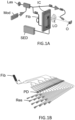
- FIGS. 3A and 3B are schematic and partial views of a heterodyne detection LIDAR imaging system of the FMCW type, suitable for determining a distance image of a scene illuminated instantaneously by a continuous and frequency modulated optical signal.
- the imaging system D here has a free space configuration ( fig.3A ) or a guided optics configuration ( fig.3B ). These are examples given for illustrative purposes, it being understood that combinations and variations of these configurations are possible.
- the imaging system D comprises a laser source SL and a shaping lens 12 for collimating the optical beam while expanding its lateral dimension.
- the optical separation device LS comprises a semi-reflecting plate or a splitter cube, here a splitter cube 31, which transmits a portion of the primary signal (laser radiation L), which becomes the object beam L o , and reflects a portion of the primary signal, which becomes the reference beam L ref .
- An optical element 21, here a transmitting diffuser is here arranged downstream of the splitter cube 31, and is adapted to make the object beam L o diverge.
- the angular aperture of the object beam L o is here such that the entire scene is uniformly illuminated by the object beam L o .
- the intensity profile of the object beam L o changes from a Gaussian profile to a flat profile.
- the same diffuser 21 here makes the object beam L o diverge.
- a lens (not shown) can be located downstream of the diffuser (or upstream thereof) so that the angular aperture has a predefined value, here a value substantially equal to the field angle of the optical imaging device lm.
- the optical recombination device SR here comprises a combiner cube 34 ensuring the transmission of the reference beam L ref and that of the reflected object beam L or in direction of the detector Det, along the same optical axis.
- the optical imaging device Im here comprises a set of lenses 41, 43 and an aperture diaphragm 42 (which defines the physical pupil) adapted to produce the image of the illuminated scene on the reception plane of the detector Det.
- the optical separation/recombination device SSR here comprises a diffuser 32 and a lens 33 located between the separator cube 31 and the combiner cube 34.
- the diffuser 32 is adapted to make the angular distribution of the intensity constant, thus obtaining a flat profile of the intensity of the reference beam L ref , and not a Gaussian profile.
- the diffuser 32 and the lens 33 shape the reference beam L ref according to a predefined angular aperture, taking into account the different optical elements present, so that the reference beam L ref effectively illuminates all the pixels of the detector Det.
- a lens 33 is not essential for this.
- the diffuser 32 and the detection plane are not conjugated, so that the image of the diffuser 32 is not formed on the detector Det.
- the optical separation/recombination device SSR is further configured to form an image, called intermediate PS, of the reference beam in a plane perpendicular to said optical axis, called intermediate image plane PI.
- the diffuser 32 is located in a plane conjugated with the intermediate image plane PI, to form the intermediate image PS (equivalent light source), which is located in the segment [MM'] (and therefore in the central zone Zc) described later.
- the imaging system D comprises a single functionalized substrate 2.
- the latter comprises a waveguide coupled to the laser source SL, which extends to a first matrix 22 of diffraction gratings (optical separation device LS).
- This matrix 22 ensures the projection of the object beam L o towards the scene.
- the waveguide propagates the reference beam L ref to a second matrix 35 of diffraction gratings (optical recombination device SR) which ensures the projection of the reference beam L ref towards the detector Det, passing through the optical imaging device lm.
- the second matrix 35 and the substrate 2 are transparent to the reflected object beam L or , such that it is transmitted and superimposed on the reference beam L ref .
- the optical separation/recombination device SSR is configured to form the intermediate image PS of the reference beam in an intermediate image plane PI perpendicular to said optical axis.
- the second array matrix 35 is located in a plane conjugate with the intermediate image plane PI, to form the intermediate image PS (equivalent light source), which is located in the segment [MM'] (and therefore in the central zone Zc).
- the array matrix 35 is located in the intermediate image plane PI and therefore itself forms the intermediate image PS (i.e. the equivalent light source of the reference beam L ref ).
- the inventors have found that the performance of the imaging system D is optimized when the presence of interference fringes produced by the coherent superposition of the reflected object beam L or with the reference beam L ref within each pixel P i is limited or even avoided. Indeed, such fringes can lead to the attenuation of the oscillations resulting from the beating of the heterodyne signal, since the pixels P i integrate all the contributions indifferently.
- the imaging system D according to the invention is configured so that the wavefronts of the two incident portions L or,i and L ref,i are similar or identical in each of the pixels P i . This makes it possible to limit the generation of interference fringes between these two incident optical beams.
- the optical separation/recombination device SSR is configured to form an image, called intermediate PS, of the reference beam L ref in a plane perpendicular to the optical axis AO, called intermediate image plane PI.
- the position of the intermediate image plane PI on the optical axis AO is included in a segment [MM'] of the optical axis corresponding to the projection on the optical axis of an intersection zone (called central zone Zc on the fig.4A to 4D , 11 And 12A-12B ) between sub-beams of the reflected object beam L or , said sub-beams being full-light field edge beams.
- Forming an image of the reference beam L ref in the intermediate image plane PI amounts to forming an equivalent light source (intermediate image PS) of the reference beam L ref .
- the equivalent light source PS is therefore located in the segment [MM'], and is advantageously contained in a central zone Zc of the rays of the reflected object beam L or of the full-light field edge.
- the equivalent light source PS has at each point an emission angle of the reference signal at least equal to the field angle of the imaging optical device Im, such that each point of the equivalent light source PS (each source point) illuminates all the pixels P i . Furthermore, the equivalent light source PS may advantageously have a lateral dimension at least equal to that of the central zone Zc of the rays of the backscattered object signal at the edge of the full-light field.
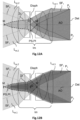
- FIGS. 4A to 4D illustrate a configuration of the imaging system D, in which an equivalent light source PS of the reference beam L ref is formed in an intermediate plane PI located at or near the aperture diaphragm Diaph.
- These figures show the reception plane of the matrix detector Det, the imaging optical device Im (lenses 41, 43 and aperture diaphragm Diaph), and the equivalent light source PS of the reference beam L ref .
- the optical separation/recombination device SSR realizes the image of the reference beam L ref in the intermediate plane PI.
- the diffuser 32 ( fig.3A ) or the network matrix 35 ( fig.3B ) is therefore located in a plane which is conjugate to the intermediate plane PI (or the array of networks 35 is itself located in the intermediate plane Pl).
- the longitudinal positioning of the equivalent light source PS along the optical axis AO and its lateral dimension can be determined by the optical properties and the dimensions of the diffuser 32 ( fig.3A ) or the network matrix 35 ( fig.3B ), and possibly by additional optical shaping elements.
- the equivalent emission angle can be determined by that of the diffuser 32 ( fig.3A ) or that of the network matrix ( fig.3B ) (and by any additional optical shaping elements).
- the wavefront of the reference beam L ref incident at each pixel P i is then made closer, or even identical, to that of the reflected object beam L or , in terms of shape and main direction. This limits the generation of interference fringes between these two optical beams, these interference fringes being likely to cause a degradation of the quality of the detected heterodyne signal.
- the pixel matrix P i of the detector Det acts as a field diaphragm.
- the field of view FOV ( Field Of View ) of the imaging optical device Im is defined as the angle in which the matrix detector Det is sensitive to the reflected object beam L or through the imaging optical device lm. It is defined here as the angle, measured at the center of the exit pupil, between two incident rays of the reflected object beam L or passing through the same central point of the exit pupil and arriving at two end pixels opposite each other with respect to the optical axis AO.
- An end pixel is a pixel P i located at the edge of the pixel matrix.
- the exit pupil is the image of the aperture diaphragm by the lenses located downstream of the latter.
- the central point is located in the plane of the aperture diaphragm.
- a central zone Zc of intersection of the edge rays of the full light field (SF1 and SF2 indicated on the fig.11 , 12A, 12B ) (unvignetted field, in English, according to the term used in the work of JE Greivenkamp titled Field Guide to Geometrical Optics, SPIE Press, Bellingham, WA (2004 )). It is defined here as the area laterally delimited by the intersection of the full-light field edge rays, i.e. the rays of the reflected object beam L or passing at the level of the outline of the aperture diaphragm Diaph and arriving at the end pixels of the pixel matrix.
- This central area Zc takes the form of two cones sharing the same base delimited by the outline of the aperture diaphragm Diaph.
- the vertices of the cones are M and M', located on the optical axis AO, respectively upstream and downstream of the aperture diaphragm Diaph. They are the longitudinal end points of the central zone Zc.
- fig.4A illustrates in detail and in part, in longitudinal section, the optical imaging device Im and the reception plane according to an alternative embodiment, in which the equivalent light source PS of the reference beam L ref is located in the central zone Zc, here upstream of the aperture diaphragm Diaph.
- the central zone Zc is illustrated more precisely in the fig.4B .
- the end pixel Px a receives here the two rays L or1 a , L or2 a of the reflected object beam L or passing through the edge of the aperture diaphragm Diaph (in the longitudinal plane), as well as the two rays L ref1 a , L ref2 a of the reference beam L ref coming from the edge of the equivalent light source PS (and of course all the rays L or which are between the rays L or1 a , L or2 a , and all the rays L ref which are between the rays L ref1 a , L ref2 a ).
- the rays L or1 a and L ref1 a both pass through the same edge of the aperture diaphragm Diaph and are therefore superimposed.
- the rays received by the second end pixel Px b we do not detail them since the situation is similar.
- the optical separation/recombination device SSR is adapted so that the equivalent light source PS has, at each of its points, a divergence cone (or equivalent emission) which covers the entire pixel matrix P i . Also, each of the pixels P i effectively receives the reference beam L ref in addition to the reflected object beam L or . The heterodyne signal is therefore formed in each pixel P i .
- the equivalent light source PS being positioned between the points M and M', and having a lateral dimension at least equal to that of the central zone Zc, the reception cone of the reference beam L ref is substantially identical to the reception cone of the reflected object beam L or , this in each pixel P i .
- fig.4B is identical to the fig.4A except that the rays of the reference beam L ref a and L ref b coming from the equivalent light source PS are not shown.
- the central zone Zc defined laterally and longitudinally by the full light field edge rays L or1 a , L or2 a and L or1 b , L or2 b (here in a longitudinal plane).
- the point M upstream of the aperture diaphragm Diaph is located on the optical axis AO and is at the intersection of the rays L or1 a and L or2 b
- the point M' downstream of the aperture diaphragm Diaph is located on the optical axis AO and is at the intersection of the rays L or2 a and L or1 b
- the largest lateral dimension of the central zone Zc is located in the plane of the aperture diaphragm Diaph.
- fig.4C is identical to the fig.4A , except that we only consider the rays received by the pixel Px a , namely the rays between the rays L or1 a and L or2 a of the reflected object beam L or , and the rays between the rays L ref1 a and L ref2 a of the reference beam L ref .
- Each point of this equivalent light source PS illuminates at least the entire reception plane, and here only the reception plane.
- the same pixel P i receives, in addition to the reflected object beam L or , the reference beam L ref coming from all the points of the equivalent light source PS.
- a principal direction is defined as being the mean direction of the angular cone of the incident beam (reference beam L ref or reflected object beam L or ) at the pixel P i considered, here at the end pixel Px a .
- an equivalent light source PS of the reference beam L ref in the central zone Zc makes it possible to reduce the angle of deviation ⁇ i at the pixel P i considered.
- This increases the dimension of the fringe gaps that can form between the reflected object beam L or and the reference beam L ref .
- the dimension of the fringe gaps is, to the first order, of the order of ⁇ /2sin ⁇ i , where ⁇ is the wavelength of the incident optical signals. Having angular cones of the optical beams (reference beam L ref and reflected object beam L or ) incident at each pixel P i that are very similar or even identical to each other also makes it possible to increase the dimension of the fringe gap.
- a propagation axis of the portion L or,i of the reflected object beam L or is collinear or substantially collinear with a propagation axis of the portion L ref,i of the reference beam L ref .
- the fringe pitch on the sensor is then ⁇ 2 sin ⁇
- the equivalent light source PS is located as close as possible to the aperture diaphragm Diaph, and that its width is at least equal and preferably substantially equal to that of the central zone Zc, therefore here to that of the orifice of the aperture diaphragm Diaph.
- the fig.4D illustrates a variation of the configuration shown in the fig.4C , in which the equivalent light source PS is located here substantially in the plane of the aperture diaphragm Diaph. It is noted that, at the pixel Px a , the end rays L or1 a and L ref1 a are coincident, as are the rays L or2 a and L ref2 a . The same is true for the rays which define the main directions of these signals. The angle of deviation ⁇ a is then substantially zero. Furthermore, since the equivalent light source PS covers substantially the entire surface of the aperture diaphragm Diaph, the angular cones of the two incident optical beams at each pixel are substantially equal.
- the wavefronts of the reflected object beam L or and the reference beam L ref are substantially identical.
- the interfringe then has a dimension that can exceed the dimensions of the pixel matrix P i , so that it can be considered that there are then no interference fringes between these optical beams likely to degrade the quality of the heterodyne signal detected by each pixel P i .
- a UT processor is connected to the detector and the laser source in order to determine the distance of the points of the scene imaged on the pixels and to construct an instantaneous distance image of the scene.
- This construction of the scene is carried out from the beat frequency F i calculated and associated with each pixel P i and from the modulation of the optical frequency of the laser radiation.
- distance image we mean here a mapping of the distance of the different points of the observed scene each corresponding to a different pixel.
- the D imaging system can thus determine an instantaneous distance image (or " global shutter " in English) where all the points of the scene are measured simultaneously with an identical start and end of measurement for all the pixels (provided that the detector Det the allows).
- the D imaging system does not require beam-steering means to scan the scene at a high frame rate.
- the measurement duration can be up to 20 ms, which relaxes the constraints on both the speed of the imager and the modulation of the optical frequency to be provided by the laser source.
- the same photon flux is obtained on the object channel on each of the pixels of the FMCW imager as on the photodetector of each pixel of the D imaging system (see figure 13 and attached passages), but with the advantage of undistorted images for moving scenes.
- the invention proposes an active distance D imaging system, with high spatial resolution (number of points in the image given by the number of pixels), robust with respect to ambient stray light, possibly of the “ global shutter ” type and capable of operating at video rate.
- the D imaging system comprises a band-pass optical filter, placed in front of the detector or in front of each pixel of the detector intended for distance detection, for example in the case of acquisition of RGB-z type images and centered on the emission wavelength of the laser in order to filter a large part of the ambient stray light.
- the equivalent light source (intermediate image) PS of the reference beam L ref is produced in the intermediate plane PI according to different variants.
- the equivalent light source PS is produced using diffraction gratings in an integrated optical circuit included in the optical recombination device generating a plurality of “source points” in the intermediate plane PI.
- the equivalent light source PS is therefore real.
- the equivalent light source PS is produced using an intermediate optical device, in free space, producing the intermediate image of the reference beam L ref .
- the equivalent light source PS is here the image of the reference beam L ref focused by a lens or an image lens group. In this embodiment, the equivalent light source PS is generally virtual.
- FIG. 5A presents an embodiment of the invention in which the optical separation device LS comprises a first integrated optical circuit OI 1 in order to reduce the vertical size of the device.
- the laser radiation L is coupled into a waveguide made with a material with a higher index than the substrate of the integrated optical circuit.
- the first integrated optical circuit OI 1 comprises a plurality of waveguides each comprising at least one diffraction grating, called an object grating, separating the two reference/object paths.
- the object gratings are adapted so as to extract vertically (or more generally, extracting out of the plane of the circuit OI1) a part of the light from the waveguide, forming the object beam L o , the other part continuing its propagation in at least one waveguide and forming the reference beam L ref .
- the use of a plurality of diffraction gratings makes it possible to improve the uniformity or to adjust the wavefront of the object beam L o , while respecting a phase condition between the different gratings in order to be able to form a coherent superposition of the reference beam L ref and the reflected object beam L or on the detector Det.
- the first integrated optical circuit OI 1 comprises a single diffraction grating on a single waveguide.
- the optical projection device Proj can be adapted to project light onto the scene to be illuminated, the image of which will then be formed on the detector, for example a rectangular scene.
- the optical projection device Proj illuminates the scene according to a cone of angular aperture substantially equal to the field angle of the optical imaging device Im (which is determined by its focal length and the size of the imager).
- the optical imaging device Im which is determined by its focal length and the size of the imager.
- the optical projection device Proj is preferably adapted to illuminate the scene uniformly, to subsequently ensure uniform illumination and a signal-to-noise ratio on the detector, in particular in the case where the scene is Lambertian.
- substantially uniform it is meant here that the standard deviation of the light intensity on the scene is for example less than 25% of the average of the light intensity.
- the optical projection device Proj comprises a conventional two-stage optical device formed of a first collimation lens LP 1 , and a second lens LP 2 which makes the image of the first lens on the scene (for example, the first lens is approximately at the object focus of the second lens LP 2 to avoid the image of the source on the scene which is almost at infinity).
- the laser source SL is at the object focus of the collimation lens LP 1 .
- the lens assembly LP 1 , LP 2 is folded to reduce the vertical size of the optical projection device Proj and therefore comprises two mirrors Mi 1 , and Mi 2 arranged at 45°.
- the imaging system D further comprises a shaping optical device DOE ( Diffractive Optical Element ) comprising periodic patterns, the period of which is of the order of the wavelength of the laser radiation.
- the optical device DOE is arranged after the projection optical device Proj in order to improve the uniformity of the illumination of the scene.
- the optical device DOE can be omitted and the beam shaping can be performed by the projection optical device Proj.
- the projection optical device Proj and the shaping optical device DOE can be used alone or in combination in all embodiments of the invention.
- FIG. 5B represents a schematic view of an optical recombination device SR according to an embodiment of the invention.
- the optical recombination device SR comprises an integrated optical circuit OI 2 , called the second integrated optical circuit, in order to reduce the vertical size of the optical device SR.
- the reference beam L ref is coupled into the second integrated optical circuit OI 2 by means of an optical element FO (not shown).
- the second integrated optical circuit OI 2 comprises at least one waveguide and at least one diffraction grating called the reference grating RR for extracting the light in the direction of the detector Det through at least part of the optical imaging device lm.
- the reference grating RR makes it possible to generate the equivalent of a source point constituting the intermediate image PS on the reference path, near the aperture diaphragm of the optical imaging device lm.
- the second integrated optical circuit OI 2 is arranged in said intermediate image plane PI so that the reference network RR forms the intermediate image PS.
- the RR reference grating here is a High Contrast Grating (HCG) type grating, which allows light to be decoupled preferentially on one side of the waveguide (on the Figure 5B , to the imaging optical device Im).
- HCG High Contrast Grating
- the lateral dimensions of the reference grating RR are reduced (about a few wavelengths of the laser radiation L) to allow an appropriate divergence of the reference beam L ref from the reference grating RR and a wide illumination of the pupil to illuminate the entire detector Det.
- the reflected object beam L or is only slightly affected by the insertion of a waveguide and the grating RR in the light path.
- the refractive index contrast of the gratings and the waveguides remains low, and the diffraction gratings are not imaged on the detector Det.
- the waveguide is not located in a conjugate plane of the detector Det, and therefore does not impact the formation of the image on the detector Det.
- the substrate on which the waveguide is produced can be inserted between two lenses of the optical imaging device Im, when the latter comprises at least two lenses.
- the waveguide and the RR network of the second integrated optical circuit OI 2 are produced on a surface of the or one of the lenses of the optical imaging device lm.
- the losses by diffraction of the flow are then low since the waveguide is of small lateral dimension and is not imaged on the detector Det, and the surface of the RR network is small compared to the surface of the pupil.
- the reference beam L ref is recombined with the reflected object beam L or by a plurality of reference diffraction gratings. There is then a phase relationship between the reference gratings so that they are adapted to create a wavefront on the pixels of the Det detector whose tangent at each point does not make an angle greater than ⁇ 2 has pix relative to the tangent of the wavefront of the reflected object beam L or .
- the guides of the circuit OI 2 are advantageously single-mode.
- the circuit OI 2 comprises active or inactive phase shifters in the waveguides or at the output of the reference grating. Each diffraction grating behaves like a secondary source.
- the gratings are arranged regularly to form a matrix of lines and columns, preferably of the same period.
- the light diffracted by all of the gratings forms regularly spaced light patterns in the plane of the detector Det, with one pattern per pixel.
- the advantage of having a plurality of reference gratings is to be able to better distribute the light patterns, better control the uniformity of the illumination of the detector by the secondary source points and better adjust the wavefront of the reference beam L ref relative to the wavefront of the reflected object beam L or on the detector Det.
- the guided reference beam L ref is decoupled in the direction of free space towards the optical imaging device Im using a semi-reflecting plate included in the waveguide and oriented here at 45° to the propagation axis in the waveguide.
- the advantage of the embodiment with a grating is to reduce the flux losses on the reference path compared to the embodiment with a semi-reflecting plate.
- the SR recombination optical device makes it possible to reduce the total thickness of the imaging system D since a bulky micro-optical component (for example a semi-reflecting plate whose vertical size is approximately equal to the diameter of the entrance pupil of the imaging optical device lm) is replaced by a simple substrate with a thickness close to or less than a millimeter.
- a bulky micro-optical component for example a semi-reflecting plate whose vertical size is approximately equal to the diameter of the entrance pupil of the imaging optical device lm
- FIG. 6 illustrates a schematic view of an imaging system D according to a first embodiment of the invention.
- This embodiment combines the optical separation device LS of the Figure 5A and the SR optical recombination device of the Figure 5B .
- An optical fiber FO is adapted to guide the reference beam L ref from the first integrated optical circuit OI 1 to the second integrated optical circuit OI 2 .
- the use of the two integrated optical circuits OI 1 , OI 2 makes it possible to reduce the vertical size of the imaging system D.
- the imaging system D here comprises the optical projection device Proj and the optical shaping device DOE in order to obtain uniform illumination on the scene.
- the second integrated optical circuit OI 2 comprises a plurality of reference gratings.
- the optical separation/recombination device therefore comprises the integrated optical circuit OI 3 into which the laser radiation L is coupled.
- At least one waveguide of the integrated circuit called the reference waveguide GR guides the reference beam L ref towards the optical recombination device SR comprising at least one reference grating RR, located on the reference waveguide.
- the integrated optical circuit OI 3 is arranged in said intermediate image plane such that the reference grating forms the intermediate image PS.
- the optical recombination device SR here comprises a plurality of reference gratings.
- the optical recombination device SR comprises a single reference grating.
- This embodiment has the advantage of avoiding flux losses caused by the coupling/decoupling of the reference beam L ref in the optical fiber FO of the imaging system D of the figure 6 .
- this arrangement helps to reduce the complexity of the system and its size.
- the reference network(s) RR are configured so that the divergence of the source points is equal or approximately equal to the angle between the sub-beams SF1, SF2 (cf. fig.11 ) of the reflected object beam L or the edge of the full light field of the imaging optical device Im, in the space where the plane of the source points is located, i.e. in the intermediate plane PI. This condition makes it possible to optimize the photometry of the system.
- the optical separation/recombination device SSR further comprises an intermediate optical device SI, arranged after the optical separation device LS, and before the optical recombination device SR.
- This intermediate optical device Si is adapted to focus the reference beam L ref and to form the intermediate image PS (equivalent light source) in the intermediate plane PI.
- this intermediate optical device Si is a lens or a set of lenses.
- the intermediate optical device Si makes it possible to shape the reference beam L ref by making it converge towards the optical imaging device Im, so that the reference beam L ref illuminates the entire detector Det, and so that the wavefronts of the reflected object beams L or and reference beams L ref at each pixel are similar or even identical.
- the optical separation device LS and the optical recombination device SR may be a splitter cube or a splitter blade.
- an assembly similar to that of the embodiment of the Figure 5A formed by an optical projection device Proj and an optical shaping element DOE, allows the scene to be illuminated in a substantially uniform manner.
- the assembly formed by the optical projection device Proj and the optical shaping element DOE is placed downstream of the optical separation device LS, on the path of the object beam L o .
- FIG 9 illustrates a schematic view of an imaging system D according to another embodiment of this second variant of the invention.
- This embodiment is identical to that of the figure 8 except that here the imaging optical device Im is vertical and the detector Det is horizontal, in order to save horizontal space at the level of the complete imaging system D.
- the separation optical device LS can here be a splitter plate replacing the second mirror Mi 2 oriented here at 45°, which avoids having to position it above the projection optical device Proj.
- the laser source SL is configured to emit vertically, to further save horizontal space.
- the first mirror Mi 1 of the folded projection optical device Proj is then removed and the laser source SL emits the laser radiation vertically towards the separation optical device LS through the collimation lens LP 1 .
- This embodiment is compatible with a longer focal length since the thickness of the imaging optical device Im is not limited by the width of the imaging system D. Thus, the angular resolution is greater, giving access to more details in the image (but with a more limited field of view).
- the imaging system D uses the FMCW technique, and the laser source therefore operates in continuous wave emission.
- the laser source SL can here be configured so that the optical frequency is modulated by a periodic linear ramp of excursion B and duration T.
- the detector is a matrix of pixels specialized for FMCW heterodyne detection with photodetection and signal processing integrated in each pixel, which provides the beat frequency at the end of the frame time (20 ms for the frame time of the video rate).
- each pixel advantageously comprises, below a photodetector layer CP comprising the photodetector Ph, a so-called interconnection layer BE in a dielectric material transparent to the recombined beam.
- the interconnection layer BE comprises metal interconnections Met connected to the electronic circuit CE and to the processor UT.
- Different peak detection techniques can be implemented, such as, for example, a comparison with respect to a predetermined level, or a comparison of a sample with its two nearest neighbors, this method being more robust with respect to low frequency noise.
- the metal interconnections transmit to the processor a signal representative of the count of the number of detected periods.
- the distance resolution is ⁇ z ⁇ c 2 B .
- the sampling frequency of pixel P i is greater than twice, preferably three times the frequency F R,max .
- the optical coupling in the photodetector present in each pixel P i is essentially vertical, i.e. the light from the reference and object channels propagates in the thickness of the photodetector layer CP.
- the output data stream of the Det detector can be similar to that of a standard image sensor operating at video frame rate, with the illumination information replaced by frequency information.
- the light incident on the pixel P i is focused on the photodetector by a microlens ML if the fill factor of the pixel P i is less than 1.
- a factor may be desirable in order to avoid crosstalk (spreading of light) between adjacent pixels of the detector Det.
- elements are arranged in the photodetector layer CP, between each pixel P i , in order to individualize areas of the photodetector layer.
- the microlenses may be contiguous, attached to a surface of the pixel matrix and adapted to optimize a collection of the reflected object beam L or and the reference beam L ref on the pixels.
- the laser source SL is an edge emitting laser (EEL) or a vertical-cavity surface- emitting laser (VCSEL) and the photodetector is a photodiode or an avalanche photodiode.
- the laser source is a quantum cascade laser (QCL) and the photodetector is a bolometer array or a mercury-cadmium telluride (MCT) infrared photodetector.
- QCL quantum cascade laser
- MCT mercury-cadmium telluride
- Free space optics means the propagation of an optical beam through lenses, beam splitters, and cubes.
- Integrated optics means the propagation of an optical beam through waveguides, and diffraction gratings of integrated optics circuits.
- FIG 11 shows an illustration of the overlap of the reflected object beam L or by the reference beam L ref on the detector Det, in one embodiment of the imaging system D.
- the imaging optical device Im is a thin lens, with an aperture diaphragm Diaph located on this lens. This figure is similar to the fig.4B .
- the optical separation/recombination device SSR is configured so that the longitudinal positions (i.e. that of the intermediate image plane PI) and lateral positions of the intermediate image PS relative to the optical axis lead to the direction of the rays of the reference beam L ref tending as closely as possible to that of the rays of the reflected object beam L or .
- the sub-beam SF 1 (also called L or,1 ) is the portion of the reflected object beam L or that illuminates the pixel P1. It is a sub-beam parallel and inclined with respect to the optical axis, coming from a source point of the scene considered located for example at infinity from the point of view of the optical imaging device !m.
- the subbeam L ref,1 is the portion of the reference beam L ref that reaches the considered pixel P 1 .
- Each ray of this subbeam comes from a different source point. In the object space of the optical imaging device Im, these rays are parallel to the inclined subbeam of the reflected object beam L or since they pass through the same optical imaging device lm.
- the longitudinal position of the intermediate image PS on the optical axis AO is therefore included in the segment [MM'].
- the segment [MM'] was defined above in connection with the fig.4A to 4D .
- the reference beam L ref from the optical separation/recombination device SSR has at least one lens of the imaging optical device Im in common with the reflected object beam L or so that these two beams can be superimposed on the detector Det.
- the segment [MM'] corresponds to the projection on the optical axis of the central zone Zc of the two sub-beams SF 1 , SF 2 of the reflected object beam at the edge of the full light field.
- the intermediate image plane PI is located upstream of the aperture diaphragm Diaph of the imaging optical device !m.
- Source points of the intermediate image PS which would be placed in the intermediate plane PI but beyond, on either side of the segment [S1S2] would only partially illuminate the detector Det.
- the source points of an intermediate image which would be located too far upstream of the point M on the optical axis AO would only partially illuminate the detector Det.
- the lateral dimension of the intermediate image PS from the photometric point of view is advantageously less than or equal to the lateral dimension of the intersection of the sub-beams SF 1 , SF 2 , at the intermediate image plane PI.
- An advantageous dimension is represented by the segment [S1S2].
- the overlap of the angular spectra of the reflected object beam L or and the reference beam L ref on a given pixel is greater if the aperture AP of the imaging optical device Im is small compared to its field angle of the reflected object path FOV, this field angle being equal to the divergence of the reflected object beam L or .
- These two angular spectra are centered for the pixel of the detector Det located on the optical axis AO.
- the intermediate image plane PI is located in the plane of the thin lens with a diameter equal to the pupil, the wavefronts of the reflected object beams L or and reference beams L ref are merged. As indicated above, the quality of the detected heterodyne signal is then greatly improved.
- the optical separation/recombination device SSR is configured such that a divergence of the reference beam L ref from the optical separation/recombination device SSR is equal to the angle formed by said sub-beams SF 1 , SF 2 at the intermediate image plane PI.
- the reference beam L ref from the optical separation/recombination device SSR illuminates all of the pixels of the detector Det.
- the optical recombination device SR is configured such that the reference grating(s) form source points with a divergence equal to the field angle of the reflected object beam L or at the intermediate image plane PI.
- the optical separation/recombination device SSR is configured so that the intermediate image plane PI is located close to or coincides with a plane comprising a pupil or an aperture diaphragm Diaph of the optical imaging device Im, to improve the uniformity of the illumination on the detector but also to improve the quality of the detected heterodyne signal.
- the intermediate plane PI is merged with a plane comprising a pupil or an aperture diaphragm Diaph of the optical imaging device lm.
- This embodiment makes it possible to minimize the average angle of the wavefront of the object beam. reflected L or and that of the wavefront of the reference beam L ref on each pixel.
- the angular difference between the reflected object beam L or and the reference beam L ref on each pixel is small enough to generate flat-tone fringes.
- flat-tone here we mean that there is no visible fringe on the pixels.
- the interfringe is large compared to the size of the pixels (here to the size of the microlenses).
- the intermediate image plane PI can however be located upstream of the optical imaging device Im and its pupil. This position allows greater accessibility of the intermediate image PI, which can be advantageous in the case of a guided optics configuration of the imaging system D (cf. fig. 5B , 6 And 7 ).
- the intermediate image plane PI can also be located downstream of the pupil of the optical imaging device Im, while keeping at least one lens of the optical imaging device Im in common between the reflected object beam L or and the reference beam L ref , in order to generate an equivalent light source PI (here virtual).
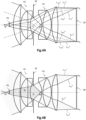
- FIGS. 12A and 12B illustrate an example of overlap of the reflected object beam L or and the reference beam L ref on the detector Det, for an optical imaging device Im of the triple Gauss type.
- the intermediate image plane PI is located respectively on the plane of the aperture diaphragm Diaph and in front of the first group of lenses of the optical imaging device lm. It is understood that the optical imaging device Im is not limited to a triple Gauss but can be any other objective known to those skilled in the art.
- the two sub-beams SF 1 and SF 2 are here the beams at the edge of the full light field of the reflected object beam L or , illuminating respectively the pixels P 1 and P 2 of the detector Det.
- the lateral dimension of the intermediate image PI is given by the segment [S1S2], that is to say the lateral dimension of the intersection of the sub-beams SF 1 , SF 2 , at the intermediate image plane PI. Emission cones of similar divergence of 3 source points are illustrated as an example.
- the sub-beam L ref,1 which is the portion of the reference beam L ref which reaches the considered pixel P 1 .
- the configuration of the Figure 12B is advantageous from the point of view of the structural accessibility of the intermediate image plane PI (in particular in the guided optics configuration), whereas the configuration of the Figure 12A is more optimal to ensure obtaining flat-tone interference on the pixel matrix.
- the angular deviation between the reference beam L ref,1 and the sub-beam SF 1 of the reflected object beam L or,1 is smaller in configuration 12A than in configuration 12B.
- FIG 13 represents different elements of the imaging system D according to one embodiment, and highlights the effect of the speckle grains on the detection of the heterodyne signal.
- the observed scene Obj always has a certain degree of roughness in practice. Since the imaging system D is based on coherent imaging, a speckle figure (laser granulation) is therefore formed in the image focal plane of the detector Det. The characteristic size of the speckle grains can then impact the quality of the measurement of the detected heterodyne signal.
- the phase of the reflected object beam is substantially constant within a speckle grain, but is random between the different speckle grains.
- the oscillations of the heterodyne signal generated by interference between the reflected object beam and the reference beam are at the same frequency for neighboring speckle grains, but are randomly phase-shifted between the speckle grains.
- the photodiode which indifferently integrates all the contributions will provide an averaged signal with a weakened AC component, or even eliminated (for example in the case of two speckle grains in phase opposition: cf. fig. 11 : case ⁇ g ⁇ a pix ).
- ⁇ g is the average size of a speckle grain in the plane of the detector Det
- a pix is the lateral size of a pixel (e.g. here of a microlens located above a photodiode).
- the diameter ⁇ g of the speckle grains is greater than the size a pix of the photodetector (cf. fig. 11 : case ⁇ g > a pix )
- the contrast of the oscillations is greater, and therefore more favorable to good detection of the heterodyne signal.
- the surface (or size) of the photodetector is smaller than the surface (or average size) of the speckle grains.
- the average speckle grain size ⁇ g in the image of a scattering object has a statistical average of 2 ⁇ f # , where ⁇ is the wavelength of the laser source, and f # is the aperture number of the imaging optical device lm.
- the numerical aperture of the imaging optical device Im is adapted so that the average size ⁇ g of the speckle grains on the detector Det is greater than a characteristic dimension a pix of the photodetector of each pixel of the detector.
- characteristic dimension is meant for example the side of a square photodetector (here the side of the associated microlens).
- the following passage describes typical parameters and performances of the D imaging system according to one embodiment of the invention.
- the value of the parameters used is not limiting and is given as an example.
- the desired distance resolution is assumed to be 5cm, which sets the laser optical frequency excursion to B ⁇ c 2 ⁇ ⁇ 3 GHz .
- the duration T of the optical frequency ramp of the source is therefore 20ms.
- the duration T of the ramp can be a sub-multiple of 20ms, to be able to make several ramps in this duration T, establish a measurement statistic and thus improve the precision of the measurements.
- this is only possible if the signal and the signal-to-noise ratio are sufficient.
- the slope of the ramp is 0.15MHz/ ⁇ s, which is a value easily accessible by modulating the injection current of a semiconductor laser.
- the pixel size is then 5 ⁇ 5 ⁇ m.
- the aperture number f # of the imaging optical device Im is preferably greater than 1.9, thus having a characteristic speckle grain size ⁇ g in the image plane greater than the pixel size a pix of the detector Det.
- f # 2 is chosen with a pupil Diaph of the imaging optical device Im of 3.5mm.
- the laser power of the object beam L o is equal to, for example, 10 mW, a value that complies with the ocular safety standard at 1300 nm.
- a ratio of Ts equal to 95%/5% between the emitted powers of the object/reference channels, which gives a power of 0.5 mW on the reference beam L ref .
- the fraction of power of the portion L or,i of the reflected object beam incident on each pixel P i with respect to the emitted object power is 10 -15 .
- This ratio is very low despite the relatively large aperture of the imaging optical device Im, since a large part of the light of the object path is scattered outside the pupil of this optic, the portion passing through the pupil being then shared between all the pixels P i of the detector Det.
- the fraction of the power of the reference path incident in each pixel is clearly higher, of the order here of 10 -6 .
- the photodetector Ph is an InGaAs photodiode with a quantum efficiency QE of 70% at 1300nm. Furthermore, in order to respect Shannon's theorem, the integration time (inverse of the sampling frequency) is equal to one third of a period 1/f R .
- the continuous component DC of the detected signal i.e. the electronic signal of the average incident flux of the object channel and the reference channel on the pixel
- F DC 13000 electrons.
- the alternating component AC i.e. the useful signal F AC , (the electronic signal representing the beat) modulated at the frequency f Rmax , carrying the distance information, varies between 15 and 140 electrons depending on the (unpredictable) positioning of the integration times in the sinusoidal signal.
- the dominant noise is the photon noise of the reference channel at each pixel, corresponding to approximately 100 electrons (equal to F DC ) in the integration time.
- the photon noise of the ambient stray light F amb is lower (20 electrons of noise with sunlight filtered through a 50nm bandpass filter centered on the laser wavelength).
- the dark current noise about 10 electrons with a dark current of 1pA
- the readout noise a few electrons
- the signal-to-noise ratio of the order of 1 or even lower, is compatible with the detection and counting of peaks in the useful signal F AC .
- the signal-to-noise ratio is similar.
- the detector should have a bandwidth of at least 10GHz, which is possible but restrictive, and the laser source should be able to be wavelength modulated at a frequency of several tens of MHz with a modulation amplitude of several GHz. as explained above.
- the illumination device must scan the scene at a rate of several MHz.
Landscapes
- Engineering & Computer Science (AREA)
- Physics & Mathematics (AREA)
- Computer Networks & Wireless Communication (AREA)
- General Physics & Mathematics (AREA)
- Radar, Positioning & Navigation (AREA)
- Remote Sensing (AREA)
- Electromagnetism (AREA)
- Optical Radar Systems And Details Thereof (AREA)
Claims (17)
- Kohärentes LIDAR-Abbildungssystem (D), umfassend:- eine Laserquelle (SL), die so konfiguriert ist, dass sie Laserstrahlung (L) mit einer zeitlich modulierten optischen Frequenz (FL) aussendet;- ein optisches Gerät zur Trennung/Rekombination (SSR), das mindestens Folgendes umfasst:-- ein optisches Gerät zur Trennung (LS), das die Laserstrahlung (L) räumlich in einen sogenannten Referenzstrahl (Lref), der auf ein optisches Abbildungsgerät (Im) gerichtet ist, und in einen sogenannten Objektstrahl (Lo), der auf eine zu beleuchtende Szene (Obj) gerichtet ist, aufteilen kann;-- ein optisches Gerät zur Rekombination (SR), das den Referenzstrahl (Lref) räumlich mit einem Teil des von der Szene reflektierten Objektstrahls, dem reflektierten Objektstrahl (Lor), überlagern kann;- das optische Abbildungsgerät (Im) eine optische Achse (AO) aufweist und ein Bild der beleuchteten Szene auf einem Detektor (Det) durch Fokussieren des reflektierten Objektstrahls (Lor) erzeugt,- der Detektor (Det) eine Matrix von Pixeln Pi, i ∈ [1,n] umfasst, wobei jedes der Pixel Pi einen Fotodetektor (Ph) umfasst, der einen Abschnitt (Lor,i) des reflektierten Objektstrahls (Lor) und einen Abschnitt (Lref,i) des Referenzstrahls (Lref) erfassen kann, die zusammen einen Abschnitt eines rekombinierten Strahls (Lrec) bilden, der eine Überlagerungsfrequenz aufweist, die für einen Abstand von der beleuchteten Szene repräsentativ ist;- einen Prozessor (UT), der mit dem Detektor (Det) und der Laserquelle (SL) verbunden ist und konfiguriert ist, um eine Entfernung von Punkten der Szene, die auf den Pixeln abgebildet sind, zu bestimmen und ein Entfernungsbild der Szene aus der Überlagerungsfrequenz (Fi), die mit jedem Pixel Pi verbunden ist, und aus der modulierten optischen Frequenz der Laserstrahlung zu konstruieren;- dadurch gekennzeichnet, dass-- das optische Gerät zur Trennung/Rekombination (SSR) ferner so konfiguriert ist, dass es ein sogenanntes Zwischenbild (PS) des Referenzstrahls (Lref) in einer Ebene senkrecht zur optischen Achse, der sogenannten Zwischenbildebene (PI), bildet,--- die Position der Zwischenbildebene (PI) auf der optischen Achse (AO) innerhalb eines Segments (MM') entlang der optischen Achse liegt, das der Projektion einer Kreuzungszone (Zc) zwischen Teilstrahlen des reflektierten Objektstrahls (Lor) auf die optische Achse entspricht, wobei die Teilstrahlen Volllichtfeldrandstrahlen sind.
- Abbildungssystem (D) nach Anspruch 1, wobei das optische Gerät zur Trennung/Rekombination (SSR) so konfiguriert ist, dass die Zwischenbildebene (PI) mit einer Ebene zusammenfällt, die eine Pupille oder eine Aperturblende des optischen Abbildungsgeräts (Im) enthält.
- Abbildungssystem (D) nach einem der Ansprüche 1 bis 2, wobei das optische Gerät zur Trennung/Rekombination (SSR) so konfiguriert ist, dass eine seitliche Abmessung des Zwischenbildes (PS) kleiner oder gleich einer seitlichen Abmessung des Schnittpunktes der Teilstrahlen in der Zwischenbildebene (PI) ist.
- Abbildungssystem (D) nach einem der Ansprüche 1 bis 3, wobei das optische Gerät zur Trennung/Rekombination (SSR) so konfiguriert ist, dass eine Divergenz des Referenzstrahls (Lref) aus dem optischen Gerät zur Trennung/Rekombination gleich einem Winkel ist, der von den Teilstrahlen in der Zwischenbildebene (PI) gebildet wird.
- Abbildungssystem (D) nach einem der Ansprüche 1 bis 4, wobei das optische Gerät zur Trennung/Rekombination (SSR) so konfiguriert ist, dass für jedes Pixel Pi eine Ausbreitungsachse des Abschnitts (Lor,i) des reflektierten Objektstrahls (Lor), mit einer Ausbreitungsachse des Abschnitts (Lref,i) des Referenzstrahls einen Winkel θ bildet, sodass θ < λ/(2×apix), wobei apix eine charakteristische Dimension des Photodetektors jedes Pixels des Detektors ist, und λ die Wellenlänge der Laserstrahlung (L) ist.
- Abbildungssystem (D) nach einem der Ansprüche 1 bis 5, umfassend ein optisches Gerät zur Formgebung (DOE), das im Weg der Laserstrahlung oder des Objektstrahls (Lo) angeordnet ist und so konfiguriert ist, dass ein Strahl aus dem optischen Gerät zur Formgebung (DOE) eine gleichmäßige Beleuchtung der zu beobachtenden Szene aufweist.
- Abbildungssystem (D) nach einem der Ansprüche 1 bis 6, wobei das optische Abbildungsgerät (Im) eine solche numerische Apertur aufweist, dass ein Durchmesser ϕg von Streukörnern auf dem Detektor (Det) größer ist als eine charakteristische Abmessung apix des Photodetektors jedes Pixels Pi des Detektors (Det).
- Abbildungssystem (D) nach einem der Ansprüche 1 bis 7, wobei die Laserquelle (SL) so konfiguriert ist, dass die optische Frequenz durch eine periodische lineare Rampe mit der Auslenkung B und der Dauer T moduliert wird, und dass eine Kohärenzlänge der Laserstrahlung doppelt so groß ist wie ein maximaler vorbestimmter Abstand zmax zwischen der zu beleuchtenden Szene (Obj) und dem Abbildungssystem (D).
- Abbildungssystem (D) nach einem der Ansprüche 1 bis 8, wobei jedes Pixel Pi eine elektronische Verarbeitungsschaltung (CE) umfasst, die geeignet ist, die Überlagerungsfrequenz Fi des Abschnitts des rekombinierten Strahls (Lrec) zu berechnen.
- Abbildungssystem (D) nach Anspruch 9, wobei die Berechnung der Überlagerungsfrequenz Fi für alle Pixel Pi des Detektors (Det) gleichzeitig erfolgt, wobei jedes Pixel Pi eine sogenannte Zwischenverbindungsschicht aus einem dielektrischen Material umfasst, das für den rekombinierten Strahl (Lrec) transparent ist, wobei die Zwischenverbindungsschicht metallische Zwischenverbindungen (Met) umfasst, die mit der elektronischen Schaltung (CE) verbunden sind, wobei die Verbindungsschicht auf einer Seite des Fotodetektors angeordnet ist, die einer Seite gegenüberliegt, die den Abschnitt (Lor,i) des rekombinierten Strahls (Lrec) darstellt, wobei die dem Pixel Pi zugeordnete elektronische Schaltung so konfiguriert ist, dass sie einen im Fotodetektor (Ph) erzeugten Fotostrom, der die Überlagerungsfrequenz Fi darstellt, sammelt, um ihn in eine Spannung umzuwandeln und dann:- Ersetzen einer DC-Komponente des die Überlagerungsfrequenz darstellenden Signals durch einen vorbestimmten festen Spannungswert, wodurch ein elektrisches Signal, das substituierte Signal, erzeugt wird; und dann- Verstärken des substituierten Signals, wodurch ein verstärktes Signal erzeugt wird;- Erkennen von Spitzen, steigenden oder fallenden Flanken des verstärkten Signals mit Hilfe eines Komparators,- Durchführen einer Zählung (Sig) der Anzahl der erkannten Perioden, Übertragen eines Signals, das für die Zählung der Anzahl der erkannten Perioden repräsentativ ist, an den Prozessor,- wobei der Prozessor die Entfernung eines Punktes der Szene bestimmt, indem er die Anzahl N von Perioden, die während der Dauer T der Modulation der optischen Frequenz erfasst werden, aus dem repräsentativen Zählsignal berechnet.
- Abbildungssystem (D) nach Anspruch 9 oder 10, wobei eine Pixelabtastfrequenz größer als das Zweifache, vorzugsweise das Dreifache, einer Frequenz FR,max ist, die der Überlagerungsfrequenz entspricht, die mit einem Szenenobjekt verbunden ist, das sich in einem maximalen vorbestimmten Abstand zmax befindet, und derart, dass FR,max = 2Bzmax /cT, mit c die Lichtgeschwindigkeit, und wobei die Laserquelle (SL) so konfiguriert ist, dass die optische Frequenz durch eine periodische lineare Rampe mit der Auslenkung B und der Dauer T moduliert wird.
- Abbildungssystem (D) nach einem der Ansprüche 1 bis 11, wobei das optische Abbildungsgerät (LS) eine integrierte optische Schaltung, die erste integrierte optische Schaltung genannt wird, umfasst, in die die Laserstrahlung eingekoppelt wird, wobei mindestens ein Wellenleiter der ersten integrierten Schaltung den Referenzstrahl (Lref) führt, wobei die erste integrierte optische Schaltung ferner eine Vielzahl von Wellenleitern umfasst, von denen jeder mindestens ein Beugungsgitter, das Objektgitter genannt wird, umfasst, um den Objektstrahl (Lo) zu formen.
- Abbildungssystem (D) nach einem der Ansprüche 1 bis 12, wobei das optische Gerät zur Rekombination (SR) eine integrierte optische Schaltung umfasst, die zweite integrierte optische Schaltung (OI2) genannt wird, in die der Referenzstrahl (Lref) mit Hilfe eines optischen Elements (FO) eingekoppelt wird, die zweite integrierte optische Schaltung mindestens einen Wellenleiter mit mindestens einem Beugungsgitter umfasst, das als Referenzgitter (RR) bezeichnet wird, wobei das Referenzgitter den Referenzstrahl in den freien Raum und in das optische Gerät zur Formgebung (Im) koppelt, wobei die zweite integrierte optische Schaltung (OI2) in der Zwischenbildebene so angeordnet ist, dass das Referenzgitter das Zwischenbild (PS) formt.
- Abbildungssystem (D) nach Anspruch 12 und 13, wobei das optische Element eine optische Faser (FO) ist, die den Referenzstrahl von der ersten integrierten optischen Schaltung zu der zweiten integrierten optischen Schaltung führt.
- Abbildungssystem (D) nach einem der Ansprüche 1 bis 11, wobei das optische Gerät zur Trennung/Rekombination eine integrierte optische Schaltung umfasst, in welche die Laserstrahlung eingekoppelt wird, wobei die integrierte optische Schaltung das optische Gerät zur Trennung (LS) und das optische Gerät zur Rekombination (SR) umfasst,- das optische Gerät zur Trennung (LS) eine Vielzahl von Wellenleitern der integrierten optischen Schaltung umfasst und jeder mindestens ein Beugungsgitter, das so genannte Objektgitter, umfasst, wobei die Objektgitter den Objektstrahl in den freien Raum und das zu beobachtende Szenenobjekt koppeln,- mindestens ein Wellenleiter der integrierten Schaltung, der als Referenzwellenleiter (GR) bezeichnet wird, den Referenzstrahl (Lref) zu dem optischen Gerät zur Rekombination (SR) führt, das mindestens ein Beugungsgitter, das als Referenzgitter (RR) bezeichnet wird, enthält, das sich auf dem Referenzwellenleiter befindet, wobei die integrierte optische Schaltung in der Zwischenbildebene so angeordnet ist, dass das Referenzgitter das Zwischenbild (PS) bildet.
- Abbildungssystem (D) nach einem der Ansprüche 1 bis 11, wobei das optische Gerät zur Trennung/Rekombination ferner ein optisches Zwischengerät (SI) umfasst, das nach dem optischen Gerät zur Trennung (LS) und vor dem optischen Gerät zur Rekombination (SR) angeordnet ist, wobei das optische Zwischengerät (SI) so beschaffen ist, dass es den Referenzstrahl fokussiert und das Zwischenbild bildet.
- Verfahren zum Abbilden durch ein kohärentes Abbildungssystem (D) LIDAR, umfassend die folgenden Schritte:- Emittieren von Laserstrahlung (L) von einer Laserquelle (SL) mit einer zeitlich modulierten optischen Frequenz (FL);- Trennen der Laserstrahlung (L) durch ein optisches Gerät zurTrennung (LS) eines optischen Geräts zur Trennung/Rekombination (SSR) räumlich in einen als Referenzstrahl (Lref) bezeichneten Strahl und in einen als Objektstrahl (Lo) bezeichneten Strahl, der auf ein zu beleuchtendes Szenenobjekt (Obj) gerichtet ist;- Überlagern eines von der Szene reflektierten Objektstrahls, des so genannten reflektierten Objektstrahls (Lor), und des Referenzstrahls (Lref) durch ein optisches Gerät zur Trennung/Rekombination (SR) des optischen Geräts zur Rekombination (SSR) in räumlicher Hinsicht;- Erstellen, durch ein optisches Abbildungsgerät (Im), eines Bildes des Szenenobjekts auf einem Detektor (Det) durch Fokussieren des reflektierten Objektstrahls, wobei der Detektor (Det) eine Matrix aus einer Vielzahl von Pixeln Pi, i ∈ [1,n] umfasst;- Erkennen, auf jedem der Pixel Pi, eines Abschnitts (Lor,i) des reflektierten Objektstrahls (Lor) und eines Abschnitts (Lref) des Referenzstrahls (Lref), die zusammen einen Abschnitt eines rekombinierten Strahls (Lrec) bilden, der eine Überlagerungsfrequenz aufweist, die für eine Entfernung des beleuchteten Szenenobjekts repräsentativ ist;- Bestimmen, durch einen Prozessor (UT), der mit dem Detektor (Det) und der Laserquelle (SL) verbunden ist, einer Entfernung von Punkten der Szene, die auf den Pixeln abgebildet sind, und Konstruieren eines Entfernungsbildes der Szene, ausgehend von der Überlagerungsfrequenz (Fi), die jedem Pixel (Pi) zugeordnet ist, und ausgehend von der modulierten optischen Frequenz der Laserstrahlung,dadurch gekennzeichnet, dass:
das optische Gerät zur Trennung/Rekombination (SSR) so konfiguriert ist, dass es ein Bild, das so genannte Zwischenbild (PS), des Referenzstrahls (Lref) in einer Ebene senkrecht zur optischen Achse, der so genannten Zwischenbildebene (PI), bildet, wobei die Position der Zwischenbildebene (PI) auf der optischen Achse (AO) in einem Segment (MM') entlang der optischen Achse enthalten ist, das der Projektion einer Schnittpunktzone zwischen Volllichtfeldrandstrahlen des reflektierten Objektstrahls (Lor) auf die optische Achse entspricht, wobei die Teilstrahlen Volllichtfeldrandstrahlen sind.
Applications Claiming Priority (2)
| Application Number | Priority Date | Filing Date | Title |
|---|---|---|---|
| FR2000408A FR3106417B1 (fr) | 2020-01-16 | 2020-01-16 | Dispositif d’imagerie lidar cohérent |
| PCT/EP2021/050681 WO2021144357A1 (fr) | 2020-01-16 | 2021-01-14 | Systeme d'imagerie lidar cohérent |
Publications (2)
| Publication Number | Publication Date |
|---|---|
| EP4090993A1 EP4090993A1 (de) | 2022-11-23 |
| EP4090993B1 true EP4090993B1 (de) | 2024-12-04 |
Family
ID=70978048
Family Applications (1)
| Application Number | Title | Priority Date | Filing Date |
|---|---|---|---|
| EP21700308.6A Active EP4090993B1 (de) | 2020-01-16 | 2021-01-14 | Kohärentes lidar-abbildungssystem |
Country Status (5)
| Country | Link |
|---|---|
| US (1) | US12541026B2 (de) |
| EP (1) | EP4090993B1 (de) |
| CN (1) | CN115298568B (de) |
| FR (1) | FR3106417B1 (de) |
| WO (1) | WO2021144357A1 (de) |
Families Citing this family (16)
| Publication number | Priority date | Publication date | Assignee | Title |
|---|---|---|---|---|
| FR3110707B1 (fr) * | 2020-05-20 | 2022-06-10 | Commissariat Energie Atomique | Détecteur amélioré avec éléments de déviation pour imagerie cohérente |
| US12201396B2 (en) * | 2021-09-10 | 2025-01-21 | Rockley Photonics Limited | Optical speckle receiver |
| US12109006B2 (en) | 2021-09-10 | 2024-10-08 | Rockley Photonics Limited | Optical speckle receiver |
| FR3127586B1 (fr) | 2021-09-30 | 2023-09-29 | Commissariat Energie Atomique | système imageur lidar a detection heterodyne de type FMCW a resolution en distance amelioree |
| FR3127820B1 (fr) | 2021-10-05 | 2023-09-01 | Commissariat Energie Atomique | système imageur lidar a detection heterodyne de type FMCW a encombrement reduit |
| FR3131162B1 (fr) | 2021-12-20 | 2023-12-01 | Commissariat Energie Atomique | Système d'imagerie active |
| US12345565B2 (en) | 2021-12-27 | 2025-07-01 | ConcurrentData, Inc. | System and non-contact method for measuring vibration on surface of an object |
| FR3138529B1 (fr) | 2022-07-29 | 2024-06-21 | Commissariat Energie Atomique | Acquisition de distances d'un capteur à une scène |
| FR3144307B1 (fr) | 2022-12-22 | 2024-12-13 | Commissariat Energie Atomique | Lidar cohérent à modulation de fréquence à traitement amélioré |
| CN116736323B (zh) * | 2023-02-01 | 2026-03-24 | 中国人民解放军战略支援部队航天工程大学 | 一种基于cei的大尺度空间碎片跟踪测量方法 |
| FR3152062B1 (fr) * | 2023-08-08 | 2025-12-26 | St Microelectronics Int Nv | Capteur de profondeur hétérodyne |
| EP4657110A1 (de) * | 2024-05-28 | 2025-12-03 | Imec VZW | Einheitszelle, system und verfahren zur detektion von licht aus einem ziel |
| FR3168023A1 (fr) * | 2024-10-28 | 2026-05-01 | Commissariat A L' Energie Atomique Et Aux Energies Alternatives | Système d’imagerie de distance d’une scène |
| US12396648B1 (en) | 2024-11-27 | 2025-08-26 | Rockley Photonics Limited | Wearable device with light source and optical sensor |
| US12484796B1 (en) | 2024-11-27 | 2025-12-02 | Rockley Photonics Limited | System and method for measuring pulse wave velocity |
| CN120254875B (zh) * | 2025-05-29 | 2025-09-19 | 浙江科聪控制技术有限公司 | 一种基于反射标识物的二维激光全局定位算法 |
Family Cites Families (15)
| Publication number | Priority date | Publication date | Assignee | Title |
|---|---|---|---|---|
| GB2265514B (en) * | 1992-03-28 | 1995-08-16 | Marconi Gec Ltd | A receiver-transmitter for a target identification system |
| US5610705A (en) * | 1995-02-16 | 1997-03-11 | Northrop Grumman Corporation | Doppler velocimeter |
| US20060227316A1 (en) * | 2005-04-06 | 2006-10-12 | Phillip Gatt | Three-dimensional imaging device |
| US10194100B2 (en) * | 2006-10-06 | 2019-01-29 | California Institute Of Technology | Glare suppression through fog by optical phase conjugation assisted active cancellation |
| AU2010257107B2 (en) * | 2009-02-20 | 2015-07-09 | Digital Signal Corporation | System and method for generating three dimensional images using lidar and video measurements |
| US8810796B2 (en) * | 2009-04-21 | 2014-08-19 | Michigan Aerospace Corporation | Light processing system and method |
| US9465110B2 (en) * | 2012-08-03 | 2016-10-11 | Telaris Inc. | Three-dimensional tomographic imaging camera based on compressive sensing |
| EP3198192A1 (de) * | 2014-09-26 | 2017-08-02 | Milan Momcilo Popovich | Optischer tracker mit holografischem wellenleiter |
| US20190154835A1 (en) * | 2016-10-06 | 2019-05-23 | GM Global Technology Operations LLC | Lidar system |
| CN110073243B (zh) * | 2016-10-31 | 2023-08-04 | 杰拉德·迪尔克·施密茨 | 利用动态体素探测的快速扫描激光雷达 |
| US11555923B2 (en) * | 2017-07-24 | 2023-01-17 | Intel Corporation | LIDAR system with speckle mitigation |
| KR20200028446A (ko) * | 2017-08-31 | 2020-03-16 | 에스지 디제이아이 테크놀러지 코., 엘티디 | 고체 상태 광 검출 및 레인징(lidar) 시스템, 그리고 고체 상태 광 검출 및 레이징(lidar) 분해능을 향상시키는 시스템 및 방법 |
| GB201804550D0 (en) * | 2018-03-21 | 2018-05-02 | Trw Ltd | A 3D imaging system and method of 3D imaging |
| CN109343077B (zh) * | 2018-11-27 | 2020-06-16 | 北京理工大学 | 一种液晶相控阵鬼成像系统及其成像方法 |
| GB2586499A (en) * | 2019-08-22 | 2021-02-24 | Thales Holdings Uk Plc | Multi-pixel coherent LIDAR imaging |
-
2020
- 2020-01-16 FR FR2000408A patent/FR3106417B1/fr active Active
-
2021
- 2021-01-14 EP EP21700308.6A patent/EP4090993B1/de active Active
- 2021-01-14 US US17/758,771 patent/US12541026B2/en active Active
- 2021-01-14 CN CN202180021949.8A patent/CN115298568B/zh active Active
- 2021-01-14 WO PCT/EP2021/050681 patent/WO2021144357A1/fr not_active Ceased
Non-Patent Citations (1)
| Title |
|---|
| FIROOZ AFLATOUNI ET AL: "Nanophotonic coherent imager", OPTICS EXPRESS, vol. 23, no. 4, 19 February 2015 (2015-02-19), pages 5117, XP055764834, DOI: 10.1364/OE.23.005117 * |
Also Published As
| Publication number | Publication date |
|---|---|
| EP4090993A1 (de) | 2022-11-23 |
| CN115298568B (zh) | 2024-11-26 |
| FR3106417A1 (fr) | 2021-07-23 |
| US12541026B2 (en) | 2026-02-03 |
| US20230048766A1 (en) | 2023-02-16 |
| FR3106417B1 (fr) | 2022-01-28 |
| CN115298568A (zh) | 2022-11-04 |
| WO2021144357A1 (fr) | 2021-07-22 |
Similar Documents
| Publication | Publication Date | Title |
|---|---|---|
| EP4090993B1 (de) | Kohärentes lidar-abbildungssystem | |
| EP4012453B1 (de) | Lidar-bildgebungssystem mit heterodyner detektion vom typ fmcw mit einer vorrichtung zur phasenkorrektur des referenzsignals | |
| EP0985902B1 (de) | Interferometrische Vorrichtung zum Sichtbarmachung von Optischen Reflexion- und/oder Transmissionscharakteristiken im inneren eines Objektes | |
| FR2761782A1 (fr) | Velocimetre et telemetre laser utilisant une detection coherente | |
| CA2999827A1 (fr) | Systeme de mesure et capteur de temperature et/ou de deformation par analyse de retroreflexion brillouin | |
| EP3913395B1 (de) | Verbesserter detektor mit umlenkelementen für kohärente bildgebung | |
| EP3598102A1 (de) | Optischer teilchendetektor | |
| EP3936887B1 (de) | Kohärentes lidar-system mit verbessertem signal-rausch-verhältnis | |
| EP4163674B1 (de) | Fmcw-heterodyn-lidar-bildgebungssystem mit reduziertem platzbedarf | |
| EP3913393B1 (de) | Verbesserte detektionsvorrichtung und entsprechendes lidar-system | |
| EP4160270B1 (de) | Fmcw-heterodyn-lidar-bildgebungssystem mit verbesserter fernauflösung | |
| EP1152260B1 (de) | Empfänger mit spektralen Filtern und diesen verwendende Doppler lidar mit Direktdetektion | |
| FR2754605A1 (fr) | Velocimetre et telemetre laser utilisant une detection coherente | |
| EP4078235B1 (de) | Kalibrierung eines lidar-systems | |
| EP4341733B1 (de) | Lichtsammelstruktur | |
| FR3143741A1 (fr) | Composant optique et analyseur de surface d’onde comprenant un tel composant optique | |
| FR3064058A1 (fr) | Systeme optique et spectrometre miniature equipe d'un tel systeme ainsi que procede d'analyse d'objets a l'aide d'un tel systeme optique | |
| FR3096788A1 (fr) | Système lidar comprenant un élément diffractif interférentiel et procédé d'imagerie lidar |
Legal Events
| Date | Code | Title | Description |
|---|---|---|---|
| STAA | Information on the status of an ep patent application or granted ep patent |
Free format text: STATUS: UNKNOWN |
|
| STAA | Information on the status of an ep patent application or granted ep patent |
Free format text: STATUS: THE INTERNATIONAL PUBLICATION HAS BEEN MADE |
|
| PUAI | Public reference made under article 153(3) epc to a published international application that has entered the european phase |
Free format text: ORIGINAL CODE: 0009012 |
|
| STAA | Information on the status of an ep patent application or granted ep patent |
Free format text: STATUS: REQUEST FOR EXAMINATION WAS MADE |
|
| 17P | Request for examination filed |
Effective date: 20220712 |
|
| AK | Designated contracting states |
Kind code of ref document: A1 Designated state(s): AL AT BE BG CH CY CZ DE DK EE ES FI FR GB GR HR HU IE IS IT LI LT LU LV MC MK MT NL NO PL PT RO RS SE SI SK SM TR |
|
| DAV | Request for validation of the european patent (deleted) | ||
| DAX | Request for extension of the european patent (deleted) | ||
| GRAP | Despatch of communication of intention to grant a patent |
Free format text: ORIGINAL CODE: EPIDOSNIGR1 |
|
| STAA | Information on the status of an ep patent application or granted ep patent |
Free format text: STATUS: GRANT OF PATENT IS INTENDED |
|
| INTG | Intention to grant announced |
Effective date: 20240718 |
|
| GRAS | Grant fee paid |
Free format text: ORIGINAL CODE: EPIDOSNIGR3 |
|
| RAP3 | Party data changed (applicant data changed or rights of an application transferred) |
Owner name: COMMISSARIAT A L'ENERGIE ATOMIQUE ET AUX ENERGIESALTERNATIVES |
|
| GRAA | (expected) grant |
Free format text: ORIGINAL CODE: 0009210 |
|
| STAA | Information on the status of an ep patent application or granted ep patent |
Free format text: STATUS: THE PATENT HAS BEEN GRANTED |
|
| AK | Designated contracting states |
Kind code of ref document: B1 Designated state(s): AL AT BE BG CH CY CZ DE DK EE ES FI FR GB GR HR HU IE IS IT LI LT LU LV MC MK MT NL NO PL PT RO RS SE SI SK SM TR |
|
| REG | Reference to a national code |
Ref country code: CH Ref legal event code: EP |
|
| REG | Reference to a national code |
Ref country code: DE Ref legal event code: R096 Ref document number: 602021022805 Country of ref document: DE |
|
| REG | Reference to a national code |
Ref country code: IE Ref legal event code: FG4D Free format text: LANGUAGE OF EP DOCUMENT: FRENCH |
|
| REG | Reference to a national code |
Ref country code: LT Ref legal event code: MG9D |
|
| REG | Reference to a national code |
Ref country code: NL Ref legal event code: MP Effective date: 20241204 |
|
| PG25 | Lapsed in a contracting state [announced via postgrant information from national office to epo] |
Ref country code: HR Free format text: LAPSE BECAUSE OF FAILURE TO SUBMIT A TRANSLATION OF THE DESCRIPTION OR TO PAY THE FEE WITHIN THE PRESCRIBED TIME-LIMIT Effective date: 20241204 |
|
| PG25 | Lapsed in a contracting state [announced via postgrant information from national office to epo] |
Ref country code: FI Free format text: LAPSE BECAUSE OF FAILURE TO SUBMIT A TRANSLATION OF THE DESCRIPTION OR TO PAY THE FEE WITHIN THE PRESCRIBED TIME-LIMIT Effective date: 20241204 |
|
| PG25 | Lapsed in a contracting state [announced via postgrant information from national office to epo] |
Ref country code: BG Free format text: LAPSE BECAUSE OF FAILURE TO SUBMIT A TRANSLATION OF THE DESCRIPTION OR TO PAY THE FEE WITHIN THE PRESCRIBED TIME-LIMIT Effective date: 20241204 |
|
| PG25 | Lapsed in a contracting state [announced via postgrant information from national office to epo] |
Ref country code: ES Free format text: LAPSE BECAUSE OF FAILURE TO SUBMIT A TRANSLATION OF THE DESCRIPTION OR TO PAY THE FEE WITHIN THE PRESCRIBED TIME-LIMIT Effective date: 20241204 |
|
| PG25 | Lapsed in a contracting state [announced via postgrant information from national office to epo] |
Ref country code: NO Free format text: LAPSE BECAUSE OF FAILURE TO SUBMIT A TRANSLATION OF THE DESCRIPTION OR TO PAY THE FEE WITHIN THE PRESCRIBED TIME-LIMIT Effective date: 20250304 |
|
| PG25 | Lapsed in a contracting state [announced via postgrant information from national office to epo] |
Ref country code: LV Free format text: LAPSE BECAUSE OF FAILURE TO SUBMIT A TRANSLATION OF THE DESCRIPTION OR TO PAY THE FEE WITHIN THE PRESCRIBED TIME-LIMIT Effective date: 20241204 Ref country code: GR Free format text: LAPSE BECAUSE OF FAILURE TO SUBMIT A TRANSLATION OF THE DESCRIPTION OR TO PAY THE FEE WITHIN THE PRESCRIBED TIME-LIMIT Effective date: 20250305 |
|
| PG25 | Lapsed in a contracting state [announced via postgrant information from national office to epo] |
Ref country code: RS Free format text: LAPSE BECAUSE OF FAILURE TO SUBMIT A TRANSLATION OF THE DESCRIPTION OR TO PAY THE FEE WITHIN THE PRESCRIBED TIME-LIMIT Effective date: 20250304 |
|
| PG25 | Lapsed in a contracting state [announced via postgrant information from national office to epo] |
Ref country code: NL Free format text: LAPSE BECAUSE OF FAILURE TO SUBMIT A TRANSLATION OF THE DESCRIPTION OR TO PAY THE FEE WITHIN THE PRESCRIBED TIME-LIMIT Effective date: 20241204 |
|
| REG | Reference to a national code |
Ref country code: AT Ref legal event code: MK05 Ref document number: 1748722 Country of ref document: AT Kind code of ref document: T Effective date: 20241204 |
|
| PG25 | Lapsed in a contracting state [announced via postgrant information from national office to epo] |
Ref country code: SM Free format text: LAPSE BECAUSE OF FAILURE TO SUBMIT A TRANSLATION OF THE DESCRIPTION OR TO PAY THE FEE WITHIN THE PRESCRIBED TIME-LIMIT Effective date: 20241204 |
|
| PG25 | Lapsed in a contracting state [announced via postgrant information from national office to epo] |
Ref country code: PL Free format text: LAPSE BECAUSE OF FAILURE TO SUBMIT A TRANSLATION OF THE DESCRIPTION OR TO PAY THE FEE WITHIN THE PRESCRIBED TIME-LIMIT Effective date: 20241204 |
|
| PG25 | Lapsed in a contracting state [announced via postgrant information from national office to epo] |
Ref country code: IS Free format text: LAPSE BECAUSE OF FAILURE TO SUBMIT A TRANSLATION OF THE DESCRIPTION OR TO PAY THE FEE WITHIN THE PRESCRIBED TIME-LIMIT Effective date: 20250404 |
|
| PG25 | Lapsed in a contracting state [announced via postgrant information from national office to epo] |
Ref country code: PT Free format text: LAPSE BECAUSE OF FAILURE TO SUBMIT A TRANSLATION OF THE DESCRIPTION OR TO PAY THE FEE WITHIN THE PRESCRIBED TIME-LIMIT Effective date: 20250404 |
|
| PG25 | Lapsed in a contracting state [announced via postgrant information from national office to epo] |
Ref country code: EE Free format text: LAPSE BECAUSE OF FAILURE TO SUBMIT A TRANSLATION OF THE DESCRIPTION OR TO PAY THE FEE WITHIN THE PRESCRIBED TIME-LIMIT Effective date: 20241204 |
|
| PG25 | Lapsed in a contracting state [announced via postgrant information from national office to epo] |
Ref country code: AT Free format text: LAPSE BECAUSE OF FAILURE TO SUBMIT A TRANSLATION OF THE DESCRIPTION OR TO PAY THE FEE WITHIN THE PRESCRIBED TIME-LIMIT Effective date: 20241204 Ref country code: RO Free format text: LAPSE BECAUSE OF FAILURE TO SUBMIT A TRANSLATION OF THE DESCRIPTION OR TO PAY THE FEE WITHIN THE PRESCRIBED TIME-LIMIT Effective date: 20241204 |
|
| PG25 | Lapsed in a contracting state [announced via postgrant information from national office to epo] |
Ref country code: SK Free format text: LAPSE BECAUSE OF FAILURE TO SUBMIT A TRANSLATION OF THE DESCRIPTION OR TO PAY THE FEE WITHIN THE PRESCRIBED TIME-LIMIT Effective date: 20241204 |
|
| PG25 | Lapsed in a contracting state [announced via postgrant information from national office to epo] |
Ref country code: CZ Free format text: LAPSE BECAUSE OF FAILURE TO SUBMIT A TRANSLATION OF THE DESCRIPTION OR TO PAY THE FEE WITHIN THE PRESCRIBED TIME-LIMIT Effective date: 20241204 |
|
| PG25 | Lapsed in a contracting state [announced via postgrant information from national office to epo] |
Ref country code: IT Free format text: LAPSE BECAUSE OF FAILURE TO SUBMIT A TRANSLATION OF THE DESCRIPTION OR TO PAY THE FEE WITHIN THE PRESCRIBED TIME-LIMIT Effective date: 20241204 |
|
| REG | Reference to a national code |
Ref country code: CH Ref legal event code: PL |
|
| REG | Reference to a national code |
Ref country code: DE Ref legal event code: R097 Ref document number: 602021022805 Country of ref document: DE |
|
| PG25 | Lapsed in a contracting state [announced via postgrant information from national office to epo] |
Ref country code: SE Free format text: LAPSE BECAUSE OF FAILURE TO SUBMIT A TRANSLATION OF THE DESCRIPTION OR TO PAY THE FEE WITHIN THE PRESCRIBED TIME-LIMIT Effective date: 20241204 |
|
| PG25 | Lapsed in a contracting state [announced via postgrant information from national office to epo] |
Ref country code: LU Free format text: LAPSE BECAUSE OF NON-PAYMENT OF DUE FEES Effective date: 20250114 Ref country code: MC Free format text: LAPSE BECAUSE OF FAILURE TO SUBMIT A TRANSLATION OF THE DESCRIPTION OR TO PAY THE FEE WITHIN THE PRESCRIBED TIME-LIMIT Effective date: 20241204 |
|
| PG25 | Lapsed in a contracting state [announced via postgrant information from national office to epo] |
Ref country code: DK Free format text: LAPSE BECAUSE OF FAILURE TO SUBMIT A TRANSLATION OF THE DESCRIPTION OR TO PAY THE FEE WITHIN THE PRESCRIBED TIME-LIMIT Effective date: 20241204 |
|
| PLBE | No opposition filed within time limit |
Free format text: ORIGINAL CODE: 0009261 |
|
| STAA | Information on the status of an ep patent application or granted ep patent |
Free format text: STATUS: NO OPPOSITION FILED WITHIN TIME LIMIT |
|
| PG25 | Lapsed in a contracting state [announced via postgrant information from national office to epo] |
Ref country code: BE Free format text: LAPSE BECAUSE OF NON-PAYMENT OF DUE FEES Effective date: 20250131 |
|
| PG25 | Lapsed in a contracting state [announced via postgrant information from national office to epo] |
Ref country code: CH Free format text: LAPSE BECAUSE OF NON-PAYMENT OF DUE FEES Effective date: 20250131 |
|
| REG | Reference to a national code |
Ref country code: BE Ref legal event code: MM Effective date: 20250131 |
|
| 26N | No opposition filed |
Effective date: 20250905 |
|
| PG25 | Lapsed in a contracting state [announced via postgrant information from national office to epo] |
Ref country code: IE Free format text: LAPSE BECAUSE OF NON-PAYMENT OF DUE FEES Effective date: 20250114 |
|
| PGFP | Annual fee paid to national office [announced via postgrant information from national office to epo] |
Ref country code: GB Payment date: 20260121 Year of fee payment: 6 |
|
| PGFP | Annual fee paid to national office [announced via postgrant information from national office to epo] |
Ref country code: DE Payment date: 20260120 Year of fee payment: 6 |
|
| PGFP | Annual fee paid to national office [announced via postgrant information from national office to epo] |
Ref country code: FR Payment date: 20260121 Year of fee payment: 6 |