EP4092480B1 - Élément de commande de trajet optique et dispositif d'affichage le comprenant - Google Patents
Élément de commande de trajet optique et dispositif d'affichage le comprenant Download PDFInfo
- Publication number
- EP4092480B1 EP4092480B1 EP21740854.1A EP21740854A EP4092480B1 EP 4092480 B1 EP4092480 B1 EP 4092480B1 EP 21740854 A EP21740854 A EP 21740854A EP 4092480 B1 EP4092480 B1 EP 4092480B1
- Authority
- EP
- European Patent Office
- Prior art keywords
- partition wall
- wall part
- light
- disposed
- pores
- Prior art date
- Legal status (The legal status is an assumption and is not a legal conclusion. Google has not performed a legal analysis and makes no representation as to the accuracy of the status listed.)
- Active
Links
Images





Classifications
-
- G—PHYSICS
- G02—OPTICS
- G02F—OPTICAL DEVICES OR ARRANGEMENTS FOR THE CONTROL OF LIGHT BY MODIFICATION OF THE OPTICAL PROPERTIES OF THE MEDIA OF THE ELEMENTS INVOLVED THEREIN; NON-LINEAR OPTICS; FREQUENCY-CHANGING OF LIGHT; OPTICAL LOGIC ELEMENTS; OPTICAL ANALOGUE/DIGITAL CONVERTERS
- G02F1/00—Devices or arrangements for the control of the intensity, colour, phase, polarisation or direction of light arriving from an independent light source, e.g. switching, gating or modulating; Non-linear optics
- G02F1/01—Devices or arrangements for the control of the intensity, colour, phase, polarisation or direction of light arriving from an independent light source, e.g. switching, gating or modulating; Non-linear optics for the control of the intensity, phase, polarisation or colour
- G02F1/13—Devices or arrangements for the control of the intensity, colour, phase, polarisation or direction of light arriving from an independent light source, e.g. switching, gating or modulating; Non-linear optics for the control of the intensity, phase, polarisation or colour based on liquid crystals, e.g. single liquid crystal display cells
- G02F1/1323—Arrangements for providing a switchable viewing angle
-
- G—PHYSICS
- G02—OPTICS
- G02F—OPTICAL DEVICES OR ARRANGEMENTS FOR THE CONTROL OF LIGHT BY MODIFICATION OF THE OPTICAL PROPERTIES OF THE MEDIA OF THE ELEMENTS INVOLVED THEREIN; NON-LINEAR OPTICS; FREQUENCY-CHANGING OF LIGHT; OPTICAL LOGIC ELEMENTS; OPTICAL ANALOGUE/DIGITAL CONVERTERS
- G02F1/00—Devices or arrangements for the control of the intensity, colour, phase, polarisation or direction of light arriving from an independent light source, e.g. switching, gating or modulating; Non-linear optics
- G02F1/01—Devices or arrangements for the control of the intensity, colour, phase, polarisation or direction of light arriving from an independent light source, e.g. switching, gating or modulating; Non-linear optics for the control of the intensity, phase, polarisation or colour
- G02F1/13—Devices or arrangements for the control of the intensity, colour, phase, polarisation or direction of light arriving from an independent light source, e.g. switching, gating or modulating; Non-linear optics for the control of the intensity, phase, polarisation or colour based on liquid crystals, e.g. single liquid crystal display cells
- G02F1/133—Constructional arrangements; Operation of liquid crystal cells; Circuit arrangements
- G02F1/1333—Constructional arrangements; Manufacturing methods
- G02F1/1335—Structural association of cells with optical devices, e.g. polarisers or reflectors
- G02F1/1336—Illuminating devices
- G02F1/133602—Direct backlight
- G02F1/133606—Direct backlight including a specially adapted diffusing, scattering or light controlling members
-
- G—PHYSICS
- G02—OPTICS
- G02F—OPTICAL DEVICES OR ARRANGEMENTS FOR THE CONTROL OF LIGHT BY MODIFICATION OF THE OPTICAL PROPERTIES OF THE MEDIA OF THE ELEMENTS INVOLVED THEREIN; NON-LINEAR OPTICS; FREQUENCY-CHANGING OF LIGHT; OPTICAL LOGIC ELEMENTS; OPTICAL ANALOGUE/DIGITAL CONVERTERS
- G02F1/00—Devices or arrangements for the control of the intensity, colour, phase, polarisation or direction of light arriving from an independent light source, e.g. switching, gating or modulating; Non-linear optics
- G02F1/01—Devices or arrangements for the control of the intensity, colour, phase, polarisation or direction of light arriving from an independent light source, e.g. switching, gating or modulating; Non-linear optics for the control of the intensity, phase, polarisation or colour
- G02F1/165—Devices or arrangements for the control of the intensity, colour, phase, polarisation or direction of light arriving from an independent light source, e.g. switching, gating or modulating; Non-linear optics for the control of the intensity, phase, polarisation or colour based on translational movement of particles in a fluid under the influence of an applied field
- G02F1/166—Devices or arrangements for the control of the intensity, colour, phase, polarisation or direction of light arriving from an independent light source, e.g. switching, gating or modulating; Non-linear optics for the control of the intensity, phase, polarisation or colour based on translational movement of particles in a fluid under the influence of an applied field characterised by the electro-optical or magneto-optical effect
- G02F1/167—Devices or arrangements for the control of the intensity, colour, phase, polarisation or direction of light arriving from an independent light source, e.g. switching, gating or modulating; Non-linear optics for the control of the intensity, phase, polarisation or colour based on translational movement of particles in a fluid under the influence of an applied field characterised by the electro-optical or magneto-optical effect by electrophoresis
-
- G—PHYSICS
- G02—OPTICS
- G02F—OPTICAL DEVICES OR ARRANGEMENTS FOR THE CONTROL OF LIGHT BY MODIFICATION OF THE OPTICAL PROPERTIES OF THE MEDIA OF THE ELEMENTS INVOLVED THEREIN; NON-LINEAR OPTICS; FREQUENCY-CHANGING OF LIGHT; OPTICAL LOGIC ELEMENTS; OPTICAL ANALOGUE/DIGITAL CONVERTERS
- G02F1/00—Devices or arrangements for the control of the intensity, colour, phase, polarisation or direction of light arriving from an independent light source, e.g. switching, gating or modulating; Non-linear optics
- G02F1/01—Devices or arrangements for the control of the intensity, colour, phase, polarisation or direction of light arriving from an independent light source, e.g. switching, gating or modulating; Non-linear optics for the control of the intensity, phase, polarisation or colour
- G02F1/165—Devices or arrangements for the control of the intensity, colour, phase, polarisation or direction of light arriving from an independent light source, e.g. switching, gating or modulating; Non-linear optics for the control of the intensity, phase, polarisation or colour based on translational movement of particles in a fluid under the influence of an applied field
- G02F1/1675—Constructional details
- G02F1/1676—Electrodes
-
- G—PHYSICS
- G02—OPTICS
- G02F—OPTICAL DEVICES OR ARRANGEMENTS FOR THE CONTROL OF LIGHT BY MODIFICATION OF THE OPTICAL PROPERTIES OF THE MEDIA OF THE ELEMENTS INVOLVED THEREIN; NON-LINEAR OPTICS; FREQUENCY-CHANGING OF LIGHT; OPTICAL LOGIC ELEMENTS; OPTICAL ANALOGUE/DIGITAL CONVERTERS
- G02F1/00—Devices or arrangements for the control of the intensity, colour, phase, polarisation or direction of light arriving from an independent light source, e.g. switching, gating or modulating; Non-linear optics
- G02F1/01—Devices or arrangements for the control of the intensity, colour, phase, polarisation or direction of light arriving from an independent light source, e.g. switching, gating or modulating; Non-linear optics for the control of the intensity, phase, polarisation or colour
- G02F1/165—Devices or arrangements for the control of the intensity, colour, phase, polarisation or direction of light arriving from an independent light source, e.g. switching, gating or modulating; Non-linear optics for the control of the intensity, phase, polarisation or colour based on translational movement of particles in a fluid under the influence of an applied field
- G02F1/1675—Constructional details
- G02F1/1677—Structural association of cells with optical devices, e.g. reflectors or illuminating devices
-
- G—PHYSICS
- G02—OPTICS
- G02F—OPTICAL DEVICES OR ARRANGEMENTS FOR THE CONTROL OF LIGHT BY MODIFICATION OF THE OPTICAL PROPERTIES OF THE MEDIA OF THE ELEMENTS INVOLVED THEREIN; NON-LINEAR OPTICS; FREQUENCY-CHANGING OF LIGHT; OPTICAL LOGIC ELEMENTS; OPTICAL ANALOGUE/DIGITAL CONVERTERS
- G02F1/00—Devices or arrangements for the control of the intensity, colour, phase, polarisation or direction of light arriving from an independent light source, e.g. switching, gating or modulating; Non-linear optics
- G02F1/01—Devices or arrangements for the control of the intensity, colour, phase, polarisation or direction of light arriving from an independent light source, e.g. switching, gating or modulating; Non-linear optics for the control of the intensity, phase, polarisation or colour
- G02F1/165—Devices or arrangements for the control of the intensity, colour, phase, polarisation or direction of light arriving from an independent light source, e.g. switching, gating or modulating; Non-linear optics for the control of the intensity, phase, polarisation or colour based on translational movement of particles in a fluid under the influence of an applied field
- G02F1/1675—Constructional details
- G02F1/1679—Gaskets; Spacers; Sealing of cells; Filling or closing of cells
- G02F1/1681—Gaskets; Spacers; Sealing of cells; Filling or closing of cells having two or more microcells partitioned by walls, e.g. of microcup type
-
- H—ELECTRICITY
- H10—SEMICONDUCTOR DEVICES; ELECTRIC SOLID-STATE DEVICES NOT OTHERWISE PROVIDED FOR
- H10K—ORGANIC ELECTRIC SOLID-STATE DEVICES
- H10K59/00—Integrated devices, or assemblies of multiple devices, comprising at least one organic light-emitting element covered by group H10K50/00
- H10K59/50—OLEDs integrated with light modulating elements, e.g. with electrochromic elements, photochromic elements or liquid crystal elements
Definitions
- An embodiment relates to a light route control member, and a display device including the same.
- JP 5 895677 B2 discloses a light route control member comprising: a first substrate, a first electrode disposed on the first substrate, a second substrate disposed on the first substrate, a second electrode disposed under the second substrate, and a light conversion part disposed between the first electrode and the second electrode.
- the light conversion part includes a partition wall part and a receiving part that are alternately arranged. A light transmittance is changed according to the application of the voltage to the receiving part.
- the partition wall part includes a base partition wall part and a separation partition wall part. A plurality of pores is disposed in one of the base partition wall part and the separation partition wall part.
- KR 2018 0004879 A discloses a display device, in which a viewing angle can be adjusted.
- a light-shielding film shields transmitting of light from a light source, and is attached to a front surface of a display panel which is a display device used for a mobile phone, a notebook, a tablet PC, a vehicle navigation device, a vehicle touch, etc., so that the light-shielding film adjusts a viewing angle of light according to an incident angle of light to express a clear image quality at a viewing angle needed by a user when the display transmits a screen.
- the light-shielding film may be used for the window of a vehicle, building or the like to shield outside light partially to prevent glare, or to prevent the inside from being visible from the outside.
- the light-shielding film may be a light route control member that controls a movement path of light, block light in a specific direction, and transmit light in a specific direction. Accordingly, by controlling the light transmission angle by the light-shielding film, it is possible to control the viewing angle of the user.
- such a light-shielding film may be a light-shielding film that can always control the viewing angle regardless of the surrounding environment or the user's environment, and switchable light-shielding film that allows the user to turn on/off the viewing angle control according to the surrounding environment or the user's environment may be distinguished.
- Such a switchable light-shielding film may be implemented by adding electrically moving particles to the receiving part in which the light conversion material is disposed, and changing the receiving part into a light transmitting part and a light blocking part by dispersion and aggregation of the particles.
- Such a switchable light-shielding film may be implemented by adding electrically moving particles to the pattern part and changing the pattern part into a light transmitting portion and a light blocking portion by dispersion and aggregation of the particles.
- the pattern part may be divided into a plurality of pattern parts by the partition wall part. That is, the partition wall part may be disposed between the plurality of pattern parts, respectively.
- the partition wall part must have a certain dielectric characteristic for electrical connection between the pattern part and the electrode.
- the leakage current increases in the direction of the partition wall part between the pattern parts due to the dielectric characteristics, and accordingly, the driving voltage is increased and the driving characteristics are reduced.
- An embodiment is to provide an light route control member having improved driving characteristics, reliability, and visibility, and a display device including the same.
- the invention is as defined in claim 1.
- the partition wall part of the light route control member according to the claimed invention has different densities per unit area between the separation partition wall part and the base partition wall part.
- a plurality of pores is disposed inside the partition wall part, and the densities per unit area of the separation partition wall part and the base partition wall part is different by the pores.
- the porosity of the base partition wall part supporting the separation partition wall part and the separation partition wall part dividing the plurality of receiving parts is different. Thereby, the driving characteristics, visibility, and reliability of the light route control member is improved.
- the porosity inside the separation partition wall part disposed between the receiving parts is relatively increased compared to the porosity of the base partition wall part. Accordingly, it is possible to minimize the occurrence of leakage current to the separation partition wall part between the receiving parts due to the dielectric characteristics of the partition wall part.
- the strength of the base partition wall part may be secured by not disposing pores in the base partition wall part or by reducing the porosity. Accordingly, the reliability of the light route control member can be improved by stably supporting the separation partition wall part by the base partition wall part.
- the pores disposed inside the separation partition wall part different for each region, that is, that is, by increasing the porosity of the light emitting portion more than the porosity of the incident portion, when light is emitted in the direction of the user, scattering and refraction by the pores may be prevented.
- the terms used in the embodiments of the present invention are for describing the embodiments and are not intended to limit the present invention.
- the singular forms may also include the plural forms unless specifically stated in the phrase, and may include at least one of all combinations that may be combined in A, B, and C when described in "at least one (or more) of A (and), B, and C".
- first, second, A, B, (a), and (b) may be used. These terms are only used to distinguish the elements from other elements, and the terms are not limited to the essence, order, or order of the elements.
- an element when an element is described as being “connected”, “coupled”, or “connected” to another element, it may include not only when the element is directly “connected” to, “coupled” to, or “connected” to other elements, but also when the element is “connected”, “coupled”, or “connected” by another element between the element and other elements.
- the "on (over)” or “under (below)” may include not only when two elements are directly connected to each other, but also when one or more other elements are formed or disposed between two elements.
- the light route control member described below relates to a switchable light route control member that drives in various modes according to the movement of electrophoretic particles application of a voltage.
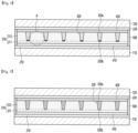
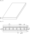
- a light route control member includes a first substrate 110, a second substrate 120, a first electrode 210, a second electrode 220, and a light conversion part 300.
- the first substrate 110 may support the first electrode 210.
- the first substrate 110 may be rigid or flexible.
- the first substrate 110 may be transparent.
- the first substrate 110 may include a transparent substrate capable of transmitting light.
- the first substrate 110 may include glass, plastic, or a flexible polymer film.
- the flexible polymer film may be made of any one of polyethylene terephthalate (PET), polycarbonate (PC), acrylonitrile-butadiene-styrene copolymer (ABS), polymethyl methacrylate (PMMA), polyethylene naphthalate (PEN), polyether sulfone (PES), cyclic olefin copolymer (COC), triacetylcellulose (TAC) film, polyvinyl alcohol (PVA) film, polyimide (PI) film, and polystyrene (PS), which is only an example, but the embodiment is not limited thereto.
- PET polyethylene terephthalate
- PC polycarbonate
- ABS acrylonitrile-butadiene-styrene copolymer
- PMMA polymethyl methacrylate
- PEN polyethylene naphthalate
- PES polyether sulfone
- COC cyclic
- the first substrate 110 may be a flexible substrate having flexible characteristics.
- the first substrate 110 may be a curved or bended substrate. That is, the light route control member including the first substrate 110 may also be formed to have flexible, curved, or bent characteristics. Accordingly, the light route control member according to the embodiment may be changed to various designs.
- the first electrode 210 is disposed on one surface of the first substrate 110.
- the first electrode 210 may be disposed on an upper surface of the first substrate 110. That is, the first electrode 210 is disposed between the first substrate 110 and the second substrate 120.
- the first electrode 210 may contain a transparent conductive material.
- the first electrode 210 may contain a metal oxide such as indium tin oxide, indium zinc oxide, copper oxide, tin oxide, zinc oxide, titanium oxide, etc.
- the first electrode 210 may be disposed on the first substrate 110 in a film shape.
- light transmittance of the first electrode 210 may be about 80% or more.
- the first electrode 210 may have a thickness of about 0.1um to about 0.5um.
- the first electrode 210 may contain various metals to realize low resistance.
- the first electrode 210 may contain at least one metal of chromium (Cr), nickel (Ni), copper (Cu), aluminum (Al), silver (Ag), molybdenum (Mo). gold (Au), titanium (Ti), and alloys thereof.
- the first electrode 210 may be disposed on the entire surface of one surface of the first substrate 110.
- the first electrode 210 may be disposed as a surface electrode on one surface of the first substrate 110.
- the embodiment is not limited thereto, and the first electrode 210 may be formed of a plurality of pattern electrodes having a predetermined pattern.
- the first electrode 210 may include a plurality of conductive patterns.
- the first electrode 210 may include a plurality of mesh lines intersecting each other and a plurality of mesh openings formed by the mesh lines.
- the first electrode 210 contains a metal, visibility may be improved because the first electrode is not visible from the outside.
- the light transmittance is increased by the openings, so that the brightness of the light route control member according to the embodiment may be improved.
- the second substrate 120 is disposed on the first substrate 110.
- the second substrate 120 may be disposed on the first electrode 210 on the first substrate 110.
- the second substrate 120 may contain a material capable of transmitting light.
- the second substrate 120 may contain a transparent material.
- the second substrate 120 may contain a material the same as or similar to that of the first substrate 110 described above.
- the second substrate 120 may include glass, plastic, or a flexible polymer film.
- the flexible polymer film may be made of any one of polyethylene terephthalate (PET), polycarbonate (PC), acrylonitrile-butadiene-styrene copolymer (ABS), polymethyl methacrylate (PMMA), polyethylene naphthalate (PEN), polyether sulfone (PES), cyclic olefin copolymer (COC), triacetylcellulose (TAC) film, polyvinyl alcohol (PVA) film, polyimide (PI) film, and polystyrene (PS), which is only an example, but the embodiment is not limited thereto.
- PET polyethylene terephthalate
- PC polycarbonate
- ABS acrylonitrile-butadiene-styrene copolymer
- PMMA polymethyl methacrylate
- PEN polyethylene naphthalate
- PES polyether sulfone
- COC cyclic
- the second substrate 120 may be a flexible substrate having flexible characteristics.
- the second substrate 120 may be a curved or bended substrate. That is, the light route control member including the second substrate 120 may also be formed to have flexible, curved, or bent characteristics. Accordingly, the light route control member according to the embodiment may be changed to various designs.
- the second substrate 120 may have a thickness of 30mm to 80mm.
- the second electrode 220 may be disposed on one surface of the second substrate 120.
- the second electrode 220 may be disposed on a lower surface of the second substrate 120. That is, the second electrode 220 may be disposed on a surface on which the second substrate 120 faces the first substrate 110. That is, the second electrode 220 may be disposed facing the first electrode 210 on the first substrate 110. That is, the second electrode 220 is disposed between the first electrode 210 and the second substrate 120.
- the second electrode 220 may contain a transparent conductive material.
- the second electrode 220 may contain a metal oxide such as indium tin oxide, indium zinc oxide, copper oxide, tin oxide, zinc oxide, titanium oxide, etc.
- the second electrode 220 may be disposed on the first substrate 110 in a film shape.
- the light transmittance of the second electrode 220 may be about 80% or more.
- the second electrode 220 may have a thickness of about 0.1um to about 0.5um.
- the second electrode 220 may contain various metals to realize low resistance.
- the second electrode 220 may contain at least one metal of chromium (Cr), nickel (Ni), copper (Cu), aluminum (Al), silver (Ag), molybdenum (Mo). gold (Au), titanium (Ti), and alloys thereof.
- the second electrode 220 may be disposed on the entire surface of one surface of the second substrate 120.
- the second electrode 220 may be disposed as a surface electrode on one surface of the second substrate 120.
- the embodiment is not limited thereto, and the second electrode 220 may be formed of a plurality of pattern electrodes having a predetermined pattern.
- the second electrode 220 may include a plurality of conductive patterns.
- the second electrode 220 may include a plurality of mesh lines intersecting each other and a plurality of mesh openings formed by the mesh lines.
- the second electrode 220 contains a metal
- visibility may be improved because the second electrode 220 is not visible from the outside.
- the light transmittance is increased by the openings, so that the brightness of the light route control member according to the embodiment may be improved.
- the light conversion part 300 is disposed between the first substrate 110 and the second substrate 120. In detail, the light conversion part 300 is disposed between the first electrode 210 and the second electrode 220.
- An adhesive layer 400 may be disposed at least one of between the light conversion part 300 and the first substrate 110 and between the light conversion part 300 and the second substrate 120, and the first substrate 110, the second substrate 120, and the light conversion part 300 may be adhered to each other by the adhesive layer 400.
- a buffer layer 410 for improving adhesion between the light conversion part 300 and the first electrode 210 is disposed between the light conversion part 300 and the first electrode 210, and the light conversion part 300 and the first electrode 210, which are different materials, may be easily bonded through the buffer layer 410.
- the light conversion part 300 includes a partition wall part 310 and a receiving part 320.
- the partition wall part 310 is defined as a partition wall region that partitions the receiving part. That is, the partition wall part 310 is a partition wall region partitioning a plurality of receiving parts. And the receiving part 320 is defined as a region that changes into a light blocking part and a light transmitting part according to the application of a voltage.
- the partition wall part 310 and the receiving part 320 are alternately disposed with each other.
- the partition wall part 310 and the receiving part 320 may be disposed to have different widths.
- the width of the partition wall portion 310 may be greater than the width of the receiving part 320.
- the partition wall part 310 and the receiving part 320 are alternately disposed with each other.
- the partition wall part 310 and the receiving part 320 are alternately disposed with each other. That is, each of the partition wall portions 310 is disposed between the receiving parts 320 adjacent to each other, and each of the receiving parts 320 is disposed between the adjacent partition wall portions 310.
- the partition wall part 310 may contain a transparent material.
- the partition wall part 310 may contain a material that may transmit light.
- the partition wall part 310 may contain a resin material.
- the partition wall part 310 may contain a photo-curable resin material.
- the partition wall part 310 may contain a UV resin or a transparent photoresist resin.
- the partition wall part 310 may contain urethane resin or acrylic resin.
- the partition wall part 310 may transmit light incident on any one of the first substrate 110 and the second substrate 120 toward another substrate.
- a light is emitted from the upper portion of the second substrate 120, and the light may pass through the light route control member to move downward of the first substrate 110.
- a sealing part 500 sealing the light route control member may be disposed on a side surface of the partition wall part, and a side surface of the light conversion part 300 may be sealed by the sealing part.
- the receiving part 320 includes a dispersion 320a and light conversion particles 320b. That is, a light conversion material including the dispersion 320a and the light conversion particles 320b are disposed inside the receiving part 320.
- the dispersion 320a is injected into the receiving part 320 and filled, and a plurality of light conversion particles 320b may be dispersed in the dispersion 320a.
- the dispersion 320a may be a material for dispersing the light conversion particles 320b.
- the dispersion 320a may contain a transparent material.
- the dispersion 320a may contain a non-polar solvent.
- the dispersion 320a may contain a material capable of transmitting light.
- the dispersion 320a may include at least one of a halocarbon-based oil, a paraffin-based oil, and isopropyl alcohol.
- the light conversion particles 320b may be disposed to be dispersed in the dispersion 330a.
- the plurality of light conversion particles 320b may be disposed to be spaced apart from each other in the dispersion 330a.
- the light conversion particles 320b may include a material capable of absorbing light. That is, the light conversion particle 320b may be a light absorbing particle.
- the light conversion particle 320b may have a color.
- the light conversion particles 320b may have a black-based color.
- the light conversion particles 320b may include carbon black particles.
- the surface of the light conversion particle 320b may be charged. Accordingly, according to the application of the voltage, the light conversion particles 320b may move in one direction.
- the light transmittance of the receiving part 320 is changed by the light conversion particles 320b.
- the receiving part 320 may be changed into a light blocking part and a light transmitting part by changing the light transmittance by the light conversion particles 320b. That is, the receiving part 320 changes the transmittance of the light passing through the receiving part 320 by dispersion and aggregation of the light conversion particles 320b disposed therein in the dispersion 320a.
- the light path member according to the claimed invention is able change from the first mode to the second mode or from the second mode to the first mode by a voltage applied to the first electrode 210 and the second electrode 220.
- the receiving part 320 becomes the light blocking part in the first mode, and light of a specific angle may be blocked by the receiving part 320. That is, a viewing angle of the user viewing from the outside may be narrowed.
- the receiving part 320 becomes the light transmitting part in the second mode, and in the light route control member according to the embodiment, light may be transmitted through both the partition wall part 310 and the receiving part 320. That is, the viewing angle of the user viewing from the outside may be widened.
- the light conversion particles 320b have electric charges on their surface, and may move in the direction of the first electrode 210 or the second electrode 220 by an applied voltage or by characteristics of the charge. That is, the light conversion particles 320b are, according to the claimed invention, electrophoretic particles.
- the receiving part 320 may be electrically connected to the first electrode 210 and the second electrode 220.
- the light conversion particles 320b of the receiving part 320 are uniformly dispersed in the dispersion 330a, and light may be blocked by the light conversion particles in the receiving part 320. Accordingly, in the first mode, the receiving part 320 may be driven as the light blocking part.
- the light conversion particles 320b may move.
- the light conversion particles 320b may move toward one end or the other end of the receiving part 320 by a voltage transmitted through the first electrode 210 and the second electrode 220. That is, the light conversion particles 320b may move from the receiving part 320 toward the first electrode or the second electrode.
- the light conversion particles 320b in a negatively charged state can be moved in the direction of the positively charged electrode among the first electrode 210 and the second electrode 220 using the dispersion 320a as a medium.
- the first electrode 210 and/or the second electrode 220 when a voltage is applied to the first electrode 210 and/or the second electrode 220, an electric field is formed between the first electrode 210 and the second electrode 220, and the charged carbon black, that is, the light conversion particles may be moved toward a positive electrode of the first electrode 210 and the second electrode 220 using the dispersion 320a as a medium.
- the light conversion particles 320b may be moved toward the first electrode 210 in the dispersion 330a. That is, the light conversion particles 320b are moved in one direction, and the receiving part 320 may be driven as the light transmitting part.
- the light conversion particles 320b may be uniformly dispersed in the dispersion 320a to drive the receiving part 30202 as the light blocking part.
- the light route control member according to the embodiment may be driven in two modes according to a user's surrounding environment. That is, when the user requires light transmission only at a specific viewing angle, the receiving unit is driven as the light blocking part, or in an environment in which the user requires high brightness, a voltage may be applied to drive the receiving unit as the light transmitting part.
- the light route control member according to the embodiment may be implemented in two modes according to the user's requirement, the light route control member may be applied regardless of the user's environment.
- the partition wall part 310 is formed to have a different density for each area of the partition wall part 310.
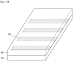
- the partition wall part 310 includes a base partition wall part 311 disposed on the first electrode 210 and a separation partition wall part 312 disposed on the base partition wall part 311.
- the partition wall part 310 includes a base partition wall part 311 disposed below the receiving part 320 and a separation partition wall part 312 disposed on the base partition wall part 311.
- the base partition wall part 311 and the separation partition wall part 312 may be formed to have different widths.
- the width of the base partition wall part 311 may be greater than the width of the separation partition wall part 312.
- the partition wall part 310 may be formed in a shape in which the width decreases while extending from the base partition wall part 311 to the separation partition wall part 312.
- the partition wall part 310 may have a dielectric characteristic to apply a voltage to the receiving part 320. Accordingly, since the base partition wall part 311 has dielectric properties, even when the receiving part 320 and the first electrode 210 disposed between the partition wall parts 310 are disposed to be spaced apart from each other, a voltage may be applied to the inside of the receiving part 320.
- the separation partition wall part 310 since the separation partition wall part 310 also has dielectric properties, there is a problem in that a current is leaked through the separation partition wall part 310 between the receiving parts 320, thereby increasing a driving voltage.
- the light route control member according to the claimed invention arranges a plurality of pores in the partition wall part 310, and the partition wall part is formed to have a different density for each region, the above problems can be solved.
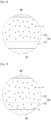
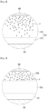
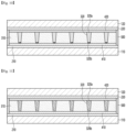
- FIGS. 6 to 9 are views illustrating enlarged views of partition wall parts according to various embodiments.
- a plurality of pores P are disposed in the partition wall part 310.
- the pores P are formed of an air layer formed inside the material forming the partition wall part in the partition wall part 310. That is, the pores P include air.
- the pores P may be disposed only in a specific region inside the partition wall part 310.
- the pores (P) are disposed only inside the separation partition wall part (312), and may not be disposed inside the base partition wall part 311.
- the partition wall part 310 Due to the pores P, the partition wall part 310 has a different density for each area.
- the density per unit area of the base partition wall part 311 is greater than the density per unit area of the separation partition wall part 312 due to the pores P.
- the density per unit area may be defined as the density per unit area of the partition wall part material. That is, by measuring the area of the partition wall part material in the unit area, the density per unit area of the partition wall part material in the base partition wall part 311 and the separation partition wall part 312 can be measured.
- the separation partition wall part 312 has a relatively reduced density per unit area due to the pores P disposed therein.
- the pores P may be disposed at a porosity of a certain size with respect to the entire separation partition wall part 312.
- the pores P may be disposed at a porosity of 0.5% to 50% with respect to the entire separation partition wall part 312.
- the pores P may be disposed at a porosity of 0.1% to 25% based on the entirety of the partition wall part 310.
- the light loss may increase due to scattering and refraction of light passing through the separation partition wall part 312 due to the pores of the separation partition wall part 312.
- the pores P disposed in the separation partition wall part 312 may reduce leakage of current from area between the receiving part in the direction of the separation partition wall part 312.
- the driving voltage of the light route control member is reduced, it is possible to drive the light route control member at a low voltage, thereby improving the driving characteristics.
- the support force of the partition wall part may be secured.
- a plurality of pores P are disposed in the partition wall part 310.
- the pores P are formed of an air layer formed inside the material forming the partition wall part in the partition wall part 310. That is, the pores P include air.
- the pores P may be arranged in different volumes for each area within the partition wall part 310.
- the pores P may be disposed in both the base partition wall part 311 and the separation partition wall part 312.
- a volume per unit area of the pores P of the base partition wall part 311 and a volume per unit area of the pores P of the separation partition wall part 312 may be different from each other.
- the volume per unit area of the pores P of the base partition wall part 311 may be smaller than the volume per unit area of the pores P of the separation partition wall part 312.
- the pores P may be disposed relatively more in the separation partition wall part 312 than in the base partition wall part 311.
- the amount of the pores P may be controlled when forming the partition wall part 310.
- pores formed during the filling process are artificially removed before releasing the mold. Accordingly, the pores P inside the partition wall part can be arranged differently for each region.
- the pores P of the base partition wall part 311 may be remain by a certain volume.
- the pores P may remain within a range capable of maintaining the supporting force of the base partition wall part 311.
- the separation partition wall part 312 has a relatively reduced density per unit area due to the pores P disposed therein.
- the pores P may be disposed at a porosity of a certain size with respect to the entire separation partition wall part 312.
- the pores P may be disposed at a porosity of 0.5% to 50% with respect to the entire separation partition wall part 312.
- the pores P may be disposed at a porosity of 0.1% to 25% based on the entirety of the partition wall part 310.
- the light loss may increase due to scattering and refraction of light passing through the separation partition wall part 312 due to the pores of the separation partition wall part 312.
- the pores P disposed in the separation partition wall part 312 may reduce current leakage between the receiving parts in the direction of the separation partition wall part 312 when the light route control member is driven.
- a plurality of pores P are disposed in the partition wall part 310.
- the pores P are formed of an air layer formed inside the material forming the partition wall part in the partition wall part 310. That is, the pores P include air.
- the pores P may be disposed only in a specific region inside the partition wall part 310.
- the pores P may be disposed only inside the separation partition wall part 312, and may not be disposed inside the base partition wall part 311.
- the partition wall part 310 Due to the pores P, the partition wall part 310 has a different density for each area. In detail, the density per unit area of the base partition wall part 311 is greater than the density per unit area of the separation partition wall part 312 due to the pores P.
- the separation partition wall part 312 has a relatively reduced density per unit area due to the pores P disposed therein.
- the pores P may be disposed at a porosity of a certain size with respect to the entire separation partition wall part 312.
- the pores P may be disposed at a porosity of 0.5% to 50% with respect to the entire separation partition wall part 312.
- the dielectric properties of the separation partition wall part 312 are not sufficiently reduced. Accordingly, a leakage current may be increased in a direction from the receiving part to the separation partition wall part.
- a light loss may increase because scattering and refraction of light passing through the separation partition wall part 312 may occur due to the pores of the separation partition wall part 312.
- the pores P are disposed in different amounts for each area in the separation partition wall part 312. That is, the pores P are arranged in different volumes for each area in the separation partition wall part 312.
- the amount of the pores P that is, the volume of the pores P decreases while extending in the direction of the base partition wall part 311 inside the separation partition wall part 312.
- the amount of the pores P that is, the volume of the pores P decreases while extending in a direction in which the light moves. That is, the amount of the pores P, that is, the volume of the pores P, decreases while extending in the movement direction of the light.
- the pores P disposed in the separation partition wall part 312 may reduce current leakage between the receiving parts in the direction of the separation partition wall part 312 when the light route control member is driven.
- the support force of the partition wall part may be secured.
- the amount of the pores (P), that is, the volume of the pores (P) is arranged differently for each area inside the partition wall part. Accordingly, it is possible to minimize the scattering of the light emitted toward the user. That is, the amount of the pores (P), that is, the volume of the pores (P) based on the movement direction of the light decreases while extending in the movement direction of the light. Accordingly, it is possible to minimize scattering of light moving in the user direction, thereby improving the frontal luminance of the light.
- a clearer display may be viewed by the improved front luminance.
- pores are not disposed in the base partition wall part, but the embodiment is not limited, and pores maintaining the strength of the partition wall part may be included in the partition wall part as shown in FIG 7 .
- a plurality of pores P may be disposed in the partition wall part 310.
- the pores P are formed of an air layer formed inside the material forming the partition wall part in the partition wall part 310. That is, the pores P include air.
- the pores P may be disposed only in a specific region inside the partition wall part 310.
- the pores P may be disposed only inside the separation partition wall part 312, and may not be disposed inside the base partition wall part 311.
- the partition wall part 310 may have a different density for each area.
- the density per unit area of the base partition wall part 311 may be greater than the density per unit area of the separation partition wall part 312 due to the pores P.
- the separation partition wall part 312 may have a relatively reduced density per unit area due to the pores P disposed therein.
- the pores P may be disposed at a porosity of a certain size with respect to the entire separation partition wall part 312.
- the pores P may be disposed at a porosity of 0.5% to 50% with respect to the entire separation partition wall part 312.
- the pores P may be disposed at a porosity of 0.1% to 25% based on the entirety of the partition wall part 310.
- the dielectric properties of the separation partition wall part 312 are not sufficiently reduced. Accordingly, a leakage current may be increased in a direction from the receiving part to the separation partition wall part.
- a light loss may increase due to scattering and refraction of light passing through the separation partition wall part 312 due to the pores of the partition wall part 312.
- the pores P may be disposed in a partial area inside the separation partition wall part 312. In detail, the pores P may be disposed only in the direction of the second substrate 120 inside the separation partition wall part 312.
- the separation partition wall part 312 may be defined a first separation partition wall part 312a in a direction close to the first substrate 110 and a second separation partition wall part 312b in a direction close to the second substrate 120, and the pores P may be disposed only in the second separation partition wall part 312b.
- the pores P may be disposed only in the second separation partition wall part 312b close to an exit portion of the light emitted from the display panel.
- the first separation partition wall part 312a and the second separation partition wall part 312b may be disposed to have different thicknesses.
- the thickness of the second separation partition wall part 312b may be less than or equal to the thickness of the first separation partition wall part 312a.
- the second separation partition wall part 312b may have a thickness of 20% to 50% of the total thickness of the separation partition wall part.
- the pores P disposed in the separation partition wall part 312 may reduce current leakage between the receiving parts in the direction of the separation partition wall part 312 when the light route control member is driven.
- the support force of the partition wall part may be secured.
- the pores P are disposed only in a direction close to the light exit portion and not in a direction close to the light incidence portion, scattering of light emitted from the incidence portion toward the user may be minimized. That is, by arranging the pores P only on the exit portion part based on the movement direction of light, scattering of light from the incidence portion can be minimized and the frontal luminance of the light can be improved from the incident portion.
- a clearer display may be viewed by the improved front luminance.
- the base partition wall part may include pores sufficient to maintain the strength of the partition wall part.
- the partition wall part of the light route control member according to the embodiment may have different densities per unit area of the partition wall material of the separation partition wall part and the base partition wall part.
- a plurality of pores is disposed inside the partition wall part, and the densities per unit area of the separation partition wall part and the base partition wall part may be different by the pores.
- the driving characteristics, visibility, and reliability of the light route control member may be improved by varying the porosity of the base partition wall part supporting the separation partition wall part and the separation partition wall part dividing the receiving part into a plurality of receiving parts.
- the porosity is relatively increased in the separation partition wall part disposed between the receiving parts compared to the base partition wall part, and leakage current to the separation partition wall part between the receiving parts can be minimized due to the dielectric properties of the partition wall part.
- the base partition wall part may not include pores or have a reduced porosity. Accordingly, the strength of the base partition wall part can be secured. Accordingly, the reliability of the light route control member can be improved by stably supporting the separation partition wall part by the base partition wall part.
- the pores disposed inside the separation partition wall part may be different for each region, that is, the porosity of the light emitting part may be increased more than the porosity of the light incident part. Accordingly, when light is emitted in the direction of the user, scattering and refraction by the pores can be prevented.
- FIGS. 10 to 13 are views illustrating other cross-sectional views of a light route control member according to an embodiment which is not according to the claimed invention.
- the receiving part 320 may be disposed in contact with the electrode differently from FIGS. 4 to 7 .
- the receiving part 320 may be disposed in direct contact with the first electrode 210.
- the first electrode 210 and the receiving part 320 are not spaced apart and are arranged in direct contact with each other, the voltage applied from the first electrode 210 may be easily transferred to the receiving part 320.
- the receiving part 320 may be disposed while having a constant inclination angle ⁇ .
- the receiving part 320 may be disposed with an inclination angle ⁇ of greater than 0° to less than 90° with respect to the first electrode 210.
- the receiving part 320 may extend upwardly while having an inclination angle ⁇ of greater than 0° to less than 90° with respect to one surface of the first electrode 210.
- the first electrode 210 may be disposed inside the light conversion part 300.
- the first electrode 210 may be disposed to be embedded in the light conversion part disposed on the first substrate 110.
- the first electrode 210 may include a plurality of electrode parts, and each electrode part may be disposed inside each receiving part 320.
- the first electrode 210 may be disposed inside the receiving part 320 and extend in the same direction as the extending direction of the receiving part 320.
- the receiving part 320 may be in direct contact with the first electrode 210. That is, the dispersion 320a in which the light conversion particles 320b disposed inside the receiving part 320 are dispersed may be in direct contact with the first electrode 210.
- the first electrode 210 may be formed of a metal paste including conductive particles.
- the first electrode 210 may be formed by filling and curing the metal paste inside the receiving part 320.
- the metal paste forming the first electrode 210 may include conductive particles and an organic material.
- the conductive particles may include a metal.
- the conductive particles may include silver particles.
- the conductive particles may be formed in a spherical shape.
- the conductive particles may have a particle diameter of 1 ⁇ m or less.
- the particle diameter of the conductive particles may be in the range of 0.05 ⁇ m to 1 ⁇ m.
- the particle diameter of the conductive particles is less than 0.05 ⁇ m, a shape in which the conductive particles are aggregated in the binder may occur.
- the particle diameter of the conductive particles exceeds 1 ⁇ m, filling characteristics may be reduced when the metal paste is filled into the receiving part.
- the particle diameter of the conductive particles may be less than or equal to the width w of the receiving part.
- the width w of the receiving part may be defined as a long width among the widths of the receiving part having a long width and a short width.
- the particle diameter of the conductive particles may be 0.01 times to 0.2 times the size of the width w of the receiving part.
- the particle diameter of the conductive particles is less than 0.01 times the width w of the receiving part, when the metal paste is filled into the receiving part, since the size of the conductive particles is too small, the conductive particles may adhere to the inner surface of the receiving part while moving to the bottom surface of the receiving part. As a result, the number of conductive particles in the first electrode disposed on the bottom surface of the receiving part may be reduced, so that conductivity may be reduced.
- the particle diameter of the conductive particles exceeds 0.2 times the width w of the receiving part
- the conductive particles may be fixed in the middle of the receiving part without moving to the bottom surface of the receiving part.
- the number of conductive particles in the first electrode disposed on the bottom surface of the receiving part may be reduced, so that conductivity may be reduced.
- the conductive particles and the organic material may be included in a constant weight %, respectively.
- the organic material may include a binder, a curing agent, and other additives.
- the conductive particles may be included in an amount of about 60 wt% to about 85 wt% based on the total weight of the metal paste.
- the conductivity of the first electrode formed by the metal paste may be reduced.
- the viscosity of the metal paste may increase, and thus, when the metal paste is filled into the receiving part, the filling characteristics may be reduced.
- the binder and the organic material of the additive may be included in an amount of about 15 wt% to about 40 wt% based on the total weight of the metal paste.
- the binder may be included in an amount of 40% to 50% by weight based on the entire organic material
- the curing agent may be included in an amount of 30% to 40% by weight based on the entire organic material
- the additive may be included in an amount of 10% to 30% by weight based on the entire organic material.
- the binder is a main material for forming the adhesive force of the first electrode formed by the metal paste, and may include a polymer material such as epoxy, ethyl cellulose, or acrylate.
- the curing agent is included to cure the metal paste, and may include at least one of an Acid anhydride, an Amine, a Phenol, and a Thiol as a polymer for curing.
- the additive may include a dispersing agent for dispersing the metal paste and a thixotropic additive for imparting thixotropic properties.
- the first electrode 210 may include a plurality of pores.
- a plurality of pores may be formed in the first electrode 210 formed by curing the metal paste.
- the porosity of the first electrode 210 may be 5% to 45%. Making the porosity of the first electrode 210 less than 5% may be difficult to implement in the process. In addition, when the porosity of the first electrode 210 exceeds 45%, the dispersion or light conversion particles inside the receiving part may penetrate between the pores, and the adhesion of the first electrode 210 may be reduced.
- the porosity of the first electrode 210 is satisfied in the range of 5% to 45%, the interface specific surface area of the first electrode 210 and the dispersion disposed on the first electrode 210 is increased to increase the electric field can be efficiently formed, and the driving characteristics of the light route control member can be improved.
- the metal paste forming the first electrode 210 may include conductive particles having different particle diameters to satisfy the porosity of the first electrode 210.
- the metal paste may include first conductive particles having a particle diameter of 0.5 ⁇ m to 1.5 ⁇ m and second conductive particles having a particle diameter of 6.5 ⁇ m to 7.5 ⁇ m, and the first conductive particles may be included in an amount of 25 wt% to 35 wt% with respect to the entire conductive particle, and the second conductive particle may be included in an amount of 65 wt% to 75 wt% based on the entire conductive particle.
- the porosity of the first electrode 210 formed by the metal paste by the first and second conductive particles included in different particle sizes and in different amounts as described above is realized to be 5% to 45%. Accordingly, adhesive properties and driving properties can be improved.
- the first electrode 210 may be formed to have a thickness smaller than a thickness T of the receiving part 320 inside the receiving part 320.
- the thickness t1 of the first electrode 210 may be defined as the minimum thickness of the first electrode 210.
- the thickness t1 of the first electrode 210 may have a minimum thickness and a maximum thickness.
- the thickness t1 of the first electrode 210 described below may be defined as the minimum thickness of the first electrode 210 that is the center of the convex surface of the first electrode 210.
- the thickness t1 of the first electrode 210 may be 5% to 20% of the thickness T of the receiving part 320.
- the thickness t1 of the first electrode 210 may be 5 ⁇ m to 20 ⁇ m.
- the conductivity of the first electrode 210 may be reduced, and thus driving characteristics of the light route control member may be reduced.
- the thickness t1 of the first electrode 210 exceeds 20% of the thickness T of the receiving part 320, when the light route control member passes through the light conversion unit 300, the movement of light is prevented by the first electrode 210, so that the light transmittance of the light route control member in the second mode may be reduced.
- the thickness t1 of the first electrode 210 may be related to the width w of the receiving part 320.
- the aspect ratio between the thickness t1 of the first electrode 210 and the width w of the receiving part 320 may be 1.1 to 1.4.
- the conductivity of the first electrode 210 is secured, it is possible to improve the driving characteristics of the light route control member, and to minimize the interference of the movement of light by the first electrode 210 to secure the light transmittance of the light route control member in the second mode.
- the first electrodes 210 disposed in the respective receiving parts may have the same or similar thickness to each other.
- the thickness difference between the plurality of first electrodes 210 disposed in each of the receiving parts may be 5% to 30% of the average thickness of the first electrodes 210. It is difficult to implement in a process that the thickness difference of the plurality of first electrodes 210 is less than 5% of the average thickness of the first electrodes 210, and when the thickness difference of the plurality of first electrodes 210 exceeds 30% of the average thickness of the first electrodes 210, due to a difference in the thickness of the first electrode disposed in each receiving part, conductivity in each receiving part is different. Accordingly, the overall driving characteristics of the light route control member may be reduced due to a difference in driving speed of each receiving part.
- the first electrode for applying a voltage to the receiving part may be disposed inside the receiving part rather than outside the receiving part.
- the dispersion in which the light conversion particles are dispersed in the receiving part may be disposed in direct contact with the first electrode. Accordingly, since the distance difference between the dispersion and the first electrode is eliminated, the voltage applied from the first electrode is directly transferred to the dispersion, thereby improving the driving speed of the light route control member.
- the first electrode is disposed outside the receiving part, and accordingly, the dispersion in the receiving part and the first electrode are disposed to be spaced apart by the thickness of the base partition wall part.
- the base partition wall part has a dielectric characteristic of a certain size, there is a limitation in the selection of materials for the partition wall part. Also, when the thickness of the base partition wall part increases, the movement speed of the voltage applied from the first electrode to the receiving part is reduced, and thus the thickness of the base partition wall part is limited.
- the difference in the distance between the dispersion and the first electrode may be eliminated by patterning and disposing the first electrode inside the receiving part. Thereby, the driving speed of the light route control member can be improved.
- the material of the partition wall part can be freely selected.
- the thickness of the base partition wall part it is possible to secure the support force of the partition wall part. Thereby, the reliability of the light route control member can be improved.
- the thickness t2 of the base partition wall part 311 may be about 5 ⁇ m to 35 ⁇ m. Accordingly, since it is possible to form the thickness t2 of the base partition wall part 311 to a thickness greater than that of the prior art, the strength of the base partition wall part 311 can be improved, thereby improving the supporting force of the partition wall part.
- the composition and composition ratio of the metal paste forming the first electrode and the particle diameter of the conductive particles it is possible to secure the filling and adhesion properties of the first electrode, and by making the thicknesses of the plurality of first electrodes disposed in the plurality of receiving parts uniform, a difference in driving speed of each receiving part may be minimized, and driving characteristics of the light route control member may be improved.
- the partition wall part including a resin material is bonded to a substrate including a resin material rather than an electrode including a metal material, that is, the first partition wall part, which is the light conversion part or the base partition wall part, is in direct contact with the first substrate. Therefore, it is possible to improve the adhesion between the light conversion part and the substrate.
- FIGS. 19 to 23 a display device and a display apparatus to which the light route control member according to an embodiment is applied will be described.
- the light route control member 1000 may be disposed on or under display panel 2000.
- the display panel 2000 and the light route control member 1000 may be disposed to be adhered to each other.
- the display panel 2000 and the light route control member 1000 may be adhered to each other via an adhesive layer 1500.
- the adhesive layer 1500 may be transparent.
- the adhesive layer 1500 may include an adhesive or an adhesive layer containing an optical transparent adhesive material.
- the adhesive layer 1500 may include a release film.
- the light route control member and the display panel may be adhered after the release film is removed.
- one end or one end and the other end of the light route control member may protrude, and the light conversion part may not be disposed on the protruding portion.
- the protrusion region is an electrode connection portion, and may connect an external printed circuit board and the light route control member through the electrode connection portion.
- the display panel 2000 may include a first substrate 2100 and a second substrate 2200.
- the light route control member may be formed under the liquid crystal panel. That is, when the user-viewed side of the liquid crystal panel is defined as the upper portion of the liquid crystal panel, the light route control member may be disposed under the liquid crystal panel.
- the display panel 2000 may be formed in a structure in which the first substrate 2100 including a thin film transistor (TFT) and a pixel electrode and the second substrate 2200 including color filter layers are bonded with a liquid crystal layer interposed therebetween.
- TFT thin film transistor
- the display panel 2000 may be a liquid crystal display panel of a color filter on transistor (COT) structure in which a thin film transistor, a color filter, and a black matrix are formed at the first substrate 2100 and the second substrate 2200 is bonded to the first substrate 2100 with the liquid crystal layer interposed therebetween. That is, a thin film transistor may be formed on the first substrate 2100, a protective film may be formed on the thin film transistor, and a color filter layer may be formed on the protective film. In addition, a pixel electrode in contact with the thin film transistor may be formed on the first substrate 2100. At this point, in order to improve an aperture ratio and simplify a masking process, the black matrix may be omitted, and a common electrode may be formed to function as the black matrix.
- COT color filter on transistor
- the display device may further include a backlight unit providing light from a rear surface of the display panel 2000.
- the light route control member is disposed below the liquid crystal panel and above the backlight unit 3000, and the light route control member may be disposed between the backlight unit 3000 and the display panel 2000.
- the light route control member may be formed on the organic light emitting diode panel. That is, when the surface viewed by the user of the organic light emitting diode panel is defined as the upper portion of the organic light emitting diode panel, the light route control member may be disposed on the organic light emitting diode panel.
- the display panel 2000 may include a self-luminous element that does not require a separate light source.
- a thin film transistor may be formed on the first substrate 2100, and an organic light emitting element in contact with the thin film transistor may be formed.
- the organic light emitting element may include an anode, a cathode, and an organic light emitting layer formed between the anode and the cathode. Further, the second substrate 2200 configured to function as an encapsulation substrate for encapsulation may further be included on the organic light emitting element.
- the light emitted from the display panel 2000 or the backlight unit 3000 may move from the second substrate 120 of the light route control member to the first substrate 110.
- a polarizing plate may be further disposed between the light route control member 1000 and the display panel 2000.
- the polarizing plate may be a linear polarizing plate or an external light reflection preventive polarizing plate.
- the polarizing plate may be the linear polarizing plate.
- the polarizing plate may be the external light reflection preventive polarizing plate.
- an additional functional layer 1300 such as an anti-reflection layer, an anti-glare, or the like may be further disposed on the light route control member 1000.
- the functional layer 1300 may be adhered to one surface of first substrate 110 of the light route control member.
- the functional layer 1300 may be adhered to the first substrate 110 of the light route control member via an adhesive layer.
- a release film for protecting the functional layer may be further disposed on the functional layer 1300.
- a touch panel may be further disposed between the display panel and the light route control member.
- the light route control member is disposed at an upper portion of the display panel, but the embodiment is not limited thereto, and the light route control member may be disposed at various positions such as a position in which light is adjustable, that is, a lower portion of the display panel, between a second substrate and a first substrate of the display panel, or the like.
- the light conversion part of the light route control member according to the embodiment is shown in a direction parallel or perpendicular to the outer surface of the second substrate, but the light conversion part may be formed to be inclined at a predetermined angle from the outer surface of the second substrate. Accordingly, a moire phenomenon occurring between the display panel and the light route control member may be reduced.
- the light route control member according to the embodiment may be applied to various display devices.
- the light route control member according to the embodiment may be applied to a display device that displays a display.
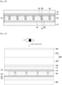
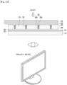
- the receiving unit when power is not applied to the light route control member as shown in FIG. 21 , the receiving unit functions as the light blocking part, so that the display device is driven in a light blocking mode, and when power is applied to the light route control member as shown in FIG. 22 , the receiving unit functions as the light transmitting part, so that the display device may be driven in an open mode.
- a user may easily drive the display device in a privacy mode or a normal mode according to application of power.
- the light emitted from the backlight unit or the self-luminous device may move from the first substrate to the second substrate.
- the light emitted from the backlight unit or the self-luminous device may also move from the second substrate to the first substrate.
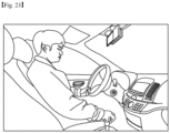
- the display device to which the light route control member according to the embodiment is applied may also be applied inside the vehicle.
- the display device including the light route control member may display a video confirming information of the vehicle and a movement route of the vehicle.
- the display device may be disposed between a driver seat and a passenger seat of the vehicle.
- the light route control member according to the embodiment may be applied to a dashboard that displays a speed, an engine, an alarm signal, and the like of the vehicle.
- the light route control member according to the embodiment may be applied to a front glass (FG) of the vehicle or right and left window glasses.
Landscapes
- Physics & Mathematics (AREA)
- Nonlinear Science (AREA)
- General Physics & Mathematics (AREA)
- Optics & Photonics (AREA)
- Chemical & Material Sciences (AREA)
- Crystallography & Structural Chemistry (AREA)
- Health & Medical Sciences (AREA)
- Life Sciences & Earth Sciences (AREA)
- Chemical Kinetics & Catalysis (AREA)
- Electrochemistry (AREA)
- Molecular Biology (AREA)
- Mathematical Physics (AREA)
- Electrochromic Elements, Electrophoresis, Or Variable Reflection Or Absorption Elements (AREA)
Claims (9)
- Élément de commande de trajet optique (1000) comprenant :un premier substrat (110) ;une première électrode (210) disposée sur le premier substrat (110) ;un second substrat (120) disposé sur le premier substrat (110) ;une seconde électrode (220) disposée sous le second substrat (120) ; et une partie de modification de la lumière (300) disposée entre la première électrode et la secondeélectrode et adaptée pour modifier l'angle de vision de la lumière transmise par l'élément de commande de trajet de la lumière en fonction d'un mouvement de particules électrophorétiques,dans lequel la partie de modification de la lumière (300) inclut une partie de paroi de séparation (310) et une partie réceptrice (320) qui sont disposées en alternance,dans lequel la transmission de la lumière de la partie réceptrice comprenant les particules électrophorétiques est modifiée en fonction de l'application d'une tension à la première et à la seconde électrodes,dans lequel la partie de paroi de séparation (310) inclut une partie partie de paroi de séparation de base (311)disposée sur la première électrode (210) en dessous de la partie réceptrice (320) et une partie de paroi de séparation (312) disposée sur la partie de paroi de séparation de base (311)dans lequel l'élément de commande de trajet optique (1000) est adapté pour passer d'un premier mode à un second mode, un angle de vision défini par la lumière transmise à travers l'élément de commande de trajet optique étant plus étroit dans le premier mode que dans le second,dans lequel une pluralité de pores (P) est disposée dans la partie de paroi de séparation (311) et éventuellement dans la partie de paroi de séparation de base (312),dans lequel les pores (P) incluent de l'air,dans lequel, grâce aux pores,une densité par unité de surface du matériau de la paroi de séparation (312) est inférieure à la densité par unité de surface du matériau de la paroi de séparation de la partie de paroi de séparation de base (311), etdans lequel le volume des pores (P) diminue en s'étendant de la partie de paroi de séparation (312) à la partie de la paroi de séparation de base (311) à l'intérieur de la partie de la paroi de séparation (312).
- Élément de commande de trajet optique (1000) selon la revendication 1, dans lequel la lumière est émise par une source lumineuse et est transmise au premier substrat (110) et au second substrat (120),
dans lequel la lumière se déplace du second substrat (120) vers le premier substrat (110). - Élément de commande de trajet optique (1000) selon la revendication 1 ou 2, dans lequel les pores (P) sont uniquement disposés dans la partie de paroi de séparation (312).
- Élément de commande de trajet optique (1000) selon la revendication 3, dans lequel les pores (P) sont disposés à une porosité de 0,5 % à 50 % par rapport au volume total de la partie de paroi de séparation (312).
- Élément de commande de trajet optique (1000) selon la revendication 3, dans lequel les pores (P) sont disposés à une porosité de 0,1 % à 25 % par rapport au volume total de la partie de paroi de séparation (310).
- Élément de commande de trajet optique (1000) selon l'une quelconque des revendications 1 à 5, dans lequel les pores (P) sont disposés dans la partie de paroi de séparation de base (311) et la partie de paroi de séparation (312).
dans lequel un volume par unité de surface des pores (P) de la paroi de séparation de base (311) est inférieur à un volume par unité de surface des pores (P) de la paroi de séparation (312). - Élément de commande de trajet optique (1000) selon l'une quelconque des revendications 1 à 6, dans lequel la partie de paroi de séparation (312) comprend une première paroi de séparation (312a) dans une direction proche du premier substrat (110) et une seconde partie de la paroi de séparation (312b) dans une direction proche du second substrat (120),
dans lequel les pores (P) sont disposés uniquement dans la seconde partie de paroi de séparation (312b). - Élément de commande de trajet optique (1000) selon la revendication 7, dans lequel la seconde partie de paroi de séparation (312b) a une épaisseur comprise entre 20 % et 50 % de l'épaisseur totale de la partie de paroi de séparation (312).
- Dispositif d'affichage comprenant :un panneau d'affichage (2000) ; etun élément de commande de trajet optique (1000) selon l'une quelconque des revendications 1 à 12 disposé sur le panneau de commande (2000).
Applications Claiming Priority (3)
| Application Number | Priority Date | Filing Date | Title |
|---|---|---|---|
| KR1020200004865A KR102756135B1 (ko) | 2020-01-14 | 2020-01-14 | 광 경로 제어 부재 및 이를 포함하는 디스플레이 장치 |
| KR1020200004829A KR102783586B1 (ko) | 2020-01-14 | 2020-01-14 | 광 경로 제어 부재 및 이를 포함하는 디스플레이 장치 |
| PCT/KR2021/000332 WO2021145619A1 (fr) | 2020-01-14 | 2021-01-11 | Élément de commande de trajet optique et dispositif d'affichage le comprenant |
Publications (3)
| Publication Number | Publication Date |
|---|---|
| EP4092480A1 EP4092480A1 (fr) | 2022-11-23 |
| EP4092480A4 EP4092480A4 (fr) | 2024-01-24 |
| EP4092480B1 true EP4092480B1 (fr) | 2025-06-11 |
Family
ID=76864518
Family Applications (1)
| Application Number | Title | Priority Date | Filing Date |
|---|---|---|---|
| EP21740854.1A Active EP4092480B1 (fr) | 2020-01-14 | 2021-01-11 | Élément de commande de trajet optique et dispositif d'affichage le comprenant |
Country Status (5)
| Country | Link |
|---|---|
| US (1) | US12345997B2 (fr) |
| EP (1) | EP4092480B1 (fr) |
| JP (1) | JP2023510295A (fr) |
| CN (1) | CN114945864A (fr) |
| WO (1) | WO2021145619A1 (fr) |
Families Citing this family (2)
| Publication number | Priority date | Publication date | Assignee | Title |
|---|---|---|---|---|
| JP7796459B2 (ja) * | 2022-07-22 | 2026-01-09 | パナソニックオートモーティブシステムズ株式会社 | カバーパネル及びディスプレイ装置 |
| CN117555177B (zh) * | 2023-12-07 | 2025-10-03 | 惠科股份有限公司 | 背光模组、导光组件和显示装置 |
Family Cites Families (21)
| Publication number | Priority date | Publication date | Assignee | Title |
|---|---|---|---|---|
| JPH11185630A (ja) * | 1997-12-22 | 1999-07-09 | Kyocera Corp | プラズマディスプレイパネル |
| CN101341440A (zh) * | 2005-12-20 | 2009-01-07 | 皇家飞利浦电子股份有限公司 | 改进型面内切换电泳显示器 |
| KR20080090852A (ko) | 2007-04-06 | 2008-10-09 | 엘지마이크론 주식회사 | 다공성 격벽을 구비한 평판형 램프 |
| KR100843552B1 (ko) | 2007-07-19 | 2008-07-04 | 한국전자통신연구원 | 나노 임프린트 공정을 이용한 나노 전극선 제조 방법 |
| KR101649290B1 (ko) | 2009-02-11 | 2016-08-31 | 삼성전자 주식회사 | 전기변색 소자 및 그 제조 방법 |
| JP2010191125A (ja) | 2009-02-18 | 2010-09-02 | Bridgestone Corp | 情報表示パネル用パターン電極の製造方法、及び情報表示パネル |
| KR20110028952A (ko) | 2009-09-14 | 2011-03-22 | 삼성전기주식회사 | 전자 종이 표시장치 및 그 제조방법 |
| KR20110139943A (ko) | 2010-06-24 | 2011-12-30 | 삼성전기주식회사 | 전자종이 표시소자 및 그 제조방법 |
| KR101687720B1 (ko) * | 2010-07-14 | 2016-12-29 | 엘지디스플레이 주식회사 | 전기영동 표시소자 및 그 제조방법 |
| KR101719158B1 (ko) | 2010-07-22 | 2017-03-23 | 엘지디스플레이 주식회사 | 전기영동 표시장치 및 그 제조방법 |
| KR101241306B1 (ko) * | 2010-07-29 | 2013-03-11 | 주식회사 이미지앤머터리얼스 | 윈도우 필터 시트 및 이를 이용한 윈도우 조립체 |
| JP2013033125A (ja) | 2011-08-02 | 2013-02-14 | Seiko Epson Corp | 電気泳動表示シート、電気泳動表示装置及びその製造方法、並びに電子機器 |
| KR101989495B1 (ko) * | 2012-04-04 | 2019-06-14 | 엘지디스플레이 주식회사 | 전기영동 표시장치와 그 제조방법 |
| JP5895677B2 (ja) | 2012-04-10 | 2016-03-30 | セイコーエプソン株式会社 | 表示シート、表示シートの製造方法、表示装置および電子機器 |
| KR101756506B1 (ko) | 2014-04-29 | 2017-07-11 | (주)엘지하우시스 | 광 투과율 가변 필름 및 이를 포함한 표시 장치 |
| KR101971874B1 (ko) | 2015-02-04 | 2019-04-25 | (주)엘지하우시스 | 광투과율 가변 필름, 이를 포함한 표시 장치 및 광투과율 가변 필름의 제조 방법 |
| US9911824B2 (en) * | 2015-09-18 | 2018-03-06 | Taiwan Semiconductor Manufacturing Co., Ltd. | Semiconductor structure with multi spacer |
| KR20180004879A (ko) * | 2016-07-04 | 2018-01-15 | 삼성디스플레이 주식회사 | 표시 장치 |
| KR102374549B1 (ko) | 2017-05-16 | 2022-03-14 | 엘지디스플레이 주식회사 | 광 제어장치 및 그를 포함한 투명표시장치 |
| JP2019070732A (ja) | 2017-10-10 | 2019-05-09 | セイコーエプソン株式会社 | 電気泳動装置及び電子機器 |
| CN109904120B (zh) * | 2017-12-11 | 2021-12-14 | 中芯国际集成电路制造(北京)有限公司 | 半导体器件及其制造方法 |
-
2021
- 2021-01-11 CN CN202180009187.XA patent/CN114945864A/zh active Pending
- 2021-01-11 US US17/758,854 patent/US12345997B2/en active Active
- 2021-01-11 EP EP21740854.1A patent/EP4092480B1/fr active Active
- 2021-01-11 JP JP2022542059A patent/JP2023510295A/ja active Pending
- 2021-01-11 WO PCT/KR2021/000332 patent/WO2021145619A1/fr not_active Ceased
Also Published As
| Publication number | Publication date |
|---|---|
| CN114945864A (zh) | 2022-08-26 |
| US20230040154A1 (en) | 2023-02-09 |
| EP4092480A4 (fr) | 2024-01-24 |
| WO2021145619A1 (fr) | 2021-07-22 |
| EP4092480A1 (fr) | 2022-11-23 |
| US12345997B2 (en) | 2025-07-01 |
| JP2023510295A (ja) | 2023-03-13 |
Similar Documents
| Publication | Publication Date | Title |
|---|---|---|
| EP4174566B1 (fr) | Élément de commande de trajet optique et dispositif d'affichage le comprenant | |
| US12372845B2 (en) | Optical path control member and display device comprising same | |
| EP4006620A1 (fr) | Élément de commande de trajet optique et dispositif d'affichage le comprenant | |
| EP4174565B1 (fr) | Élément de commande de trajet optique et dispositif d'affichage le comprenant | |
| US12019319B2 (en) | Optical path control member and display device comprising same | |
| EP4092480B1 (fr) | Élément de commande de trajet optique et dispositif d'affichage le comprenant | |
| US12007643B2 (en) | Optical path control member and display device comprising same | |
| US12111533B2 (en) | Light route control member and display device having the same | |
| US12242091B2 (en) | Optical path control member and display device comprising same | |
| KR102756135B1 (ko) | 광 경로 제어 부재 및 이를 포함하는 디스플레이 장치 | |
| US12523912B2 (en) | Light route control member and display device comprising same | |
| KR102783586B1 (ko) | 광 경로 제어 부재 및 이를 포함하는 디스플레이 장치 | |
| US20250199372A1 (en) | Optical path control member and display device comprising same | |
| US20250093733A1 (en) | Light path control member and display device comprising same | |
| KR102416543B1 (ko) | 광 경로 제어 부재 및 이를 포함하는 디스플레이 장치 | |
| US20250123535A1 (en) | Optical path control member and display device comprising same | |
| KR20220030578A (ko) | 광 경로 제어 부재 및 이를 포함하는 디스플레이 장치 | |
| KR20210081822A (ko) | 광 경로 제어 부재 및 이를 포함하는 디스플레이 장치 |
Legal Events
| Date | Code | Title | Description |
|---|---|---|---|
| STAA | Information on the status of an ep patent application or granted ep patent |
Free format text: STATUS: THE INTERNATIONAL PUBLICATION HAS BEEN MADE |
|
| PUAI | Public reference made under article 153(3) epc to a published international application that has entered the european phase |
Free format text: ORIGINAL CODE: 0009012 |
|
| STAA | Information on the status of an ep patent application or granted ep patent |
Free format text: STATUS: REQUEST FOR EXAMINATION WAS MADE |
|
| 17P | Request for examination filed |
Effective date: 20220715 |
|
| AK | Designated contracting states |
Kind code of ref document: A1 Designated state(s): AL AT BE BG CH CY CZ DE DK EE ES FI FR GB GR HR HU IE IS IT LI LT LU LV MC MK MT NL NO PL PT RO RS SE SI SK SM TR |
|
| DAV | Request for validation of the european patent (deleted) | ||
| DAX | Request for extension of the european patent (deleted) | ||
| A4 | Supplementary search report drawn up and despatched |
Effective date: 20240103 |
|
| RIC1 | Information provided on ipc code assigned before grant |
Ipc: G02F 1/1677 20190101ALI20231220BHEP Ipc: G02F 1/13 20060101ALI20231220BHEP Ipc: G02F 1/1675 20190101ALI20231220BHEP Ipc: G02F 1/167 20190101AFI20231220BHEP |
|
| GRAP | Despatch of communication of intention to grant a patent |
Free format text: ORIGINAL CODE: EPIDOSNIGR1 |
|
| STAA | Information on the status of an ep patent application or granted ep patent |
Free format text: STATUS: GRANT OF PATENT IS INTENDED |
|
| INTG | Intention to grant announced |
Effective date: 20250113 |
|
| GRAS | Grant fee paid |
Free format text: ORIGINAL CODE: EPIDOSNIGR3 |
|
| GRAA | (expected) grant |
Free format text: ORIGINAL CODE: 0009210 |
|
| STAA | Information on the status of an ep patent application or granted ep patent |
Free format text: STATUS: THE PATENT HAS BEEN GRANTED |
|
| AK | Designated contracting states |
Kind code of ref document: B1 Designated state(s): AL AT BE BG CH CY CZ DE DK EE ES FI FR GB GR HR HU IE IS IT LI LT LU LV MC MK MT NL NO PL PT RO RS SE SI SK SM TR |
|
| REG | Reference to a national code |
Ref country code: GB Ref legal event code: FG4D |
|
| REG | Reference to a national code |
Ref country code: CH Ref legal event code: EP |
|
| REG | Reference to a national code |
Ref country code: IE Ref legal event code: FG4D |
|
| REG | Reference to a national code |
Ref country code: DE Ref legal event code: R096 Ref document number: 602021032139 Country of ref document: DE |
|
| PG25 | Lapsed in a contracting state [announced via postgrant information from national office to epo] |
Ref country code: FI Free format text: LAPSE BECAUSE OF FAILURE TO SUBMIT A TRANSLATION OF THE DESCRIPTION OR TO PAY THE FEE WITHIN THE PRESCRIBED TIME-LIMIT Effective date: 20250611 Ref country code: ES Free format text: LAPSE BECAUSE OF FAILURE TO SUBMIT A TRANSLATION OF THE DESCRIPTION OR TO PAY THE FEE WITHIN THE PRESCRIBED TIME-LIMIT Effective date: 20250611 |
|
| REG | Reference to a national code |
Ref country code: LT Ref legal event code: MG9D |
|
| PG25 | Lapsed in a contracting state [announced via postgrant information from national office to epo] |
Ref country code: GR Free format text: LAPSE BECAUSE OF FAILURE TO SUBMIT A TRANSLATION OF THE DESCRIPTION OR TO PAY THE FEE WITHIN THE PRESCRIBED TIME-LIMIT Effective date: 20250912 Ref country code: NO Free format text: LAPSE BECAUSE OF FAILURE TO SUBMIT A TRANSLATION OF THE DESCRIPTION OR TO PAY THE FEE WITHIN THE PRESCRIBED TIME-LIMIT Effective date: 20250911 |
|
| REG | Reference to a national code |
Ref country code: NL Ref legal event code: MP Effective date: 20250611 |
|
| PG25 | Lapsed in a contracting state [announced via postgrant information from national office to epo] |
Ref country code: BG Free format text: LAPSE BECAUSE OF FAILURE TO SUBMIT A TRANSLATION OF THE DESCRIPTION OR TO PAY THE FEE WITHIN THE PRESCRIBED TIME-LIMIT Effective date: 20250611 |
|
| PG25 | Lapsed in a contracting state [announced via postgrant information from national office to epo] |
Ref country code: HR Free format text: LAPSE BECAUSE OF FAILURE TO SUBMIT A TRANSLATION OF THE DESCRIPTION OR TO PAY THE FEE WITHIN THE PRESCRIBED TIME-LIMIT Effective date: 20250611 |
|
| PG25 | Lapsed in a contracting state [announced via postgrant information from national office to epo] |
Ref country code: RS Free format text: LAPSE BECAUSE OF FAILURE TO SUBMIT A TRANSLATION OF THE DESCRIPTION OR TO PAY THE FEE WITHIN THE PRESCRIBED TIME-LIMIT Effective date: 20250911 |
|
| PG25 | Lapsed in a contracting state [announced via postgrant information from national office to epo] |
Ref country code: LV Free format text: LAPSE BECAUSE OF FAILURE TO SUBMIT A TRANSLATION OF THE DESCRIPTION OR TO PAY THE FEE WITHIN THE PRESCRIBED TIME-LIMIT Effective date: 20250611 |
|
| PG25 | Lapsed in a contracting state [announced via postgrant information from national office to epo] |
Ref country code: NL Free format text: LAPSE BECAUSE OF FAILURE TO SUBMIT A TRANSLATION OF THE DESCRIPTION OR TO PAY THE FEE WITHIN THE PRESCRIBED TIME-LIMIT Effective date: 20250611 |
|
| PG25 | Lapsed in a contracting state [announced via postgrant information from national office to epo] |
Ref country code: PT Free format text: LAPSE BECAUSE OF FAILURE TO SUBMIT A TRANSLATION OF THE DESCRIPTION OR TO PAY THE FEE WITHIN THE PRESCRIBED TIME-LIMIT Effective date: 20251013 |
|
| REG | Reference to a national code |
Ref country code: AT Ref legal event code: MK05 Ref document number: 1802728 Country of ref document: AT Kind code of ref document: T Effective date: 20250611 |
|
| PG25 | Lapsed in a contracting state [announced via postgrant information from national office to epo] |
Ref country code: IS Free format text: LAPSE BECAUSE OF FAILURE TO SUBMIT A TRANSLATION OF THE DESCRIPTION OR TO PAY THE FEE WITHIN THE PRESCRIBED TIME-LIMIT Effective date: 20251011 |
|
| PG25 | Lapsed in a contracting state [announced via postgrant information from national office to epo] |
Ref country code: AT Free format text: LAPSE BECAUSE OF FAILURE TO SUBMIT A TRANSLATION OF THE DESCRIPTION OR TO PAY THE FEE WITHIN THE PRESCRIBED TIME-LIMIT Effective date: 20250611 Ref country code: SM Free format text: LAPSE BECAUSE OF FAILURE TO SUBMIT A TRANSLATION OF THE DESCRIPTION OR TO PAY THE FEE WITHIN THE PRESCRIBED TIME-LIMIT Effective date: 20250611 |
|
| PG25 | Lapsed in a contracting state [announced via postgrant information from national office to epo] |
Ref country code: CZ Free format text: LAPSE BECAUSE OF FAILURE TO SUBMIT A TRANSLATION OF THE DESCRIPTION OR TO PAY THE FEE WITHIN THE PRESCRIBED TIME-LIMIT Effective date: 20250611 |
|
| PG25 | Lapsed in a contracting state [announced via postgrant information from national office to epo] |
Ref country code: PL Free format text: LAPSE BECAUSE OF FAILURE TO SUBMIT A TRANSLATION OF THE DESCRIPTION OR TO PAY THE FEE WITHIN THE PRESCRIBED TIME-LIMIT Effective date: 20250611 |
|
| PG25 | Lapsed in a contracting state [announced via postgrant information from national office to epo] |
Ref country code: EE Free format text: LAPSE BECAUSE OF FAILURE TO SUBMIT A TRANSLATION OF THE DESCRIPTION OR TO PAY THE FEE WITHIN THE PRESCRIBED TIME-LIMIT Effective date: 20250611 |
|
| PG25 | Lapsed in a contracting state [announced via postgrant information from national office to epo] |
Ref country code: SK Free format text: LAPSE BECAUSE OF FAILURE TO SUBMIT A TRANSLATION OF THE DESCRIPTION OR TO PAY THE FEE WITHIN THE PRESCRIBED TIME-LIMIT Effective date: 20250611 |
|
| REG | Reference to a national code |
Ref country code: DE Ref legal event code: R097 Ref document number: 602021032139 Country of ref document: DE |
|
| PG25 | Lapsed in a contracting state [announced via postgrant information from national office to epo] |
Ref country code: DK Free format text: LAPSE BECAUSE OF FAILURE TO SUBMIT A TRANSLATION OF THE DESCRIPTION OR TO PAY THE FEE WITHIN THE PRESCRIBED TIME-LIMIT Effective date: 20250611 |
|
| PGFP | Annual fee paid to national office [announced via postgrant information from national office to epo] |
Ref country code: DE Payment date: 20251222 Year of fee payment: 6 |
|
| PG25 | Lapsed in a contracting state [announced via postgrant information from national office to epo] |
Ref country code: IT Free format text: LAPSE BECAUSE OF FAILURE TO SUBMIT A TRANSLATION OF THE DESCRIPTION OR TO PAY THE FEE WITHIN THE PRESCRIBED TIME-LIMIT Effective date: 20250611 |
|
| PLBE | No opposition filed within time limit |
Free format text: ORIGINAL CODE: 0009261 |
|
| STAA | Information on the status of an ep patent application or granted ep patent |
Free format text: STATUS: NO OPPOSITION FILED WITHIN TIME LIMIT |
|
| REG | Reference to a national code |
Ref country code: CH Ref legal event code: L10 Free format text: ST27 STATUS EVENT CODE: U-0-0-L10-L00 (AS PROVIDED BY THE NATIONAL OFFICE) Effective date: 20260423 |