EP4092932A1 - Un sous-ensemble optique de récepteur cohérent - Google Patents
Un sous-ensemble optique de récepteur cohérent Download PDFInfo
- Publication number
- EP4092932A1 EP4092932A1 EP21175458.5A EP21175458A EP4092932A1 EP 4092932 A1 EP4092932 A1 EP 4092932A1 EP 21175458 A EP21175458 A EP 21175458A EP 4092932 A1 EP4092932 A1 EP 4092932A1
- Authority
- EP
- European Patent Office
- Prior art keywords
- waveguides
- optical
- mmi coupler
- access waveguides
- rosa
- Prior art date
- Legal status (The legal status is an assumption and is not a legal conclusion. Google has not performed a legal analysis and makes no representation as to the accuracy of the status listed.)
- Withdrawn
Links
Images


Classifications
-
- H—ELECTRICITY
- H04—ELECTRIC COMMUNICATION TECHNIQUE
- H04B—TRANSMISSION
- H04B10/00—Transmission systems employing electromagnetic waves other than radio-waves, e.g. infrared, visible or ultraviolet light, or employing corpuscular radiation, e.g. quantum communication
- H04B10/60—Receivers
- H04B10/61—Coherent receivers
- H04B10/615—Arrangements affecting the optical part of the receiver
- H04B10/6151—Arrangements affecting the optical part of the receiver comprising a polarization controller at the receiver's input stage
-
- H—ELECTRICITY
- H04—ELECTRIC COMMUNICATION TECHNIQUE
- H04B—TRANSMISSION
- H04B10/00—Transmission systems employing electromagnetic waves other than radio-waves, e.g. infrared, visible or ultraviolet light, or employing corpuscular radiation, e.g. quantum communication
- H04B10/60—Receivers
- H04B10/61—Coherent receivers
-
- H—ELECTRICITY
- H04—ELECTRIC COMMUNICATION TECHNIQUE
- H04B—TRANSMISSION
- H04B10/00—Transmission systems employing electromagnetic waves other than radio-waves, e.g. infrared, visible or ultraviolet light, or employing corpuscular radiation, e.g. quantum communication
- H04B10/60—Receivers
- H04B10/61—Coherent receivers
- H04B10/614—Coherent receivers comprising one or more polarization beam splitters, e.g. polarization multiplexed [PolMux] X-PSK coherent receivers, polarization diversity heterodyne coherent receivers
Definitions
- the present disclosure relates to photonic integrated circuits and in particular to integrated optical hybrid mixers applicable to optical coherent detection.
- Coherent optical communications are increasingly deployed in modern telecommunication networks due to the higher spectral efficiency, improved receiver sensitivity and robustness against optical link impairments compared to traditional direct detection systems.
- coherent detection is deployed, where the received optical signal (S) is mixed with a continuous wave optical signal (LO) to recover amplitude and phase information.
- LO continuous wave optical signal
- the device that performs the signal mixing and balanced detection functions is usually and commonly referred to as coherent receiver optical sub-assembly (C-ROSA).
- a block diagram of a C-ROSA is shown in Fig. 1 and C-ROSA systems belonging to the state of the art are shown in figures 2-6 .
- a C-ROSA typically requires a 90-degree optical hybrid (OH) circuit to combine the S and LO signals as shown in Fig. 1 .
- the OH has typically two input ports that receive the optical S and LO signals and four output ports which deliver the mixing products of S and LO, each having a phase increment of 90-degrees.
- the optical signals appearing at the four OH outputs are coupled to four photodetectors (PDs) that deliver electrical signals corresponding to the quadrature components of the demodulated input.
- PDs photodetectors
- Focusing on the OH element this is typically implemented with a pair of cross coupled 1x2 optical splitters and 2x2 optical combiners, as shown in Fig. 2 at 23, assisted by a 90-degree phase shifter which is used to provide the 90-degree port-to-port phase shift at the OH outputs.
- the four outputs of the 2x2 optical combiners are then connected to four PDs to deliver the balanced detection function.
- a C-ROSA can be fabricated with different technologies that include but are not limited to, fiber optics, free-space optics and integrated optics. The latter has been recognized as the most appealing since it favours small form factors and reduced production costs.
- the C-ROSA is implemented as a photonic circuit that integrates the OH and PDs on a single wafer substrate through methods that include, but are not limited to, monolithic, hybrid or heterogenous integration.
- the OH is implemented using integrated optical coupler and waveguide elements.
- the area 30 around OH 23 which is contained within the boundaries of C-ROSA 20, is used for waveguide routing.
- phase errors and power imbalance are considered critical in the coherent receiver performance.
- a phase error in a coherent receiver is defined as the deviation of the inter-port phase shift increment ⁇ S-LO from 90 degrees.
- a power imbalance is defined as difference in optical power of the signals at the OH outputs.
- phase errors may occur within but also outside the OH; the former is the case where the integrated optical waveguides that cross-couple the optical splitters and combiners have unequal lengths, whereas the latter is the case where the integrated optical waveguides that interconnect the OH outputs to the PDs have unequal lengths.
- Phase errors in coherent receivers are commonly suppressed by introducing phase tuning elements within the OH.
- the 90-degree phase shifter 28 would be tuneable to compensate the phase errors introduced by the length mismatch of the integrated optical waveguides used to cross-couple the optical splitters and combiners of the OH. Avoiding the use of tuneable elements is possible by breaking the symmetry of the optical splitters and combiners, as shown in Fig. 3 .
- waveguide crossings are necessary within the OH.
- C-ROSA PIC uses the same number of splitter and coupler components as the C-ROSA shown in Fig. 2 and Fig. 3 which can be implemented as a combination of Y-branches and multi-mode interference (MMI) couplers.
- MMI multi-mode interference
- Fig. 5 shows a prior art C-ROSA PIC where the OH is realized by such 4x4 MMI coupler.
- the circuit merges the coupler and splitter component set of the conventional C-ROSA into a single component and avoids the use of waveguide crossings within the OH, but it still requires waveguide crossings outside the OH and in the interconnection of the MMI coupler OH outputs to the PDs.
- Such drawback may be overcome by using an additional 2x2 MMI coupler as shown in Fig. 6 and disclosed in US 8,280,256 . In such case the effective reduction in the number of coupler and splitter component set compared to conventional C-ROSAs is 50% (2 instead of 4).
- C-ROSA PIC that can deliver the OH function using a single optical component, such as an MMI coupler, avoiding intersecting integrated optical waveguides outside the OH and without having to include any additional optical coupler components except the MMI coupler OH.
- a single optical component such as an MMI coupler
- Such a solution should also accommodate equal lengths of the integrated optical waveguides that interconnect the OH and the PDs and it would be advantageous in terms of phase error and power imbalance performance as well as in terms of design and fabrication complexity of the C-ROSA PIC.
- the object of the present disclosure to provide a high-performance C-ROSA PIC that deploys a single MMI coupler to deliver the OH function and avoids the use of waveguide crossings.
- the C-ROSA of the present disclosure deploys the minimum possible set of integrated components thus minimizing design and fabrication complexity.
- a coherent receiver optical sub-assembly photonic integrated circuit comprising a substrate for photonic integration upon which the following elements are disposed; two input ports for delivering a phase modulated optical signal S and a continuous wave local oscillator LO providing mixing products, four output ports delivering electrical signals corresponding to the mixing products of S and LO, a plurality of PDs forming pairs of balanced photodetectors arranged in the vicinity of the electrical outputs and connected to these the electrical outputs via conducting leads a MMI coupler configured to operate as a 90-degree optical hybrid having a main body and the MMI coupler comprising a plurality of attached input access waveguides and a plurality of attached output access waveguides wherein the input access waveguides are facing the plurality of photodetectors wherein two of the MMI coupler attached input access waveguides are configured to receive the S and LO light signals from the two input ports and guide light to the MMI coupler main body, the attached to the MMI coupler output access waveguide
- a spacing between a pair of attached input access waveguides of the plurality of attached input access waveguides and a spacing between a pair of attached output access waveguides of the plurality of attached output access waveguides is uniform.
- At least one of the integrated optical waveguides comprises either bent waveguide portions or straight waveguide portions or combination of both bent and straight waveguide portions.
- the waveguide portions that constitute the integrated optical waveguides (107-A-D) that interconnect the MMI coupler output access waveguides (105-A-D) to the photodetectors (106-A-D) are selected and disposed upon the substrate so that the optical paths between output access waveguides and PDs are of equal length.
- At least one of the optical paths between the MMI coupler output access waveguides (125-A-D) and the photodetectors (126-A-D) includes phase shifting elements (128-A-D).
- the S and LO signals contain either a transverse electric or a transverse magnetic polarization state
- a system comprising an array of coherent receiver optical sub-assembly photonic integrated circuits wherein the S and LO signals contain both a transverse electric and a transverse magnetic polarization state and each one of the receivers in the array are configured to receive each one of the transverse electric and transverse magnetic polarization states
- each coherent receiver optical sub-assembly photonic integrated circuit of the array of coherent receiver optical sub-assembly photonic integrated circuits is disposed upon the same or different substrates wherein the array is configured to receive a plurality of wavelength division multiplexed optical signals, wherein the number of receivers in the array is the same with the number of multiplexed optical signals.
- Devices and techniques are disclosed for photonic circuits operating as integrated optical coherent receiver sub-assemblies that contain 90-degree OHs formed of a single MMI coupler for signal mixing with the MMI coupler output access waveguides connected directly to cascaded PDs through non-intersecting integrated optical waveguides of equal length.
- the 90-degree OH formed of a single MMI coupler allows phase and power balance of the detected signal components as required by reliable coherent detection communication systems.
- the present disclosure relates to PICs, and particularly to optical coherent receivers wherein the OH is formed by a single MMI coupler and no waveguide crossings.
- a C-ROSA PIC is disposed upon a substrate and having two optical input ports and four electrical output ports.
- the PIC further includes four PDs forming two pairs of balanced PDs disposed upon the substrate in proximity to the C-ROSA electrical outputs, with each PD connected to an electrical output, for example via a conducting lead.
- the C-ROSA PIC further includes a 4x4 MMI coupler configured to operate as a 90-degree OH, having a main body 103, comprising four attached input access waveguides 104-A through 104-D and four attached output access waveguides 105-A through 105-D.
- the MMI coupler is disposed upon the substrate in a "flip" configuration, namely with its input access waveguides facing the PDs.
- the PIC further includes four integrated optical waveguides disposed upon the waveguide routing area 110 of the substrate to separately interconnect the MMI coupler output access waveguides 105-A through 105-D to PDs 106-A through 106-D in a non-intersecting manner and without the intervention of a second coupler component.
- the MMI coupler arranged in the "flip” configuration is disposed upon the substrate in a location that allows the interconnection of its output access waveguides to the PDs via non-intersecting optical waveguides of equal length.
- the MMI coupler arranged in the "flip” configuration is disposed upon the substrate in any area allowed by its geometrical characteristics.
- the integrated optical waveguides interconnecting the MMI coupler output access waveguides 105-A through 105-D to PDs 106-A through 106-D are adjusted to have equal lengths by suitable waveguide routing within the waveguide routing area of the substrate or by introducing tuneable elements within at least one of the optical paths between a MMI coupler output access waveguide and PD.
- Fig. 1 shows an abstraction of a known in the art coherent receiver optical sub-assembly (C-ROSA) 10.
- C-ROSA coherent receiver optical sub-assembly
- the input ports 11-A and 11-B receive the S and LO optical signals.
- the output ports (indicated with dotted squares) deliver electrical signals corresponding to the quadrature components of the demodulated input.
- OH 13 has two input ports 14-A and 14-B connected to C-ROSA PIC input ports 11-A and 11-B, and four output ports 15-A through 15-D, which output the mixing products of S and LO, each having a phase increment of 90 degrees.
- the optical signals appearing at 15-A through 15-D are coupled to four PDs depicted as 16-A through 16-D.
- PDs 16-A through 16-D are connected via conducting leads, which are illustrated with dotted lines, to electrical pads 12-A through 12-D.
- Pads 12-A through 12-D can be used to interconnect C-ROSA 10 to subsequent electrical signal processing circuitry, commonly transimpedance amplifiers (TIAs).
- TIAs transimpedance amplifiers
- C-ROSA 20 in Fig. 2 is an illustration of a conventional type of a C-ROSA PIC. Similar to the abstraction C-ROSA 10 of Fig. 1 , C-ROSA 20 has two input ports 21-A and 21-B, four output ports, 22-A through 22-D, and includes OH 23, which comprises input ports 24-A and 24-B and output ports 25-A through 25-D. OH 23 output ports are connected via integrated optical waveguides to PDs 26-A to 26-D, which are connected via conducting leads to electrical pads 22-A to 22-D. With C-ROSA 20 being a PIC, area 30 is used for waveguide routing.
- OH 23 consists of two optical splitters (OS) 26-A and 26-B and two optical combiners (OC) 27-A and 27-B.
- the two OS and the two OC are identical and are drawn in symmetry about a horizontal axis, while the two OS-OC pairs are drawn in symmetry about a vertical axis.
- the function of each OS is to receive and equally split the S (OS 26-A) and LO (OS 26-B) signals and couple each pair of S and LO portions to the two inputs of OC 27-A and 27-B.
- the mixing products namely: S-LO, S+LO, S+jLO, S-jLO appear at the OH 23 output ports 25-A through 25-D, which are in turn, interconnected with integrated optical waveguides of equal length to PDs 26-A through 26-D which are in turn connected via conducting leads to electrical pads 22-A through 22-D.
- the cross coupling of the OC outputs to the OS inputs with integrated optical waveguides requires the presence of a waveguide crossing 29.
- Such element can cause signal interference between the crossing waveguides and may introduce additional losses and phase distortions deteriorating the C-ROSA performance.
- Another element inside OH 23 is the 90-degree phase shifter 28.
- This is installed within one of the integrated optical waveguides that connects an OS output to an OC input and is required to obtain the port-to-port phase shift difference as indicated in Fig. 1 .
- In practice 28 is implemented as a tuneable element; tuning is used to compensate phase shifts out of 90 degrees induced by unequal integrated optical waveguide path lengths between the OS and the OC components and/or by the waveguide crossing.
- An implementation that avoids the use of a tuning element is possible by a suitable layout of the OS and OC elements in non-symmetric locations as shown in Fig. 3 ; this time only the two OCs 32-A and 32-B are symmetric about a horizontal axis, whereas there is no symmetry between the OS-OC pairs.
- Still the use of waveguide crossing 33-B inside the OH is not avoided and additional signal attenuation elements 33-A and 33-C are included to mimic the waveguide crossing effect to all the signal paths that cross couple the OS and OC components.
- Fig. 4 shows a known in the art C-ROSA 40 which uses the same set of OS and OC elements as C-ROSA 20 but with a layout that is considered suitable to avoid the use of a waveguide crossing. This is possible by positioning OS 46-A and 46-B as well as OC 47-A and 47-B elements of OH 43 in a "star" configuration as shown in Fig. 4 .
- the "star" configuration is realised by 90-degree rotation of both OS components, 180-degree rotation of one OC and symmetric arrangement of the two OC components about a vertical axis.
- One skilled in the art may identify that the "star" configuration enables the cross coupling of the OS and OC ports without waveguide crossings.
- C-ROSA 40 compared to C-ROSA 20 is the placement of PDs 46-A through 46-D and electrical pads 42-A through 42-D to the "north" side of C-ROSA 40. This is done in order to obtain equal lengths of the integrated optical waveguides that connect the C-ROSA 40 output ports 45-A through 45-D to the PDs 46-A through 46-D.
- Another difference between C-ROSA 40 and C-ROSA 20 is that the area between the PDs and electrical pads is used to route the integrated optical waveguide that connects C-ROSA 40 input port 41-A to OH 43 input port 44-A. This is possible since in substrates used for integrated opto-electronics, the electrical interconnects, such as the one connecting PD 46-A to electrical pad 42-A, are present on a different level than the one where the optical waveguides are integrated.
- Fig. 5 shows a conventional C-ROSA 60 which is a coherent receiver optical sub-assembly implementation that merges the OS and OC components of C-ROSA 20 and 40 into a single integrated optical component that does not include any phase shifting element.
- This component exploits MMI effects in integrated waveguides to split and mix the optical signals that are incident on its input ports; hence it is usually referred to as an MMI coupler.
- the OH functionality is delivered by the MMI coupler shown in a 4x4 configuration in Fig. 5 .
- the MMI coupler has a main body 63 with attached input access waveguides 64-A through 64-D as well as attached output access waveguides 65-A through 65-D.
- 63 is a waveguide section designed to support a plurality of modes which interfere within 63 whereas input access and output access waveguides are typically single mode and are used to launch light into 63 and collect the multi-mode interference signal products from 63 respectively.
- the OH functionality can be obtained and the required 90-degree phase shifts are provided at the MMI coupler output access waveguides 65-A through 65-D.
- the S and LO mixing products are delivered at the MMI coupler output access waveguides as shown in Fig. 5 .
- Fig. 6 shows a known in the art C-ROSA 80 which is a C-ROSA PIC implementation that uses a MMI coupler-based OH and avoids waveguide crossings of the integrated optical waveguides that couple light from the OH to the PDs. This is possible by including a 2x4 MMI coupler with the geometrical characteristics of its body 83, input access waveguides 84-A-B and output access waveguides 85-A-D adjusted so that S-LO and S+LO signals appear at adjacent output access waveguides 85-A and 85-B.
- phase shifting elements 88-A and 88-B as well as a second MMI coupler 87 are serially connected to output access waveguides 85-C and 85-D of the first 2x4 MMI coupler.
- the function of these additional elements is to rotate the phase relation of the outputs of the 2x2 MMI coupler 87 by 90 degrees relative to the in-phase outputs 85-A and 85-B so that the device comprising the 2x4 and 2x2 MMI couplers functions as an OH.
- C-ROSA 80 delivers the S and LO mixing with a single component accounting for 75% reduction of the OH components compared to the conventional C-ROSA 40, it still requires additional coupler elements to circumvent the use of waveguide crossings.
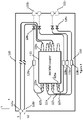
- Fig. 7 that shows a first embodiment of the current inventive concept, relates to a C-ROSA PIC where the OH function is delivered by a single MMI coupler component which is laid out in a "flip" configuration upon the C-ROSA PIC substrate.
- the MMI coupler "flip" configuration enables the interconnection of the MMI coupler output access waveguides to the PDs with non-intersecting integrated optical waveguides and without the intervention of any additional coupler elements.
- the integrated optical waveguides that connect the MMI coupler OH to the PDs can be flexibly laid out upon the waveguide routing area in a way to accommodate equal path lengths. As such the embodiment described below enables 75% coupler component reduction compared to the conventional C-ROSA PIC of Fig.
- the C-ROSA of the present disclosure minimizes design and fabrication complexity since the 4x4 MMI coupler is a standard, mature circuit and further to the MMI coupler, only passive integrated optical waveguides are deployed; as such no need for co-design and painstaking optimization of various interconnected coupler elements is required.
- Fig. 7 shows a C-ROSA PIC 100 comprising a substrate upon which the C-ROSA input/output ports and photonic components described below are disposed.
- substrate according to the present disclosure should be interpreted as material that is suitable for the photonic components to be fabricated thereon.
- C-ROSA PIC 100 comprises two optical input ports 101-A and 101-B and four electrical output ports 102-A through 102D - the position of the optical and electrical ports shown in Fig. 7 is exemplary and different locations maybe contemplated without deviating from the scope of the present invention.
- the input ports receive the S and LO optical signals whereas the output ports deliver electrical signals corresponding to the quadrature components of the demodulated input.
- the PIC further includes four PDs 106-A through 106-D forming two pairs of balanced PDs disposed upon the substrate in proximity to the C-ROSA electrical outputs 102-A through 102-D, with each PD connected to an electrical output via a conducting lead.
- the OH functionality is delivered by a single 4x4 MMI coupler having a main body 103, four attached input access waveguides 104-A through 104-D and four attached output access waveguides 105-A through 105-D.
- C-ROSA 100 uses the 4x4 MMI coupler with a layout suitable to avoid the requirement for a waveguide crossing.
- the 4x4 MMI coupler is arranged such that the plurality of input access waveguides 105-A through 105-D are facing the plurality of PDs 106-A through 106-D.
- Such configuration which may be called "flip" configuration, and with reference to the C-ROSA 60 described previously, may be realised by flipping the MMI coupler about a vertical axis.
- Two of the input access waveguides - in Fig. 7 104-A and 104-C - are configured to receive the S and LO signals from inputs 101-A and 101-B.
- the input access waveguides that receive S and LO signals are configured to launch light to the main body of the MMI coupler 103 and the plurality of output access waveguides 105A-D are configured to collect the multi-mode interference signal products from the MMI coupler main body 103.
- the OH functionality can be obtained, and the required 90-degree phase shifts are provided at the MMI coupler output access waveguides 105-A through 105-D.
- the S and LO mixing products are delivered at the MMI coupler output access waveguides as shown in Fig. 7 .
- the spacing between a pair of input access waveguides of the plurality of input access waveguides 104-A through 104-D and the spacing between a pair of output access waveguides of the plurality of output access waveguides 105-A through 105-D is uniform. In that way, effective operation with optimized coupling efficiency of the MMI coupler is ensured.
- each one of the plurality of the output access waveguides of the MMI coupler is connected to the plurality of PDs via integrated optical waveguides 107-A through 105-D. Due to the "flip" configuration of the MMI coupler, the intersection of the integrated optical waveguides 107-A through 107-D that connect the MMI coupler output access waveguides 105-A through 105-D to the PDs 106-A through 106-D is avoided.
- the optical waveguides interconnecting the MMI coupler output access waveguides 105-A through 105-D to PDs 106-A through 106-D are routed upon the waveguide routing area in a way that they exhibit equal lengths. This can be achieved by forming each one of the four optical paths with bent waveguide portions, straight waveguide portions or combination of both.
- the equal length of the waveguides is important in order to achieve phase matching of the signals arriving at the PDs.
- Fig. 8 that shows another embodiment, relates to a C-ROSA PIC that uses the same input ports, output ports, MMI coupler and PDs as the embodiment of Fig.7 and follows the same geometrical arrangement as the embodiment of Fig. 7 .
- C-ROSA PIC 120 comprises two optical input ports 121-A and 121-B and four electrical output ports 122-A through 122-D.
- the input ports receive the S and LO optical signals whereas the output ports deliver electrical signals corresponding to the quadrature components of the demodulated input.
- the PIC further includes four PDs 126-A through 106-D forming two pairs of balanced PDs disposed upon the substrate in proximity to the C-ROSA electrical outputs 102-A through 102-D, with each PD connected to an electrical output via a conducting lead.
- the OH functionality is delivered by a single 4x4 MMI coupler having a main body 123, four attached input access waveguides 124-A through 124-D and four attached output access waveguides 125-A through 125-D.
- C-ROSA 120 uses the 4x4 MMI coupler with the same "flip" configuration as the embodiment of fig. 7 to avoid waveguide crossings of the integrated optical waveguides interconnecting the plurality of the MMI coupler output access waveguides 125-A through 125-D to the plurality of PDs 122-A through 122-D.
- Two of the MMI coupler input access waveguides - in Fig. 8 124-A and 124-C - are configured to receive the S and LO signals from inputs 121-A and 121-B.
- the input access waveguides that receive S and LO signals are configured to launch light to the main body of the MMI coupler 123 and the plurality of output access waveguides 125-A through 125-D are configured to collect the multi-mode interference signal products from the MMI coupler main body 123.
- the OH functionality can be obtained, and the required 90-degree phase shifts are provided at the MMI coupler output access waveguides 125-A through 125-D.
- the S and LO mixing products are delivered at the MMI coupler output access waveguides as shown in Fig. 8 .
- the spacing between a pair of input access waveguides of the plurality of input access waveguides 124-A through 124-D and the spacing between a pair of output access waveguides of the plurality of output access waveguides 125-A through 125-D is uniform. In that way, effective operation with optimized coupling efficiency of the MMI coupler is ensured.
- each one of the plurality of the output access waveguides of the MMI coupler is connected to the plurality of PDs via integrated optical waveguides 127-A through 125-D. Due to the "flip" configuration of the MMI coupler, the intersection of the integrated optical waveguides 127-A through 127-D that connect the MMI coupler output access waveguides 125-A through 125-D to the PDs 126-A through 126-D is avoided.
- the integrated optical paths that connect the MMI coupler output ports 125-A through 125-D to PDs 126-A through 126-D are formed by a combination of passive integrated waveguide elements such as straight and bent waveguides assisted by active phase shifting elements 128-A through 128-D.
- phase shifting elements are advantageous since they enable phase fine tuning as well as precise matching of the lengths of the integrated optical waveguides.
- the rest of the components of the embodiment of fig. 8 are identical to those ones of the embodiment of fig. 7 .
- disclosed embodiments can also be applied to coherent communication systems where the S and LO optical signals will comprise a single polarization state, either a transverse magnetic (TM) or transverse electric (TE) type.
- TM transverse magnetic
- TE transverse electric
- disclosed embodiments can also be applied to coherent communication systems which deploy polarization multiplexing, where the S and LO optical signals will comprise both TM and TE polarizations.
- the optical coherent receiver will comprise two C-ROSA PICs of Fig. 7 or Fig. 8 disposed on a single or separate substrate and connected to polarization beam splitters.
- disclosed embodiments can also be applied to Wavelength Division multiplexing (WDM) coherent communication systems which deploy multiple S signals of different wavelength, where the optical coherent receiver will comprise an array of C-ROSA PICs of Fig. 7 or Fig. 8 disposed on a single or separate substrate - the number of C-ROSA PICs being the same as the number of the received signal wavelengths.
- WDM Wavelength Division multiplexing
Landscapes
- Physics & Mathematics (AREA)
- Electromagnetism (AREA)
- Engineering & Computer Science (AREA)
- Computer Networks & Wireless Communication (AREA)
- Signal Processing (AREA)
- Optical Integrated Circuits (AREA)
Priority Applications (4)
| Application Number | Priority Date | Filing Date | Title |
|---|---|---|---|
| EP21175458.5A EP4092932A1 (fr) | 2021-05-21 | 2021-05-21 | Un sous-ensemble optique de récepteur cohérent |
| US18/289,246 US12598003B2 (en) | 2021-05-21 | 2022-05-13 | Integrated coherent receiver having a single MMI coupler optical hybrid, non-intersecting optical paths and uniform electrical paths |
| EP22729484.0A EP4342106A1 (fr) | 2021-05-21 | 2022-05-13 | Récepteur cohérent intégré ayant un hybride optique à coupleur mmi unique, des trajets optiques non sécants et des trajets électriques uniformes |
| PCT/EP2022/063014 WO2022243184A1 (fr) | 2021-05-21 | 2022-05-13 | Récepteur cohérent intégré ayant un hybride optique à coupleur mmi unique, des trajets optiques non sécants et des trajets électriques uniformes |
Applications Claiming Priority (1)
| Application Number | Priority Date | Filing Date | Title |
|---|---|---|---|
| EP21175458.5A EP4092932A1 (fr) | 2021-05-21 | 2021-05-21 | Un sous-ensemble optique de récepteur cohérent |
Publications (1)
| Publication Number | Publication Date |
|---|---|
| EP4092932A1 true EP4092932A1 (fr) | 2022-11-23 |
Family
ID=76076237
Family Applications (2)
| Application Number | Title | Priority Date | Filing Date |
|---|---|---|---|
| EP21175458.5A Withdrawn EP4092932A1 (fr) | 2021-05-21 | 2021-05-21 | Un sous-ensemble optique de récepteur cohérent |
| EP22729484.0A Pending EP4342106A1 (fr) | 2021-05-21 | 2022-05-13 | Récepteur cohérent intégré ayant un hybride optique à coupleur mmi unique, des trajets optiques non sécants et des trajets électriques uniformes |
Family Applications After (1)
| Application Number | Title | Priority Date | Filing Date |
|---|---|---|---|
| EP22729484.0A Pending EP4342106A1 (fr) | 2021-05-21 | 2022-05-13 | Récepteur cohérent intégré ayant un hybride optique à coupleur mmi unique, des trajets optiques non sécants et des trajets électriques uniformes |
Country Status (3)
| Country | Link |
|---|---|
| US (1) | US12598003B2 (fr) |
| EP (2) | EP4092932A1 (fr) |
| WO (1) | WO2022243184A1 (fr) |
Families Citing this family (1)
| Publication number | Priority date | Publication date | Assignee | Title |
|---|---|---|---|---|
| CN118259514A (zh) * | 2024-03-28 | 2024-06-28 | 东南大学 | 一种相位补偿型硅基星形90度光混频器 |
Citations (3)
| Publication number | Priority date | Publication date | Assignee | Title |
|---|---|---|---|---|
| US20100166427A1 (en) * | 2008-12-26 | 2010-07-01 | Fujitsu Limited | Optical hybrid circuit, optical receiver and light receiving method |
| US20160285561A1 (en) * | 2015-03-23 | 2016-09-29 | ArtlC Photonics Inc. | Integrated Coherent Receiver Having a Geometric Arrangement for Improved Device Efficiency |
| US10126498B1 (en) * | 2017-07-25 | 2018-11-13 | Elenion Technologies, Llc | Optical hybrid |
Family Cites Families (8)
| Publication number | Priority date | Publication date | Assignee | Title |
|---|---|---|---|---|
| EP2624513B1 (fr) * | 2009-02-17 | 2014-06-25 | Oclaro Technology Limited | Puces optiques et dispositifs pour communications optiques |
| JP5640829B2 (ja) * | 2011-03-09 | 2014-12-17 | 富士通株式会社 | 光ハイブリッド回路、光受信機及び光受信方法 |
| US20170207603A1 (en) * | 2015-04-29 | 2017-07-20 | Infinera Corporation | Laser arrays comprising compact lasers with extended tunability |
| US10805011B2 (en) * | 2016-03-29 | 2020-10-13 | Nokia Technologies Oy | Bell state measurement |
| US11171466B2 (en) * | 2018-01-18 | 2021-11-09 | Lumentum Operations Llc | On-chip wavelength locker |
| CN112567651B (zh) * | 2018-08-10 | 2024-03-12 | 诺基亚技术有限公司 | 基于光纤的通信 |
| JP7467985B2 (ja) * | 2020-02-28 | 2024-04-16 | 富士通オプティカルコンポーネンツ株式会社 | 光デバイスおよび光デバイスの試験方法 |
| US11333831B2 (en) * | 2020-09-21 | 2022-05-17 | Ii-Vi Delaware, Inc. | Optical couplers and hybrids |
-
2021
- 2021-05-21 EP EP21175458.5A patent/EP4092932A1/fr not_active Withdrawn
-
2022
- 2022-05-13 WO PCT/EP2022/063014 patent/WO2022243184A1/fr not_active Ceased
- 2022-05-13 US US18/289,246 patent/US12598003B2/en active Active
- 2022-05-13 EP EP22729484.0A patent/EP4342106A1/fr active Pending
Patent Citations (5)
| Publication number | Priority date | Publication date | Assignee | Title |
|---|---|---|---|---|
| US20100166427A1 (en) * | 2008-12-26 | 2010-07-01 | Fujitsu Limited | Optical hybrid circuit, optical receiver and light receiving method |
| US8280256B2 (en) | 2008-12-26 | 2012-10-02 | Fujitsu Limited | Optical hybrid circuit, optical receiver and light receiving method |
| US20160285561A1 (en) * | 2015-03-23 | 2016-09-29 | ArtlC Photonics Inc. | Integrated Coherent Receiver Having a Geometric Arrangement for Improved Device Efficiency |
| US10126498B1 (en) * | 2017-07-25 | 2018-11-13 | Elenion Technologies, Llc | Optical hybrid |
| US20200096699A1 (en) | 2017-07-25 | 2020-03-26 | Elenion Technologies, Llc | Optical hybrid |
Non-Patent Citations (1)
| Title |
|---|
| FARALLI S ET AL: "A Compact Silicon Coherent Receiver Without Waveguide Crossing", IEEE PHOTONICS JOURNAL, IEEE, USA, vol. 7, no. 4, 1 August 2015 (2015-08-01), pages 1 - 6, XP011664992, DOI: 10.1109/JPHOT.2015.2456632 * |
Also Published As
| Publication number | Publication date |
|---|---|
| US20240259108A1 (en) | 2024-08-01 |
| EP4342106A1 (fr) | 2024-03-27 |
| WO2022243184A1 (fr) | 2022-11-24 |
| US12598003B2 (en) | 2026-04-07 |
Similar Documents
| Publication | Publication Date | Title |
|---|---|---|
| US10901148B2 (en) | Optical hybrid | |
| CN107925484B (zh) | 一种单片集成相干光接收器芯片 | |
| US11579361B2 (en) | TeraPHY chiplet optical input/output system | |
| CN102396196B (zh) | 用于光学通信的光学芯片和器件 | |
| US11740411B2 (en) | Optical couplers and hybrids | |
| US11982839B2 (en) | Optical 90 degree hybrid circuit | |
| JP2021190645A (ja) | 光集積素子、及び光集積回路 | |
| US8478090B2 (en) | Optical waveguide device and manufacturing method of optical waveguide device | |
| EP4092932A1 (fr) | Un sous-ensemble optique de récepteur cohérent | |
| CN114114529A (zh) | 用于高信道计数光子学的光学再分布层 | |
| CN114365033A (zh) | Iq光调制器 | |
| Gunn et al. | A 40Gbps CMOS photonics transceiver | |
| WO2019222476A1 (fr) | Agencement d'entrée/sortie optique pour circuits photoniques intégrés | |
| JPH1130722A (ja) | 光モジュール | |
| US20240248260A1 (en) | Optical flow switching using photonic integrated circuits | |
| EP4716115A1 (fr) | Dispositif de mise en réseau optique | |
| WO1991013376A1 (fr) | Duplexeur optique | |
| Gunn et al. | A 40Gb CMOS photonics transceiver |
Legal Events
| Date | Code | Title | Description |
|---|---|---|---|
| PUAI | Public reference made under article 153(3) epc to a published international application that has entered the european phase |
Free format text: ORIGINAL CODE: 0009012 |
|
| STAA | Information on the status of an ep patent application or granted ep patent |
Free format text: STATUS: THE APPLICATION HAS BEEN PUBLISHED |
|
| AK | Designated contracting states |
Kind code of ref document: A1 Designated state(s): AL AT BE BG CH CY CZ DE DK EE ES FI FR GB GR HR HU IE IS IT LI LT LU LV MC MK MT NL NO PL PT RO RS SE SI SK SM TR |
|
| STAA | Information on the status of an ep patent application or granted ep patent |
Free format text: STATUS: REQUEST FOR EXAMINATION WAS MADE |
|
| 17P | Request for examination filed |
Effective date: 20230519 |
|
| RBV | Designated contracting states (corrected) |
Designated state(s): AL AT BE BG CH CY CZ DE DK EE ES FI FR GB GR HR HU IE IS IT LI LT LU LV MC MK MT NL NO PL PT RO RS SE SI SK SM TR |
|
| STAA | Information on the status of an ep patent application or granted ep patent |
Free format text: STATUS: THE APPLICATION IS DEEMED TO BE WITHDRAWN |
|
| 18D | Application deemed to be withdrawn |
Effective date: 20241203 |