EP4093162A1 - Komponententräger mit einem magnetischen element und herstellungsverfahren - Google Patents
Komponententräger mit einem magnetischen element und herstellungsverfahren Download PDFInfo
- Publication number
- EP4093162A1 EP4093162A1 EP21174488.3A EP21174488A EP4093162A1 EP 4093162 A1 EP4093162 A1 EP 4093162A1 EP 21174488 A EP21174488 A EP 21174488A EP 4093162 A1 EP4093162 A1 EP 4093162A1
- Authority
- EP
- European Patent Office
- Prior art keywords
- layer structure
- magnetic
- magnetic element
- dielectric layer
- component carrier
- Prior art date
- Legal status (The legal status is an assumption and is not a legal conclusion. Google has not performed a legal analysis and makes no representation as to the accuracy of the status listed.)
- Pending
Links
Images


Classifications
-
- H—ELECTRICITY
- H05—ELECTRIC TECHNIQUES NOT OTHERWISE PROVIDED FOR
- H05K—PRINTED CIRCUITS; CASINGS OR CONSTRUCTIONAL DETAILS OF ELECTRIC APPARATUS; MANUFACTURE OF ASSEMBLAGES OF ELECTRICAL COMPONENTS
- H05K1/00—Printed circuits
- H05K1/16—Printed circuits incorporating printed electric components, e.g. printed resistors, capacitors or inductors
- H05K1/165—Printed circuits incorporating printed electric components, e.g. printed resistors, capacitors or inductors incorporating printed inductors
-
- H—ELECTRICITY
- H01—ELECTRIC ELEMENTS
- H01F—MAGNETS; INDUCTANCES; TRANSFORMERS; SELECTION OF MATERIALS FOR THEIR MAGNETIC PROPERTIES
- H01F17/00—Fixed inductances of the signal type
- H01F17/0006—Printed inductances
- H01F17/0013—Printed inductances with stacked layers
-
- H—ELECTRICITY
- H01—ELECTRIC ELEMENTS
- H01F—MAGNETS; INDUCTANCES; TRANSFORMERS; SELECTION OF MATERIALS FOR THEIR MAGNETIC PROPERTIES
- H01F17/00—Fixed inductances of the signal type
- H01F17/0006—Printed inductances
-
- H—ELECTRICITY
- H01—ELECTRIC ELEMENTS
- H01F—MAGNETS; INDUCTANCES; TRANSFORMERS; SELECTION OF MATERIALS FOR THEIR MAGNETIC PROPERTIES
- H01F27/00—Details of transformers or inductances, in general
- H01F27/28—Coils; Windings; Conductive connections
- H01F27/2804—Printed windings
-
- H—ELECTRICITY
- H01—ELECTRIC ELEMENTS
- H01F—MAGNETS; INDUCTANCES; TRANSFORMERS; SELECTION OF MATERIALS FOR THEIR MAGNETIC PROPERTIES
- H01F41/00—Apparatus or processes specially adapted for manufacturing or assembling magnets, inductances or transformers; Apparatus or processes specially adapted for manufacturing materials characterised by their magnetic properties
-
- H—ELECTRICITY
- H01—ELECTRIC ELEMENTS
- H01F—MAGNETS; INDUCTANCES; TRANSFORMERS; SELECTION OF MATERIALS FOR THEIR MAGNETIC PROPERTIES
- H01F41/00—Apparatus or processes specially adapted for manufacturing or assembling magnets, inductances or transformers; Apparatus or processes specially adapted for manufacturing materials characterised by their magnetic properties
- H01F41/02—Apparatus or processes specially adapted for manufacturing or assembling magnets, inductances or transformers; Apparatus or processes specially adapted for manufacturing materials characterised by their magnetic properties for manufacturing cores, coils, or magnets
- H01F41/04—Apparatus or processes specially adapted for manufacturing or assembling magnets, inductances or transformers; Apparatus or processes specially adapted for manufacturing materials characterised by their magnetic properties for manufacturing cores, coils, or magnets for manufacturing coils
- H01F41/041—Printed circuit coils
- H01F41/046—Printed circuit coils structurally combined with ferromagnetic material
-
- H—ELECTRICITY
- H05—ELECTRIC TECHNIQUES NOT OTHERWISE PROVIDED FOR
- H05K—PRINTED CIRCUITS; CASINGS OR CONSTRUCTIONAL DETAILS OF ELECTRIC APPARATUS; MANUFACTURE OF ASSEMBLAGES OF ELECTRICAL COMPONENTS
- H05K1/00—Printed circuits
- H05K1/02—Details
-
- H—ELECTRICITY
- H05—ELECTRIC TECHNIQUES NOT OTHERWISE PROVIDED FOR
- H05K—PRINTED CIRCUITS; CASINGS OR CONSTRUCTIONAL DETAILS OF ELECTRIC APPARATUS; MANUFACTURE OF ASSEMBLAGES OF ELECTRICAL COMPONENTS
- H05K1/00—Printed circuits
- H05K1/02—Details
- H05K1/09—Use of materials for the conductive, e.g. metallic pattern
-
- H—ELECTRICITY
- H05—ELECTRIC TECHNIQUES NOT OTHERWISE PROVIDED FOR
- H05K—PRINTED CIRCUITS; CASINGS OR CONSTRUCTIONAL DETAILS OF ELECTRIC APPARATUS; MANUFACTURE OF ASSEMBLAGES OF ELECTRICAL COMPONENTS
- H05K1/00—Printed circuits
- H05K1/18—Printed circuits structurally associated with non-printed electric components
- H05K1/182—Printed circuits structurally associated with non-printed electric components associated with components mounted in printed circuit boards [PCB], e.g. insert-mounted components [IMC]
- H05K1/183—Printed circuits structurally associated with non-printed electric components associated with components mounted in printed circuit boards [PCB], e.g. insert-mounted components [IMC] associated with components mounted in and supported by recessed areas of the PCBs
-
- H—ELECTRICITY
- H05—ELECTRIC TECHNIQUES NOT OTHERWISE PROVIDED FOR
- H05K—PRINTED CIRCUITS; CASINGS OR CONSTRUCTIONAL DETAILS OF ELECTRIC APPARATUS; MANUFACTURE OF ASSEMBLAGES OF ELECTRICAL COMPONENTS
- H05K3/00—Apparatus or processes for manufacturing printed circuits
- H05K3/02—Apparatus or processes for manufacturing printed circuits in which the conductive material is applied to the surface of the insulating support and is thereafter removed from such areas of the surface which are not intended for current conducting or shielding
- H05K3/06—Apparatus or processes for manufacturing printed circuits in which the conductive material is applied to the surface of the insulating support and is thereafter removed from such areas of the surface which are not intended for current conducting or shielding the conductive material being removed chemically or electrolytically, e.g. by photo-etch process
-
- H—ELECTRICITY
- H05—ELECTRIC TECHNIQUES NOT OTHERWISE PROVIDED FOR
- H05K—PRINTED CIRCUITS; CASINGS OR CONSTRUCTIONAL DETAILS OF ELECTRIC APPARATUS; MANUFACTURE OF ASSEMBLAGES OF ELECTRICAL COMPONENTS
- H05K3/00—Apparatus or processes for manufacturing printed circuits
- H05K3/10—Apparatus or processes for manufacturing printed circuits in which conductive material is applied to the insulating support in such a manner as to form the desired conductive pattern
- H05K3/12—Apparatus or processes for manufacturing printed circuits in which conductive material is applied to the insulating support in such a manner as to form the desired conductive pattern using thick film techniques, e.g. printing techniques to apply the conductive material or similar techniques for applying conductive paste or ink patterns
- H05K3/1216—Apparatus or processes for manufacturing printed circuits in which conductive material is applied to the insulating support in such a manner as to form the desired conductive pattern using thick film techniques, e.g. printing techniques to apply the conductive material or similar techniques for applying conductive paste or ink patterns by screen printing or stencil printing
-
- H—ELECTRICITY
- H05—ELECTRIC TECHNIQUES NOT OTHERWISE PROVIDED FOR
- H05K—PRINTED CIRCUITS; CASINGS OR CONSTRUCTIONAL DETAILS OF ELECTRIC APPARATUS; MANUFACTURE OF ASSEMBLAGES OF ELECTRICAL COMPONENTS
- H05K3/00—Apparatus or processes for manufacturing printed circuits
- H05K3/46—Manufacturing multilayer circuits
- H05K3/4611—Manufacturing multilayer circuits by laminating two or more circuit boards
-
- H—ELECTRICITY
- H05—ELECTRIC TECHNIQUES NOT OTHERWISE PROVIDED FOR
- H05K—PRINTED CIRCUITS; CASINGS OR CONSTRUCTIONAL DETAILS OF ELECTRIC APPARATUS; MANUFACTURE OF ASSEMBLAGES OF ELECTRICAL COMPONENTS
- H05K3/00—Apparatus or processes for manufacturing printed circuits
- H05K3/46—Manufacturing multilayer circuits
- H05K3/4644—Manufacturing multilayer circuits by building the multilayer layer by layer, i.e. build-up multilayer circuits
- H05K3/465—Manufacturing multilayer circuits by building the multilayer layer by layer, i.e. build-up multilayer circuits by applying an insulating layer having channels for the next circuit layer
-
- H—ELECTRICITY
- H01—ELECTRIC ELEMENTS
- H01F—MAGNETS; INDUCTANCES; TRANSFORMERS; SELECTION OF MATERIALS FOR THEIR MAGNETIC PROPERTIES
- H01F17/00—Fixed inductances of the signal type
- H01F17/0006—Printed inductances
- H01F2017/0073—Printed inductances with a special conductive pattern, e.g. flat spiral
-
- H—ELECTRICITY
- H01—ELECTRIC ELEMENTS
- H01F—MAGNETS; INDUCTANCES; TRANSFORMERS; SELECTION OF MATERIALS FOR THEIR MAGNETIC PROPERTIES
- H01F17/00—Fixed inductances of the signal type
- H01F17/04—Fixed inductances of the signal type with magnetic core
- H01F2017/048—Fixed inductances of the signal type with magnetic core with encapsulating core, e.g. made of resin and magnetic powder
-
- H—ELECTRICITY
- H01—ELECTRIC ELEMENTS
- H01F—MAGNETS; INDUCTANCES; TRANSFORMERS; SELECTION OF MATERIALS FOR THEIR MAGNETIC PROPERTIES
- H01F41/00—Apparatus or processes specially adapted for manufacturing or assembling magnets, inductances or transformers; Apparatus or processes specially adapted for manufacturing materials characterised by their magnetic properties
- H01F41/02—Apparatus or processes specially adapted for manufacturing or assembling magnets, inductances or transformers; Apparatus or processes specially adapted for manufacturing materials characterised by their magnetic properties for manufacturing cores, coils, or magnets
- H01F41/04—Apparatus or processes specially adapted for manufacturing or assembling magnets, inductances or transformers; Apparatus or processes specially adapted for manufacturing materials characterised by their magnetic properties for manufacturing cores, coils, or magnets for manufacturing coils
- H01F41/041—Printed circuit coils
- H01F41/042—Printed circuit coils by thin film techniques
-
- H—ELECTRICITY
- H05—ELECTRIC TECHNIQUES NOT OTHERWISE PROVIDED FOR
- H05K—PRINTED CIRCUITS; CASINGS OR CONSTRUCTIONAL DETAILS OF ELECTRIC APPARATUS; MANUFACTURE OF ASSEMBLAGES OF ELECTRICAL COMPONENTS
- H05K2201/00—Indexing scheme relating to printed circuits covered by H05K1/00
- H05K2201/03—Conductive materials
- H05K2201/0332—Structure of the conductor
- H05K2201/0335—Layered conductors or foils
- H05K2201/0358—Resin coated copper [RCC]
-
- H—ELECTRICITY
- H05—ELECTRIC TECHNIQUES NOT OTHERWISE PROVIDED FOR
- H05K—PRINTED CIRCUITS; CASINGS OR CONSTRUCTIONAL DETAILS OF ELECTRIC APPARATUS; MANUFACTURE OF ASSEMBLAGES OF ELECTRICAL COMPONENTS
- H05K2201/00—Indexing scheme relating to printed circuits covered by H05K1/00
- H05K2201/03—Conductive materials
- H05K2201/0332—Structure of the conductor
- H05K2201/0364—Conductor shape
- H05K2201/0376—Flush conductors, i.e. flush with the surface of the printed circuit
-
- H—ELECTRICITY
- H05—ELECTRIC TECHNIQUES NOT OTHERWISE PROVIDED FOR
- H05K—PRINTED CIRCUITS; CASINGS OR CONSTRUCTIONAL DETAILS OF ELECTRIC APPARATUS; MANUFACTURE OF ASSEMBLAGES OF ELECTRICAL COMPONENTS
- H05K2201/00—Indexing scheme relating to printed circuits covered by H05K1/00
- H05K2201/08—Magnetic details
-
- H—ELECTRICITY
- H05—ELECTRIC TECHNIQUES NOT OTHERWISE PROVIDED FOR
- H05K—PRINTED CIRCUITS; CASINGS OR CONSTRUCTIONAL DETAILS OF ELECTRIC APPARATUS; MANUFACTURE OF ASSEMBLAGES OF ELECTRICAL COMPONENTS
- H05K2203/00—Indexing scheme relating to apparatus or processes for manufacturing printed circuits covered by H05K3/00
- H05K2203/07—Treatments involving liquids, e.g. plating, rinsing
- H05K2203/0703—Plating
- H05K2203/072—Electroless plating, e.g. finish plating or initial plating
-
- H—ELECTRICITY
- H05—ELECTRIC TECHNIQUES NOT OTHERWISE PROVIDED FOR
- H05K—PRINTED CIRCUITS; CASINGS OR CONSTRUCTIONAL DETAILS OF ELECTRIC APPARATUS; MANUFACTURE OF ASSEMBLAGES OF ELECTRICAL COMPONENTS
- H05K2203/00—Indexing scheme relating to apparatus or processes for manufacturing printed circuits covered by H05K3/00
- H05K2203/30—Details of processes not otherwise provided for in H05K2203/01 - H05K2203/17
- H05K2203/308—Sacrificial means, e.g. for temporarily filling a space for making a via or a cavity or for making rigid-flexible PCBs
-
- H—ELECTRICITY
- H05—ELECTRIC TECHNIQUES NOT OTHERWISE PROVIDED FOR
- H05K—PRINTED CIRCUITS; CASINGS OR CONSTRUCTIONAL DETAILS OF ELECTRIC APPARATUS; MANUFACTURE OF ASSEMBLAGES OF ELECTRICAL COMPONENTS
- H05K3/00—Apparatus or processes for manufacturing printed circuits
- H05K3/10—Apparatus or processes for manufacturing printed circuits in which conductive material is applied to the insulating support in such a manner as to form the desired conductive pattern
- H05K3/12—Apparatus or processes for manufacturing printed circuits in which conductive material is applied to the insulating support in such a manner as to form the desired conductive pattern using thick film techniques, e.g. printing techniques to apply the conductive material or similar techniques for applying conductive paste or ink patterns
- H05K3/1258—Apparatus or processes for manufacturing printed circuits in which conductive material is applied to the insulating support in such a manner as to form the desired conductive pattern using thick film techniques, e.g. printing techniques to apply the conductive material or similar techniques for applying conductive paste or ink patterns by using a substrate provided with a shape pattern, e.g. grooves, banks, resist pattern
Definitions
- the invention relates to a component carrier with a magnetic element and a dielectric layer structure.
- the invention further relates to a method of manufacturing the component carrier. Further, the invention related to a method of using photo-imaging in a specific manner. Accordingly, the invention may relate to the technical field of magnetic/inductive applications in component carriers such as printed circuit boards or IC substrates.
- component carriers equipped with one or more electronic components and increasing miniaturization of such electronic components as well as a rising number of electronic components to be mounted on the component carriers such as printed circuit boards
- increasingly more powerful array-like components or packages having several electronic components are being employed, which have a plurality of contacts or connections, with ever smaller spacing between these contacts.
- Removal of heat generated by such electronic components and the component carrier itself during operation becomes an increasing issue.
- an efficient protection against electromagnetic interference (EMI) becomes an increasing issue.
- component carriers shall be mechanically robust and electrically and magnetically reliable so as to be operable even under harsh conditions.
- Figure 2 shows a conventional example, wherein a magnetic element is surface-mounted to a circuit board 400.
- a component carrier, a method of manufacturing, and a use according to the independent claims are provided.
- a component carrier comprising:
- a method of manufacturing a component carrier comprising:
- an inductive element e.g. a coil
- a component carrier in an (essentially) drill-free manner
- magnetic element may refer to any element suitable to be incorporated into a component carrier (such as a circuit board) and which element comprises magnetic properties.
- the magnetic element may comprise any shape according to the desired functionality, e.g. rectangular (in particular in form of a block), circular, polygonal, etc.
- a magnetic element may comprise a magnetic matrix (see definition below) into which an inductive element may be placed/embedded.
- a magnetic element may comprise a magnetic paste.
- the magnetic element is arranged in the component carrier in a planar manner (with the directions of main extension being parallel to the component carrier directions of main extension, in other words: arranged horizontally).
- the magnetic element may be essentially shaped as a plate and/or planar, meaning that it comprises two directions of main extension along the x- and y-axes (with respect to the component carrier) and a comparably short extension along the z-axis.
- the term “horizontal” may thus mean “oriented in parallel with a direction of main extension”
- the term “vertical” may mean “oriented perpendicular to the directions of main extension”.
- magnetic matrix may in particular refer to a base material (base substance) that comprises magnetic properties.
- the base material may be magnetic itself or magnetic particles may be distributed within a non-magnetic matrix material.
- the magnetic matrix may be configured for example rigid/solid (e.g. as magnetic sheets) or viscous (magnetic paste).
- the magnetic matrix may comprise electrically conductive material/particles and/or electrically insulating material/particles. Further, the magnetic matrix may be configured to have a relative magnetic permeability ⁇ r in a range from 2 to 10 6 .
- a plurality of different materials may be considered suitable to provide the base material and/or the embedded particles of the magnetic matrix, for example a ferromagnetic material (like iron), a ferrimagnetic material (like ferrite), a permanent magnetic material, a soft magnetic material, a metal oxide.
- a dielectric (resin) matrix with magnetic particles therein is used.
- magnetic sheets are applied that comprise magnetic particles embedded in a fiber-enforced resin (e.g. prepreg).
- a magnetic paste is used that comprises magnetic particles embedded in a not fiber-enforced resin.
- dielectric layer structure may refer to any dielectric material that can be formed (in particular laminated) as a component carrier layer structure. Further, a cavity may be formed in the dielectric layer structure, in particular by using one of photo-imaging, etching, pre-cutting.
- the term "photo-imageable dielectric layer structure” may refer to any dielectric (layer) structure that is configured to be treated (shows an effect) using photo-imaging.
- the term refers to a PID dielectric layer structure into which a cavity can be formed using (only) photo-imaging techniques.
- a PID layer structure comprises a non-fiber enforced resin, e.g. polyimide.
- a base material for a PID application may include: i) thermosetting material, e.g. epoxy, BCB, phenol, ii) thermoplastic material: PI, PBO.
- the PID material may further comprise a photo initiator (photo sensitive agent) that may be cured by photo UV light.
- the PID material may be laminated on a substrate (e.g. the stack) and may then be exposed to a lithographic source via a pattern mask, wherein the pattern mask defines the to be manufactured cavities. A portion of the PID material may be developed and one of an exposed portion and an unexposed portion (positive or negative photolithography may be used) may be removed to obtain a plurality of cavities. Examples of photolithography processes may include X-ray lithography, UV lithography, stereo lithography, e-beam lithography and laser lithography.
- component carrier may particularly denote any support structure which is capable of accommodating one or more components thereon and/or therein for providing mechanical support and/or electrical connectivity.
- a component carrier may be configured as a mechanical and/or electronic carrier for components.
- a component carrier may be one of a printed circuit board, an organic interposer, a metal core substrate, an inorganic substrate and an IC (integrated circuit) substrate.
- a component carrier may also be a hybrid board combining different ones of the above mentioned types of component carriers.
- the invention may be based on the idea that a high magnetically enhanced inductance (value) for a component carrier can be provided in a cost-efficient manner, when a magnetic element with an embedded inductive element is assembled to the component carrier, wherein the magnetic element is surrounded by a dielectric (for example PID) layer structure of the component carrier.
- a dielectric for example PID
- This specific design directly reflects a manufacturing method of providing a cavity in the dielectric layer structure, using e.g. one of photo-lithography, etching, or (core) pre-cutting, and placing the magnetic element into the cavity, so that the magnetic element is surrounded (embedded) by the dielectric material.
- the manufacturing process may be performed in two steps of dielectric layer structure lamination, wherein only a first (lower) part of the magnetic element is placed in a first cavity of a first dielectric layer structure, before a second cavity is formed in a second dielectric layer structure (above the first dielectric layer structure) to enable arranging a second (upper) part of the magnetic element on top of the first magnetic element.
- a two-step approach may enable embedding the inductive element (e.g. in form of a copper coil) in between the first magnetic element and the second magnetic element directly within the component carrier manufacturing process.
- the inventors have now found that it may be surprisingly efficient to provide the magnetic material as a (planar oriented) magnetic element into a cavity formed in a dielectric layer structure of the component carrier.
- a higher inductance value can be provided, since a larger amount of magnetic material (and accordingly more and larger magnetic particles) may be embedded in component carrier material.
- the (e.g. photo-lithography) process for forming the cavities in dielectric material may be easily and cost-efficiently realized also at a large scale.
- the significantly improved inductance values may be in particular suitable for specific applications such as clients (processors), smartphones, wearables, and medical applications.
- the magnetic element comprises a magnetic matrix, and an electrically conductive structure (e.g. a copper trace) that is (at least partially) (in particular fully) embedded in the magnetic matrix to provide the inductive element.
- an electrically conductive structure e.g. a copper trace
- a planar inductive element may be provided in an efficient, robust, and cost-saving manner.
- the magnetic matrix may encapsulate (fully) the electrically conductive structure and thus significantly increase the inductance value.
- a magnetic element planar
- a large amount of magnetic material may be applied (in comparison to coaxial inductors) which may lead to a higher inductance value.
- the electrically conductive structure is formed as a winding (in particular a coil-like structure). This may provide the advantage that an inductance may be easily provided merely by the form of the electrically conductive structure.
- winding may particularly denote a loop structure (which may be similar to a helical structure with corners), wherein multiple of such loops may form a coil-type arrangement.
- the windings of the coil (like) structure may have edge-like or corner-like portions rather than being limited to a composition of multiple interconnected purely circular structures.
- the directions of main extension (length x and width) of the winding are (essentially) parallel to the directions of main extension (length x and width y) of the component carrier.
- the magnetic element and the component carrier are plate-shaped (in particular planar), they may be oriented in parallel with respect to each other. This may provide the advantage of a high inductance value (see above) that can be provided in an easy manner.
- the magnetic field of a horizontally (planar) oriented magnetic element may be perpendicular when compared with a magnetic field of a conventional coaxial winding (with respect to the component carrier).
- the dielectric layer structure comprises a shift pattern that reflects a manufacturing step of laminating a second dielectric layer structure on a first dielectric layer structure to form the dielectric layer structure (see also Figures 6h-k below).
- This may provide the specific advantage that the inductive element may be efficiently enclosed in the magnetic matrix directly during the component carrier manufacturing (during layer build-up).
- at least two dielectric layer structures (and two corresponding cavities) may be applied to embed the inductive element within the magnetic element.
- the shift pattern may be observable visually or using a microscope.
- the shift pattern comprises at least one of the group which consists of an alignment shift, a smearing, a tapering of a dielectric layer structure sidewall being in contact with a sidewall of the magnetic element.
- the shift pattern is established along a plane being (essentially) flush to an upper main surface of the electrically conductive structure and being (essentially) parallel to the directions of main extension (x, y) of the component carrier.
- a further shift pattern may be present at an interface between the first magnetic element and the second magnetic element, in particular along a plane being (essentially) flush to an upper main surface of the electrically conductive structure and being (essentially) parallel to the directions of main extension (x, y) of the component carrier.
- a lower main surface of the magnetic element is flush with an upper main surface of the layer stack. In this manner, the magnetic element can be directly applied on component carrier material.
- an upper main surface of the magnetic element is flush with an upper main surface of the dielectric layer structure.
- the magnetic element may perfectly fit in the (at least two) cavities and a further layer structure may be directly build-up on the component carrier.
- the component carrier further comprises a further layer structure and/or a further stack arranged on the dielectric layer structure and/or on the magnetic element.
- a further build-up can be done in an efficient and robust manner.
- the magnetic element may be sandwiched between several component carrier layers or between two or more layer stacks.
- the magnetic matrix continuously fills a volume around the electrically conductive structure and between windings of the electrically conductive structure (see e.g. Figure 3 ).
- This may provide the advantage that the electrically conductive structure is enclosed in a stable and robust manner. Further, this may provide the advantage that a high amount of magnetic material can be applied, and an accordingly high inductance can be achieved.
- the described (planar) magnetic element may allow for applying a high amount of magnetic matrix (that fills all the space between the vias).
- the magnetic matrix comprises at least one of the group consisting of a rigid solid, and a paste.
- the magnetic matrix may be configured as a magnetic sheet (rigid) that can be laminated.
- the magnetic matrix may comprise a prepreg or another resin with embedded magnetic particles.
- the magnetic matrix may be configured as a magnetic paste (viscous) that could be filled/poured in a mold to manufacture the magnetic element.
- the magnetic matrix comprises one of the group which consists of: electrically conductive, electrically insulating, partially electrically conductive and partially electrically insulating (e.g. a first electrically conductive part and a second electrically insulating part).
- electrically conductive, electrically insulating, partially electrically conductive and partially electrically insulating e.g. a first electrically conductive part and a second electrically insulating part.
- different configurations of the magnetic matrix may be especially suitable.
- the relative magnetic permeability ⁇ r of the magnetic matrix is in a range from 2 to 10 6 , in particular 2 to 1000, more in particular 20 to 80, more in particular around 50. These values are comparably high and can lead to an advantageously high inductance value. Permeability is the measure of magnetization that a material obtains in response to an applied magnetic field.
- the relative permeability denoted by the symbol ⁇ r , is the ratio of the permeability of a specific medium ⁇ to the permeability of free space ⁇ 0 (vacuum).
- the magnetic matrix comprises at least one material of the group consisting of a ferromagnetic material (e.g. iron, nickel), a ferrimagnetic material, a permanent magnetic material, a soft magnetic material, a ferrite, a metal oxide (e.g. magnetite), a dielectric matrix (e.g. a resin), in particular a prepreg, with magnetic particles therein, and an alloy, in particular an iron alloy or alloyed silicon.
- a ferromagnetic material e.g. iron, nickel
- ferrimagnetic material e.g. iron, nickel
- a ferrimagnetic material e.g. iron, nickel
- a ferrimagnetic material e.g. iron, nickel
- a ferrimagnetic material e.g. iron, nickel
- a ferrimagnetic material e.g. iron, nickel
- a ferrimagnetic material e.g. iron, nickel
- a ferrimagnetic material e.g. iron, nickel
- a permanent magnetic material may be ferromagnetic material or ferrimagnetic material, and may for instance be provided on the basis of transition metals (with partially filled 3d shell) such as iron or nickel, or on the basis of rare earths (with partially filled 4f shell).
- a soft magnetic material may be a material which can be easily re-magnetized, i.e. having a small area of its hysteresis curve.
- soft magnetic materials are those materials that are easily magnetized and demagnetized. They may have intrinsic coercivity less than 1000 Am -1 .
- a ferrite may be denoted as a type of ceramic compound composed of Fe 2 O 3 combined chemically with one or more additional metallic elements.
- Ferrites are both electrically non-conductive and ferrimagnetic, so they can be magnetized or attracted by a magnet.
- Ferrites may be implemented as hard ferrites or soft ferrites, depending on the application.
- placing (e.g. by screen printing) the first magnetic element further comprises: providing a plurality of gaps within the first magnetic element, and arranging an electrically conductive structure at least partially in the gaps (in particular in form of windings), so that an inductive element is provided.
- embedding the inductive element is directly integrated within the component carrier manufacturing process.
- Providing the gaps may e.g. include etching, mechanical drilling, or laser drilling.
- the gaps may be arranged in form of a winding to provide a mold for the electrically conductive structure.
- Said electrically conductive structure may be arranged by electroplating (e.g. copper) within the gaps, preferably in form of the windings.
- arranging the electrically conductive structure further comprises providing a seed-layer (e.g. electro-less plating and/or sputtering) to cover a respective bottom of the plurality of gaps. Then, the filling the gaps may be (at least partially) (in particular fully) by electro-plating.
- a seed-layer e.g. electro-less plating and/or sputtering
- placing the second magnetic element further comprises: arranging the second magnetic element on (in particular directly on) the first magnetic element in order to embed the electrically conductive structure within magnetic material.
- the first magnetic element comprises a first magnetic matrix
- the second magnetic element comprises a second magnetic matrix
- the first magnetic matrix and the second magnetic matrix comprise a similar material or a different material.
- forming the second cavity further comprises: exposing an upper main surface of the first magnetic element.
- the upper main surface of the first magnetic element is directly operable and, for example, the second magnetic element can be connected directly.
- arranging the first dielectric layer structure and/or the second dielectric layer structure comprises lamination using at least one of heat and pressure. This may provide the advantage that an established industry-relevant component carrier manufacturing technique can be directly applied.
- the dielectric layer structure is a PID layer structure
- forming the first cavity and/or the second cavity comprises: exposing a part of the first PID layer structure and/or the second PID layer structure to photo-imaging, in particular photolithography.
- forming the first cavity and/or the second cavity comprises removing a part of the first dielectric layer structure and/or the second dielectric layer structure by etching or (core) pre-cutting (e.g. mechanical or laser).
- the dielectric layer structure comprises a cavity
- the magnetic element is at least partially (in particular fully) embedded in the cavity.
- placing the first magnetic element and/or the second magnetic element further comprises screen printing. This may provide the advantage that an established industry-relevant component carrier manufacturing technique can be directly applied.
- the magnetic element may be configured for shielding electromagnetic radiation from propagating within the component carrier or within the stack (for instance from a first portion of the stack to a second portion of the stack).
- the magnetic element may however also be configured for shielding electromagnetic radiation from propagating between component carrier and an environment.
- Such a shielding may include a prevention of electromagnetic radiation from propagating from an exterior of the component carrier to an interior of the component carrier, from an interior of the component carrier to an exterior of the component carrier, and/or between different portions of the component carrier.
- such a shielding may be accomplished in a lateral direction of the stack (i.e. horizontally) and/or in a stacking direction of the stack (i.e. vertically).
- the magnetic element may function for shielding electromagnetic radiation to thereby suppress undesired effects of electromagnetic interference (EMI), in particular in the radiofrequency (RF) regime.
- EMI electromagnetic interference
- RF radiofrequency
- the component carrier comprises at least one via that extends through the layer stack and/or through the dielectric (PID) layer structure.
- the via may extend through the magnetic element.
- via vertical interconnection access
- the term “via” may refer to an electrical connection between layers in a physical electronic circuit that goes through the plane of one or more adjacent layers.
- the term via may include through-hole vias, buried vias, and blind vias. While vias may be used to connect only a few layers (in a stack) with each other, a "plated through hole” may be used to connect all layers of a stack.
- Microvias are used as interconnects between layers in high density interconnect (HDI) substrates and printed circuit boards (PCBs) to accommodate the high I/O density of advanced packages.
- HDI high density interconnect
- PCBs printed circuit boards
- the component carrier comprises a stack of at least one electrically insulating layer structure and at least one electrically conductive layer structure.
- the component carrier may be a laminate of the mentioned electrically insulating layer structure(s) and electrically conductive layer structure(s), in particular formed by applying mechanical pressure and/or thermal energy.
- the mentioned stack may provide a plate-shaped component carrier capable of providing a large mounting surface for further components and being nevertheless very thin and compact.
- layer structure may particularly denote a continuous layer, a patterned layer or a plurality of non-consecutive islands within a common plane.
- the component carrier is shaped as a plate. This contributes to the compact design, wherein the component carrier nevertheless provides a large basis for mounting components thereon. Furthermore, in particular a bare die as example for an embedded electronic component, can be conveniently embedded, thanks to its small thickness, into a thin plate such as a printed circuit board.
- the component carrier is configured as one of the group consisting of a printed circuit board, a substrate (in particular an IC substrate), and an interposer.
- the term "printed circuit board” may particularly denote a plate-shaped component carrier which is formed by laminating several electrically conductive layer structures with several electrically insulating layer structures, for instance by applying pressure and/or by the supply of thermal energy.
- the electrically conductive layer structures are made of copper
- the electrically insulating layer structures may comprise resin and/or glass fibers, so-called prepreg or FR4 material.
- the various electrically conductive layer structures may be connected to one another in a desired way by forming holes through the laminate, for instance by laser drilling or mechanical drilling, and by partially or fully filling them with electrically conductive material (in particular copper), thereby forming vias or any other through-hole connections.
- the filled hole either connects the whole stack, (through-hole connections extending through several layers or the entire stack), or the filled hole connects at least two electrically conductive layers, called via.
- optical interconnections can be formed through individual layers of the stack in order to receive an electro-optical circuit board (EOCB).
- EOCB electro-optical circuit board
- a printed circuit board is usually configured for accommodating one or more components on one or both opposing surfaces of the plate-shaped printed circuit board. They may be connected to the respective main surface by soldering.
- a dielectric part of a PCB may be composed of resin with reinforcing fibers (such as glass fibers).
- a substrate may particularly denote a small component carrier.
- a substrate may be a, in relation to a PCB, comparably small component carrier onto which one or more components may be mounted and that may act as a connection medium between one or more chip(s) and a further PCB.
- a substrate may have substantially the same size as a component (in particular an electronic component) to be mounted thereon (for instance in case of a Chip Scale Package (CSP)).
- CSP Chip Scale Package
- a substrate can be understood as a carrier for electrical connections or electrical networks as well as component carrier comparable to a printed circuit board (PCB), however with a considerably higher density of laterally and/or vertically arranged connections.
- Lateral connections are for example conductive paths, whereas vertical connections may be for example drill holes.
- These lateral and/or vertical connections are arranged within the substrate and can be used to provide electrical, thermal and/or mechanical connections of housed components or unhoused components (such as bare dies), particularly of IC chips, with a printed circuit board or intermediate printed circuit board.
- the term "substrate” also includes "IC substrates".
- a dielectric part of a substrate may be composed of resin with reinforcing particles (such as reinforcing spheres, in particular glass spheres).
- the substrate or interposer may comprise or consist of at least a layer of glass, silicon (Si) and/or a photoimageable or dry-etchable organic material like epoxy-based build-up material (such as epoxy-based build-up film) or polymer compounds (which may or may not include photo- and/or thermosensitive molecules) like polyimide or polybenzoxazole.
- Si silicon
- a photoimageable or dry-etchable organic material like epoxy-based build-up material (such as epoxy-based build-up film) or polymer compounds (which may or may not include photo- and/or thermosensitive molecules) like polyimide or polybenzoxazole.
- the at least one electrically insulating layer structure comprises at least one of the group consisting of a resin or a polymer, such as epoxy resin, cyanate ester resin, benzocyclobutene resin, bismaleimide-triazine resin, polyphenylene derivate (e.g. based on polyphenylenether, PPE), polyimide (PI), polyamide (PA), liquid crystal polymer (LCP), polytetrafluoroethylene (PTFE) and/or a combination thereof.
- Reinforcing structures such as webs, fibers, spheres or other kinds of filler particles, for example made of glass (multilayer glass) in order to form a composite, could be used as well.
- prepreg A semi-cured resin in combination with a reinforcing agent, e.g. fibers impregnated with the above-mentioned resins is called prepreg.
- FR4 FR4
- FR5 which describe their flame retardant properties.
- prepreg particularly FR4 are usually preferred for rigid PCBs, other materials, in particular epoxy-based build-up materials (such as build-up films) or photoimageable dielectric materials, may be used as well.
- high-frequency materials such as polytetrafluoroethylene, liquid crystal polymer and/or cyanate ester resins, may be preferred.
- LTCC low temperature cofired ceramics
- other low, very low or ultra-low DK materials may be applied in the component carrier as electrically insulating structures.
- the at least one electrically conductive layer structure comprises at least one of the group consisting of copper, aluminum, nickel, silver, gold, palladium, tungsten and magnesium.
- copper is usually preferred, other materials or coated versions thereof are possible as well, in particular coated with supra-conductive material or conductive polymers, such as graphene or poly(3,4-ethylenedioxythiophene) (PEDOT), respectively.
- PEDOT poly(3,4-ethylenedioxythiophene)
- At least one component may be embedded in the component carrier and/or may be surface mounted on the component carrier.
- a component can be selected from a group consisting of an electrically non-conductive inlay, an electrically conductive inlay (such as a metal inlay, preferably comprising copper or aluminum), a heat transfer unit (for example a heat pipe), a light guiding element (for example an optical waveguide or a light conductor connection), an electronic component, or combinations thereof.
- An inlay can be for instance a metal block, with or without an insulating material coating (IMS-inlay), which could be either embedded or surface mounted for the purpose of facilitating heat dissipation. Suitable materials are defined according to their thermal conductivity, which should be at least 2 W/mK.
- Such materials are often based, but not limited to metals, metal-oxides and/or ceramics as for instance copper, aluminium oxide (Al 2 O 3 ) or aluminum nitride (AIN).
- metals metal-oxides and/or ceramics as for instance copper, aluminium oxide (Al 2 O 3 ) or aluminum nitride (AIN).
- Al 2 O 3 aluminium oxide
- AIN aluminum nitride
- other geometries with increased surface area are frequently used as well.
- a component can be an active electronic component (having at least one p-n-junction implemented), a passive electronic component such as a resistor, an inductance, or capacitor, an electronic chip, a storage device (for instance a DRAM or another data memory), a filter, an integrated circuit (such as field-programmable gate array (FPGA), programmable array logic (PAL), generic array logic (GAL) and complex programmable logic devices (CPLDs)), a signal processing component, a power management component (such as a field-effect transistor (FET), metal-oxide-semiconductor field-effect transistor (MOSFET), complementary metal-oxide-semiconductor (CMOS), junction field-effect transistor (JFET), or insulated-gate field-effect transistor (IGFET), all based on semiconductor materials such as silicon carbide (SiC), gallium arsenide (GaAs), gallium nitride (GaN), gallium oxide (Ga 2 O 3 ), indium gallium ars
- a magnetic element can be used as a component.
- a magnetic element may be a permanent magnetic element (such as a ferromagnetic element, an antiferromagnetic element, a multifer-roic element or a ferrimagnetic element, for instance a ferrite core) or may be a paramagnetic element.
- the component may also be a IC substrate, an interposer or a further component carrier, for example in a board-in-board configuration.
- the component may be surface mounted on the component carrier and/or may be embedded in an interior thereof.
- other components in particular those which generate and emit electromagnetic radiation and/or are sensitive with regard to electromagnetic radiation propagating from an environment, may be used as component.
- the component carrier is a laminate-type component carrier.
- the component carrier is a compound of multiple layer structures which are stacked and connected together by applying a pressing force and/or heat.
- an electrically insulating solder resist may be applied to one or both opposing main surfaces of the layer stack or component carrier in terms of surface treatment. For instance, it is possible to form such a solder resist on an entire main surface and to subsequently pattern the layer of solder resist so as to expose one or more electrically conductive surface portions which shall be used for electrically coupling the component carrier to an electronic periphery. The surface portions of the component carrier remaining covered with solder resist may be efficiently protected against oxidation or corrosion, in particular surface portions containing copper.
- Such a surface finish may be an electrically conductive cover material on exposed electrically conductive layer structures (such as pads, conductive tracks, etc., in particular comprising or consisting of copper) on a surface of a component carrier. If such exposed electrically conductive layer structures are left unprotected, then the exposed electrically conductive component carrier material (in particular copper) might oxidize, making the component carrier less reliable.
- a surface finish may then be formed for instance as an interface between a surface mounted component and the component carrier. The surface finish has the function to protect the exposed electrically conductive layer structures (in particular copper circuitry) and enable a joining process with one or more components, for instance by soldering.
- Examples for appropriate materials for a surface finish are Organic Solderability Preservative (OSP), Electroless Nickel Immersion Gold (ENIG), Electroless Nickel Immersion Palladium Immersion Gold (ENIPIG), gold (in particular hard gold), chemical tin, nickel-gold, nickel-palladium, etc.
- OSP Organic Solderability Preservative
- ENIG Electroless Nickel Immersion Gold
- ENIPIG Electroless Nickel Immersion Palladium Immersion Gold
- gold in particular hard gold
- chemical tin nickel-gold, nickel-palladium, etc.
- large cavities are formed inside a photo-imageable dielectric layer which can be filled with magnetic paste.
- the cavity can be round, rectangular or any other shape depending on the application needed.
- the cavity can be created by photolithography which avoids the expensive process of laser cutting of the core or time consuming mechanical drilling (e.g. several hundreds of thousands of drills on one panel).
- cavities can be formed by etching or pre-cutting, whereby costs may be saved.
- a cavity with higher thickness can be created which allows: more magnetic material printed inside the cavity thus achieving higher inductance values, and mechanical drilling can be eliminated which enables cost saving.
- Figure 1 shows a side view of a component carrier 100 with an embedded magnetic element according to an exemplary embodiment of the invention.
- the component carrier 100 comprises a stack 110 (e.g. a copperclad laminate or a multilayer stack) comprising electrically conductive layer structures 104 and an electrically insulating layer structure 102 (e.g. a core layer).
- a stack 110 e.g. a copperclad laminate or a multilayer stack
- electrically conductive layer structures 104 e.g. a core layer
- an electrically insulating layer structure 102 e.g. a core layer
- a magnetic element 150 is surface mounted (assembled) to the stack 110 and comprises an embedded inductive element 120.
- the lower main surface 152 of the magnetic element 150 is directly placed on the stack 110 and is thus flush with the upper main surface 111 of the stack 110.
- the magnetic element 150 comprises a magnetic matrix 155 (a magnetic paste) and an electrically conductive structure 120 that is fully embedded in the magnetic matrix 155.
- the electrically conductive structure 120 comprises windings and thereby serves as the embedded inductive element 120.
- the magnetic element 150 has a planar shape (wherein the extension in z-direction is lower than the extension in x- and y-direction), so that the windings are arranged in a horizontal direction of the component carrier 100.
- the component carrier 100 further comprises a dielectric layer structure 130, for example a photo-imageable dielectric (PID) layer structure 130 on the stack 110.
- a dielectric layer structure 130 for example a photo-imageable dielectric (PID) layer structure 130 on the stack 110.
- Base materials for a PID application can include: i) thermosetting material: epoxy, BCB, phenol, ii) thermoplastic material: PI, PBO, and can comprise a photo initiator (photo sensitive agent) to be able to be cured by photo UV light.
- the magnetic element 150 is embedded in the PID layer structure 130, so that the PID layer structure 130 fully surrounds the sidewalls of the magnetic element 150.
- the upper main surface 151 of the magnetic element 150 is flush with the upper main surface 131 of the PID layer structure 130 and is thus exposed.
- a further layer structure and/or a further stack can be arranged on the PID layer structure 130 (not shown).
- the PID layer structure 130 comprises a shift pattern 140 that reflects a manufacturing step of laminating a second PID layer structure 130b on a first PID layer structure 130a to form the PID layer structure 130 (see Figure 6 ).
- Said shift pattern 140 is established along a plane P being flush to the upper main surface 121 of the electrically conductive structure 120 and being parallel to the directions of main extension x, y of the component carrier 100.
- the shift pattern 140 comprises for example an alignment shift.
- Figure 2 shows a side view of a semi-finished component carrier 105 with an embedded magnetic element 150 according to a further exemplary embodiment of the invention.
- the device 105 shown in Figure 2 is very similar to the one described in Figure 1 with the difference that the electrically conductive structure 120 is embedded in a first part of the magnetic matrix 155a, so that the sidewalls of the electrically conductive structure 120 are surrounded by the magnetic matrix 155a. However, an upper surface 121 of the electrically conductive structure 120 is still exposed.
- the first part of the magnetic matrix 155a is surrounded by a first part of the dielectric layer structure 130a.
- the semi-finished product 105 is obtained at the process step shown in Figure 6g (see below).
- FIG 3 shows a detailed view of a magnetic element 150 that comprises an inductive element 120 embedded in a magnetic matrix 155 according to an exemplary embodiment of the invention.
- the inductive element 120 is formed by an electrically conductive structure 120 (e.g. copper) winding that is formed in a coil-like manner. A starting point and an end point of the winding 120 are respectively electrically connected to a terminal.
- an electric current is provided to the winding 120, an inductance is provided which is in turn amplified by the magnetic matrix 150.
- the magnetic element 150 comprises a planar shape, the electrically conductive structure 120 is oriented horizontally with respect to the component carrier 100.
- Figures 5a to 5h illustrate a first part of a method of manufacturing the component carrier 100 according to an exemplary embodiment of the invention.
- a layer stack 101 is provided with a first dielectric layer structure 130a on top that is further covered by a film layer 160 (e.g. a PET film).
- the dielectric layer structure in this example comprises a photo-imageable dielectric (PID).
- FIG. 5b photolithography (shown by arrows) is applied, wherein a first portion of the first dielectric layer structure 130a is covered by a mask (or LDI) 161, while a second portion of the first dielectric layer structure 130a is exposed.
- a mask or LDI
- LDMI laser direct imaging
- Figure 5c the exposed portion has been removed in order to obtain a first cavity 135a. Further the film layer 160 has been removed.
- Figures 5d-5f in these optional process steps, the first cavity 135a (i.e. the sidewalls of the cavity) is further enlarged by repeating the process described in Figures 5a-5c .
- Figures 5g and 5h after developing and curing of the dielectric material, a robust first cavity 135a is provided in the first dielectric layer structure 130a.
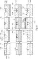
- Figures 6a to 6l illustrate a second part of a method of manufacturing the component carrier 100 according to an exemplary embodiment of the invention.
- the second method can directly build up on the first method and start with the product obtained in Figure 5h .
- a first magnetic element 150a is provided in form of a magnetic paste that is filled (poured) into the first cavity 135a by screen printing 163.
- a cavity can be formed by photo-imaging (when the dielectric layer structure 130 is a PID layer structure), etching, or by pre-cutting.
- a first magnetic element 150a is placed into the first cavity 135a, so that the first dielectric layer structure 130a surrounds the first magnetic element 150a.
- Figure 6b the stencil (for screen printing) 163 is removed and a first curing step is performed.
- Figure 6c overlapping magnetic material of the first magnetic element 150a is removed by grinding. A second curing step is performed.
- Figure 6d a plurality of gaps 156 are provided within the first magnetic element 150a (e.g. "laser trenching").
- a seed-layer 164 is provided (e.g. using electroless-plating and/or sputtering) to cover a respective bottoms of the plurality of gaps 156 and the upper main surface of the first dielectric layer structure 130a.
- Figure 6f the gaps 156 are filled by electro-plating 165, in particular with copper.
- the metal layer 165 on top of the upper main surface of the first part of the dielectric layer structure 130a is increased. Thereby, an electrically conductive structure 120 is formed in the gaps 156 in form of windings, so that an inductive element is provided.
- Figure 6h a second dielectric layer structure 130b is arranged (laminated) on the first PID layer structure 130a and the first magnetic element 150a.
- a second cavity 135b is formed within the second dielectric layer structure 130b as described for Figures 1a-c .
- Figure 6j after film layer removal, developing and curing the second dielectric layer structure 130b is done.
- the second cavity 135b is now arranged on top of the first magnetic element 150a and the embedded electrically conductive structure 120, whereby an upper main surface 151a of the first magnetic element 150a is exposed.
- Figure 6k a second magnetic element 150b is placed into the second cavity 135b (by screen printing), so that the second dielectric layer structure 130b surrounds the second magnetic element 150b.
- the second magnetic element 150b is placed directly on the first magnetic element 150a in order to embed the electrically conductive structure 120 within magnetic material.
- Figure 6l after removing of the stencil 163 that covers the dielectric layer structure 130, the following steps are performed: first curing, grinding, second curing. Then, the component carrier 100 described for Figure 1 is obtained.
Landscapes
- Engineering & Computer Science (AREA)
- Microelectronics & Electronic Packaging (AREA)
- Power Engineering (AREA)
- Manufacturing & Machinery (AREA)
- Coils Or Transformers For Communication (AREA)
Priority Applications (3)
| Application Number | Priority Date | Filing Date | Title |
|---|---|---|---|
| EP21174488.3A EP4093162A1 (de) | 2021-05-18 | 2021-05-18 | Komponententräger mit einem magnetischen element und herstellungsverfahren |
| US17/663,418 US12279372B2 (en) | 2021-05-18 | 2022-05-13 | Component carrier with a magnetic element and a manufacturing method |
| CN202210547379.2A CN115376780A (zh) | 2021-05-18 | 2022-05-18 | 具有磁性元件的部件承载件、制造方法以及光刻用途 |
Applications Claiming Priority (1)
| Application Number | Priority Date | Filing Date | Title |
|---|---|---|---|
| EP21174488.3A EP4093162A1 (de) | 2021-05-18 | 2021-05-18 | Komponententräger mit einem magnetischen element und herstellungsverfahren |
Publications (1)
| Publication Number | Publication Date |
|---|---|
| EP4093162A1 true EP4093162A1 (de) | 2022-11-23 |
Family
ID=76034431
Family Applications (1)
| Application Number | Title | Priority Date | Filing Date |
|---|---|---|---|
| EP21174488.3A Pending EP4093162A1 (de) | 2021-05-18 | 2021-05-18 | Komponententräger mit einem magnetischen element und herstellungsverfahren |
Country Status (3)
| Country | Link |
|---|---|
| US (1) | US12279372B2 (de) |
| EP (1) | EP4093162A1 (de) |
| CN (1) | CN115376780A (de) |
Families Citing this family (2)
| Publication number | Priority date | Publication date | Assignee | Title |
|---|---|---|---|---|
| WO2024151915A1 (en) * | 2023-01-12 | 2024-07-18 | Atlas Magentics | Method for increasing skin depth and reducing eddy currents in hybrid magnetic cores and composite metals using electroless plating techniques and resulting apparatus |
| CN119811892A (zh) * | 2024-12-26 | 2025-04-11 | 武汉大学 | 一种芯片感性元件的激光直写磁性薄膜封装方法 |
Citations (5)
| Publication number | Priority date | Publication date | Assignee | Title |
|---|---|---|---|---|
| EP1365451A1 (de) * | 2001-10-15 | 2003-11-26 | Matsushita Electric Industrial Co., Ltd. | Modulkomponente |
| US20060152321A1 (en) * | 2005-01-07 | 2006-07-13 | Samsung Electro-Mechanics Co., Ltd. | Planar magnetic inductor and method for manufacturing the same |
| DE102014209881A1 (de) * | 2014-05-23 | 2015-11-26 | Siemens Aktiengesellschaft | Mehrlagiges induktives passives Bauelement und Folienkörper zu dessen Herstellung |
| US20190304661A1 (en) * | 2018-03-28 | 2019-10-03 | Intel Corporation | Methods to selectively embed magnetic materials in substrate and corresponding structures |
| US20200005994A1 (en) * | 2018-06-27 | 2020-01-02 | Kyu-oh Lee | Substrate assembly with encapsulated magnetic feature |
Family Cites Families (24)
| Publication number | Priority date | Publication date | Assignee | Title |
|---|---|---|---|---|
| US6296955B1 (en) * | 1999-05-24 | 2001-10-02 | Read-Rite Corporation | High moment and high permeability transducer structures and formation |
| US7705411B2 (en) * | 2008-04-09 | 2010-04-27 | National Semiconductor Corporation | MEMS-topped integrated circuit with a stress relief layer |
| US8044755B2 (en) * | 2008-04-09 | 2011-10-25 | National Semiconductor Corporation | MEMS power inductor |
| US8305709B2 (en) * | 2008-08-08 | 2012-11-06 | Tdk Corporation | Perpendicular magnetic head and magnetic recording system having non-magnetic region in shield layer |
| US8300359B2 (en) * | 2009-12-30 | 2012-10-30 | Tdk Corporation | Perpendicular magnetic recording head and magnetic recording device |
| US8314676B1 (en) * | 2011-05-02 | 2012-11-20 | National Semiconductor Corporation | Method of making a controlled seam laminated magnetic core for high frequency on-chip power inductors |
| TW201311079A (zh) | 2011-08-19 | 2013-03-01 | Motech Ind Inc | 印刷用網布及其製造方法 |
| JP2014007339A (ja) * | 2012-06-26 | 2014-01-16 | Ibiden Co Ltd | インダクタ部品、その製造方法及びプリント配線板 |
| KR101933404B1 (ko) * | 2013-02-28 | 2018-12-28 | 삼성전기 주식회사 | 공통모드필터 및 이의 제조방법 |
| TWI570816B (zh) * | 2014-09-26 | 2017-02-11 | 矽品精密工業股份有限公司 | 封裝結構及其製法 |
| US20170092412A1 (en) * | 2015-09-26 | 2017-03-30 | Mathew J. Manusharow | Package integrated power inductors using lithographically defined vias |
| CN111066106B (zh) * | 2017-08-28 | 2023-04-04 | Tdk株式会社 | 线圈部件及其制造方法 |
| US11289263B2 (en) * | 2017-12-26 | 2022-03-29 | Intel Corporation | Electronic substrates having embedded magnetic material using photo-imagable dielectric layers |
| US11251113B2 (en) * | 2017-12-27 | 2022-02-15 | Intel Corporation | Methods of embedding magnetic structures in substrates |
| US11322444B2 (en) | 2018-03-23 | 2022-05-03 | Intel Corporation | Lithographic cavity formation to enable EMIB bump pitch scaling |
| EP3709779A1 (de) * | 2019-03-12 | 2020-09-16 | AT & S Austria Technologie & Systemtechnik Aktiengesellschaft | Komponententräger und verfahren zur herstellung davon |
| CN112351571B (zh) * | 2019-08-06 | 2022-08-16 | 奥特斯(中国)有限公司 | 半柔性部件承载件及其制造方法 |
| US11139239B2 (en) * | 2019-10-01 | 2021-10-05 | Taiwan Semiconductor Manufacturing Company, Ltd. | Recessed inductor structure to reduce step height |
| JP7180581B2 (ja) * | 2019-10-03 | 2022-11-30 | 株式会社村田製作所 | インダクタ部品及びインダクタ部品の製造方法 |
| US11335650B2 (en) * | 2020-06-11 | 2022-05-17 | Advanced Semiconductor Engineering, Inc. | Package substrate, electronic device package and method for manufacturing the same |
| US11322576B2 (en) * | 2020-07-29 | 2022-05-03 | Taiwan Semiconductor Manufacturing Company Limited | Inductive device |
| US12362295B2 (en) * | 2020-09-24 | 2025-07-15 | Intel Corporation | Planar magnetic radial inductors to enable VR disaggregation |
| US12272484B2 (en) * | 2021-03-04 | 2025-04-08 | Intel Corporation | Coreless electronic substrates having embedded inductors |
| US12334242B2 (en) * | 2021-03-11 | 2025-06-17 | Intel Corporation | Coreless electronic substrates having embedded inductors |
-
2021
- 2021-05-18 EP EP21174488.3A patent/EP4093162A1/de active Pending
-
2022
- 2022-05-13 US US17/663,418 patent/US12279372B2/en active Active
- 2022-05-18 CN CN202210547379.2A patent/CN115376780A/zh active Pending
Patent Citations (5)
| Publication number | Priority date | Publication date | Assignee | Title |
|---|---|---|---|---|
| EP1365451A1 (de) * | 2001-10-15 | 2003-11-26 | Matsushita Electric Industrial Co., Ltd. | Modulkomponente |
| US20060152321A1 (en) * | 2005-01-07 | 2006-07-13 | Samsung Electro-Mechanics Co., Ltd. | Planar magnetic inductor and method for manufacturing the same |
| DE102014209881A1 (de) * | 2014-05-23 | 2015-11-26 | Siemens Aktiengesellschaft | Mehrlagiges induktives passives Bauelement und Folienkörper zu dessen Herstellung |
| US20190304661A1 (en) * | 2018-03-28 | 2019-10-03 | Intel Corporation | Methods to selectively embed magnetic materials in substrate and corresponding structures |
| US20200005994A1 (en) * | 2018-06-27 | 2020-01-02 | Kyu-oh Lee | Substrate assembly with encapsulated magnetic feature |
Also Published As
| Publication number | Publication date |
|---|---|
| CN115376780A (zh) | 2022-11-22 |
| US20220377896A1 (en) | 2022-11-24 |
| US12279372B2 (en) | 2025-04-15 |
Similar Documents
| Publication | Publication Date | Title |
|---|---|---|
| US11324122B2 (en) | Component carrier and method of manufacturing the same | |
| US20210337653A1 (en) | Component Carrier With an Embedded Thermally Conductive Block and Manufacturing Method | |
| US12136580B2 (en) | Embedding methods for fine-pitch components and corresponding component carriers | |
| US12279372B2 (en) | Component carrier with a magnetic element and a manufacturing method | |
| US12495498B2 (en) | Component carrier interconnection and manufacturing method | |
| US11882648B2 (en) | Dielectric layer for component carrier with varying material properties | |
| US11551989B2 (en) | Component carrier and method of manufacturing the same | |
| US20220377897A1 (en) | Magnetic Inlay With Electrically Conductive Vertical Through Connections for a Component Carrier | |
| US20230298808A1 (en) | Inductor Inlay for a Component Carrier and a Method of Manufacturing the Same | |
| US12464649B2 (en) | Component carrier with inductive element included in layer build-up, and manufacturing method | |
| US20220377917A1 (en) | Component Carrier With Magnetic Element, Magnetic Inlay, and Manufacturing Method | |
| US12543267B2 (en) | Magnetic inlay with an adjustable inductance value for a component carrier and a manufacturing method | |
| EP4192209A1 (de) | Verfahren zur herstellung eines komponententrägers und komponententräger | |
| US20250300060A1 (en) | Component Carrier, Component Carrier Arrangement and Method of Manufacturing the Component Carrier | |
| US20260123409A1 (en) | Component Carrier With Protruding Thermal Structure and Manufacture Method | |
| US20250301570A1 (en) | Component Carrier and Method Manufacturing the Component Carrier | |
| US11412618B2 (en) | Component carrier and method of manufacturing the same | |
| US20250267786A1 (en) | Component carrier with flexible portions and manufacturing method | |
| WO2024115565A1 (en) | Component carrier with reinforcing portion, and manufacture method | |
| WO2025195689A1 (en) | Component carrier and method for manufacturing the component carrier |
Legal Events
| Date | Code | Title | Description |
|---|---|---|---|
| PUAI | Public reference made under article 153(3) epc to a published international application that has entered the european phase |
Free format text: ORIGINAL CODE: 0009012 |
|
| STAA | Information on the status of an ep patent application or granted ep patent |
Free format text: STATUS: THE APPLICATION HAS BEEN PUBLISHED |
|
| AK | Designated contracting states |
Kind code of ref document: A1 Designated state(s): AL AT BE BG CH CY CZ DE DK EE ES FI FR GB GR HR HU IE IS IT LI LT LU LV MC MK MT NL NO PL PT RO RS SE SI SK SM TR |
|
| STAA | Information on the status of an ep patent application or granted ep patent |
Free format text: STATUS: REQUEST FOR EXAMINATION WAS MADE |
|
| 17P | Request for examination filed |
Effective date: 20230427 |
|
| RBV | Designated contracting states (corrected) |
Designated state(s): AL AT BE BG CH CY CZ DE DK EE ES FI FR GB GR HR HU IE IS IT LI LT LU LV MC MK MT NL NO PL PT RO RS SE SI SK SM TR |