EP4095512A1 - Plaque arrière de canal microfluidique et son procédé de fabrication, et puce de détection microfluidique - Google Patents
Plaque arrière de canal microfluidique et son procédé de fabrication, et puce de détection microfluidique Download PDFInfo
- Publication number
- EP4095512A1 EP4095512A1 EP20891412.7A EP20891412A EP4095512A1 EP 4095512 A1 EP4095512 A1 EP 4095512A1 EP 20891412 A EP20891412 A EP 20891412A EP 4095512 A1 EP4095512 A1 EP 4095512A1
- Authority
- EP
- European Patent Office
- Prior art keywords
- channel
- microfluidic
- sample
- sub
- channels
- Prior art date
- Legal status (The legal status is an assumption and is not a legal conclusion. Google has not performed a legal analysis and makes no representation as to the accuracy of the status listed.)
- Pending
Links
Images




Classifications
-
- B—PERFORMING OPERATIONS; TRANSPORTING
- B01—PHYSICAL OR CHEMICAL PROCESSES OR APPARATUS IN GENERAL
- B01L—CHEMICAL OR PHYSICAL LABORATORY APPARATUS FOR GENERAL USE
- B01L3/00—Containers or dishes for laboratory use, e.g. laboratory glassware; Droppers
- B01L3/50—Containers for the purpose of retaining a material to be analysed, e.g. test tubes
- B01L3/502—Containers for the purpose of retaining a material to be analysed, e.g. test tubes with fluid transport, e.g. in multi-compartment structures
- B01L3/5027—Containers for the purpose of retaining a material to be analysed, e.g. test tubes with fluid transport, e.g. in multi-compartment structures by integrated microfluidic structures, i.e. dimensions of channels and chambers are such that surface tension forces are important, e.g. lab-on-a-chip
- B01L3/502715—Containers for the purpose of retaining a material to be analysed, e.g. test tubes with fluid transport, e.g. in multi-compartment structures by integrated microfluidic structures, i.e. dimensions of channels and chambers are such that surface tension forces are important, e.g. lab-on-a-chip characterised by interfacing components, e.g. fluidic, electrical, optical or mechanical interfaces
-
- B—PERFORMING OPERATIONS; TRANSPORTING
- B01—PHYSICAL OR CHEMICAL PROCESSES OR APPARATUS IN GENERAL
- B01L—CHEMICAL OR PHYSICAL LABORATORY APPARATUS FOR GENERAL USE
- B01L3/00—Containers or dishes for laboratory use, e.g. laboratory glassware; Droppers
- B01L3/50—Containers for the purpose of retaining a material to be analysed, e.g. test tubes
- B01L3/502—Containers for the purpose of retaining a material to be analysed, e.g. test tubes with fluid transport, e.g. in multi-compartment structures
- B01L3/5027—Containers for the purpose of retaining a material to be analysed, e.g. test tubes with fluid transport, e.g. in multi-compartment structures by integrated microfluidic structures, i.e. dimensions of channels and chambers are such that surface tension forces are important, e.g. lab-on-a-chip
- B01L3/502707—Containers for the purpose of retaining a material to be analysed, e.g. test tubes with fluid transport, e.g. in multi-compartment structures by integrated microfluidic structures, i.e. dimensions of channels and chambers are such that surface tension forces are important, e.g. lab-on-a-chip characterised by the manufacture of the container or its components
-
- B—PERFORMING OPERATIONS; TRANSPORTING
- B01—PHYSICAL OR CHEMICAL PROCESSES OR APPARATUS IN GENERAL
- B01L—CHEMICAL OR PHYSICAL LABORATORY APPARATUS FOR GENERAL USE
- B01L3/00—Containers or dishes for laboratory use, e.g. laboratory glassware; Droppers
- B01L3/50—Containers for the purpose of retaining a material to be analysed, e.g. test tubes
- B01L3/502—Containers for the purpose of retaining a material to be analysed, e.g. test tubes with fluid transport, e.g. in multi-compartment structures
- B01L3/5027—Containers for the purpose of retaining a material to be analysed, e.g. test tubes with fluid transport, e.g. in multi-compartment structures by integrated microfluidic structures, i.e. dimensions of channels and chambers are such that surface tension forces are important, e.g. lab-on-a-chip
- B01L3/50273—Containers for the purpose of retaining a material to be analysed, e.g. test tubes with fluid transport, e.g. in multi-compartment structures by integrated microfluidic structures, i.e. dimensions of channels and chambers are such that surface tension forces are important, e.g. lab-on-a-chip characterised by the means or forces applied to move the fluids
-
- G—PHYSICS
- G01—MEASURING; TESTING
- G01N—INVESTIGATING OR ANALYSING MATERIALS BY DETERMINING THEIR CHEMICAL OR PHYSICAL PROPERTIES
- G01N15/00—Investigating characteristics of particles; Investigating permeability, pore-volume or surface-area of porous materials
- G01N15/02—Investigating particle size or size distribution
-
- B—PERFORMING OPERATIONS; TRANSPORTING
- B01—PHYSICAL OR CHEMICAL PROCESSES OR APPARATUS IN GENERAL
- B01L—CHEMICAL OR PHYSICAL LABORATORY APPARATUS FOR GENERAL USE
- B01L2200/00—Solutions for specific problems relating to chemical or physical laboratory apparatus
- B01L2200/16—Reagents, handling or storing thereof
-
- B—PERFORMING OPERATIONS; TRANSPORTING
- B01—PHYSICAL OR CHEMICAL PROCESSES OR APPARATUS IN GENERAL
- B01L—CHEMICAL OR PHYSICAL LABORATORY APPARATUS FOR GENERAL USE
- B01L2300/00—Additional constructional details
- B01L2300/04—Closures and closing means
- B01L2300/041—Connecting closures to device or container
-
- B—PERFORMING OPERATIONS; TRANSPORTING
- B01—PHYSICAL OR CHEMICAL PROCESSES OR APPARATUS IN GENERAL
- B01L—CHEMICAL OR PHYSICAL LABORATORY APPARATUS FOR GENERAL USE
- B01L2300/00—Additional constructional details
- B01L2300/06—Auxiliary integrated devices, integrated components
- B01L2300/0627—Sensor or part of a sensor is integrated
- B01L2300/0645—Electrodes
-
- B—PERFORMING OPERATIONS; TRANSPORTING
- B01—PHYSICAL OR CHEMICAL PROCESSES OR APPARATUS IN GENERAL
- B01L—CHEMICAL OR PHYSICAL LABORATORY APPARATUS FOR GENERAL USE
- B01L2300/00—Additional constructional details
- B01L2300/08—Geometry, shape and general structure
- B01L2300/0809—Geometry, shape and general structure rectangular shaped
- B01L2300/0819—Microarrays; Biochips
-
- B—PERFORMING OPERATIONS; TRANSPORTING
- B01—PHYSICAL OR CHEMICAL PROCESSES OR APPARATUS IN GENERAL
- B01L—CHEMICAL OR PHYSICAL LABORATORY APPARATUS FOR GENERAL USE
- B01L2300/00—Additional constructional details
- B01L2300/08—Geometry, shape and general structure
- B01L2300/0887—Laminated structure
-
- B—PERFORMING OPERATIONS; TRANSPORTING
- B01—PHYSICAL OR CHEMICAL PROCESSES OR APPARATUS IN GENERAL
- B01L—CHEMICAL OR PHYSICAL LABORATORY APPARATUS FOR GENERAL USE
- B01L2400/00—Moving or stopping fluids
- B01L2400/04—Moving fluids with specific forces or mechanical means
- B01L2400/0403—Moving fluids with specific forces or mechanical means specific forces
- B01L2400/0415—Moving fluids with specific forces or mechanical means specific forces electrical forces, e.g. electrokinetic
Definitions
- the present disclosure relates to the field of microfluidic technologies, and in particular, to a microfluidic channel backplane and a method of manufacturing the same, and a microfluidic detection chip.
- Microfluidic technology refers to a technology for processing or manipulating a minute amount of fluid (nanoliter (nL) to microliter ( ⁇ L) in volume) by using microchannels (tens to hundreds of microns in size).
- a microfluidic chip is a main platform to realize the microfluidic technology.
- the microfluidic chip has characteristics of parallel sample collection and processing, high integration, high-throughput, high analysis speed, low power consumption, low material consumption, low pollution, etc.
- the microfluidic chip technology may be applied to fields such as biological genetic engineering, disease diagnosis and drug research, cell analysis, environmental monitoring and protection, health quarantine and judicial identification. In recent years, the microfluidic chip technology has been rapidly developed.
- the microfluidic chip is a hot spot field of current development of a miniaturized total analysis system.
- a microfluidic channel backplane in one aspect, includes a base, and a plurality of microfluidic channels, a sample-adding channel and an enrichment channel that are disposed above the base.
- Each microfluidic channel of the plurality of microfluidic channels includes a first end and a second end.
- the sample-adding channel is communicated with first ends of the plurality of microfluidic channels.
- the enrichment channel includes a first enrichment sub-channel and a second enrichment sub-channel.
- the first enrichment sub-channel is communicated with second ends of the plurality of microfluidic channels, and one end of the second enrichment sub-channel is communicated with the first enrichment sub-channel.
- the sample-adding channel includes a first sample-adding sub-channel and at least two second sample-adding sub-channels.
- One side of the first sample-adding sub-channel is communicated with the first ends of the plurality of microfluidic channels, and another side of the first sample-adding sub-channel is communicated with one side of each second sample-adding sub-channel of the at least two second sample-adding sub-channels.
- a dimension of the first sample-adding sub-channel in a first direction is greater than a dimension of each second sample-adding sub-channel of the at least two second sample-adding sub-channels in the first direction.
- the first direction is parallel to a direction in which the plurality of microfluidic channels are arranged.
- the at least two second sample-adding sub-channels are spaced apart and arranged in parallel in the first direction.
- the sample-adding channel includes two second sample-adding sub-channels.
- the two second sample-adding sub-channels and the first sample-adding sub-channel are arranged in a U shape.
- the first enrichment sub-channel extends in a first direction, and the first direction is parallel to a direction in which the plurality of microfluidic channels are arranged.
- the second enrichment sub-channel extends in a second direction. The second direction is parallel to an extending direction of each microfluidic channel.
- the first enrichment sub-channel and the second enrichment sub-channel are arranged in an L shape or a T shape.
- the microfluidic channel backplane further includes a microfluidic channel layer disposed on the base, and a supporting layer disposed on a side of the microfluidic channel layer away from the base.
- the plurality of microfluidic channels are disposed in the microfluidic channel layer.
- a first depression, a second depression, and a plurality of supporting columns located in the first depression and the second depression are formed in the supporting layer, and the plurality of supporting columns have gaps therebetween.
- the first depression and gaps between supporting columns located in the first depression constitute the sample-adding channel.
- the second depression and gaps between supporting columns located in the second depression constitute the enrichment channel.
- a first communication opening is provided on a side of the first ends of the plurality of microfluidic channels away from the base, and the first communication opening is configured such that the first ends of the plurality of microfluidic channels are communicated with the sample-adding channel.
- a second communication opening is provided on a side of the second ends of the plurality of microfluidic channels away from the base, and the second communication opening is configured such that the second ends of the plurality of microfluidic channels are communicated with the first enrichment sub-channel of the enrichment channel.
- the first communication opening and the second communication opening extend in a first direction, and the first direction is parallel to a direction in which the plurality of microfluidic channels are arranged.
- each microfluidic channel of the plurality of microfluidic channels is of an integrally formed structure.
- the microfluidic channel backplane further includes a foundation layer disposed on a side of the microfluidic channel layer proximate to the base.
- the foundation layer includes a plurality of grooves, and at least one groove of the plurality of grooves having at least one microfluidic channel of the plurality of microfluidic channels formed thereover.
- the microfluidic channel backplane further includes a bonding film layer disposed on a side of the supporting layer away from the base.
- the bonding film layer is configured such that the microfluidic channel backplane is bonded to a cover plate.
- the microfluidic channel backplane further includes a control electrode disposed at a side of the plurality of microfluidic channels proximate to or away from the base.
- An orthogonal projection of the control electrode on the base is at least partially overlapped with an orthogonal projection of each microfluidic channel of the plurality of microfluidic channels on the base.
- the control electrode is configured to transmit a control signal to control an enrichment rate of microfluid flowing through the plurality of microfluidic channels.
- control electrode extends in a first direction, and the first direction is parallel to a direction in which the plurality of microfluidic channels are arranged.
- the microfluidic channel backplane further includes a driving electrode disposed at a side of the plurality of microfluidic channels proximate to or away from the base.
- An orthogonal projection of the driving electrode on the base is at least partially overlapped with an orthogonal projection of the sample-adding channel on the base.
- the driving electrode is configured to transmit a first driving signal to form an electric field for driving movement of microfluid.
- microfluidic detection chip in another aspect, includes the microfluidic channel backplane as described in any of the above embodiments, and a cover plate arranged opposite to the microfluidic channel backplane.
- the cover plate is provided with two sample-adding openings therein, and the two sample-adding openings are communicated with the two second sample-adding sub-channels, respectively.
- the cover plate includes a detection channel arranged in a U shape, and the detection channel is communicated with an end, away from the first enrichment sub-channel, of the second enrichment sub-channel of the enrichment channel in the microfluidic channel backplane.
- the cover plate is provided with two detection openings therein, and the two detection openings are respectively disposed at two ends of the detection channel and are communicated with the detection channel.
- the two detection openings are configured to be coupled to an external detection device, so as to apply a second driving signal to microfluid flowing through the detection channel, and are configured to cooperate with a driving electrode in the microfluidic channel backplane to which a first driving signal is applied to form an electric field for driving movement of the microfluid.
- a method of manufacturing a microfluidic channel backplane includes: providing a base, and forming a microfluidic channel film on a side of the base, the microfluidic channel film being formed with a plurality of microfluidic channels therein, and each microfluidic channel of the plurality of microfluidic channels including a first end and a second end; forming a supporting film on a side of the microfluidic channel film away from the base; patterning the supporting film to form a first depression, a second depression, and a plurality of supporting columns located in the first depression and the second depression; the first depression and gaps between supporting columns located in the first depression forming a sample-adding channel, and the second depression and gaps between supporting columns located in the second depression forming an enrichment channel; the enrichment channel including a first enrichment sub-channel and a second enrichment sub-channel that are communicated with each other; and etching the microfluidic channel film downwards to form a first communication opening
- the manufacturing method further includes: forming a conductive film on a side of the microfluidic channel film away from the base after forming the microfluidic channel film and before forming the support film; patterning the conductive film to form a control electrode and a driving electrode.
- An orthogonal projection of the control electrode on the base is at least partially overlapped with an orthogonal projection of each microfluidic channel of the plurality of microfluidic channels on the base; and an orthogonal projection of the driving electrode on the base is at least partially overlapped with an orthogonal projection of the sample-adding channel on the base.
- forming the microfluidic channel film that is formed with the plurality of microfluidic channels therein on the side of the base includes: forming a foundation layer including a plurality of grooves on a side of the base; and depositing a microfluidic channel film material on a side of the foundation layer away from the base, a microfluidic channel being integrally formed over each groove of the plurality of grooves during a deposition process.
- first and second are only used for descriptive purposes, and are not to be construed as indicating or implying the relative importance or implicitly indicating the number of indicated technical features. Thus, features defined by “first” and “second” may explicitly or implicitly include one or more of the features. In the description of the embodiments of the present disclosure, "a plurality of/the plurality of” means two or more unless otherwise specified.
- Coupled In the description of some embodiments, terms “coupled”, “connected” and their derivatives may be used. For example, term “connected” may be used in the description of some embodiments to indicate that two or more components are in direct physical or electric contact with each other. For another example, term “coupled” may be used in the description of some embodiments to indicate that two or more components are in direct physical or electric contact. However, term “coupled” or “communicatively coupled” may also mean that two or more components are not in direct contact with each other, but still cooperate or interact with each other. The embodiments disclosed herein are not necessarily limited to the contents herein.
- phrases "at least one of A, B and C” has a same meaning as the phrase "at least one of A, B or C", and they both include the following combinations of A, B and C: only A, only B, only C, a combination of A and B, a combination of A and C, a combination of B and C, and a combination of A, B and C.
- a and/or B includes the following three combinations: only A, only B, and a combination of A and B.
- Microfluidic technology may integrate basic operation units for sample reaction, separation and detection in a biological, chemical or medical analysis process into a micron-scale chip to manufacture a microfluidic detection chip.
- the microfluidic detection chip is used for controlling a sample to be detected, so as to realize detection of the sample to be detected.
- some embodiments of the present disclosure provide a microfluidic channel backplane 1A, and a microfluidic detection chip 3A that includes the microfluidic channel backplane 1A.
- the microfluidic detection chip 3A may enrich a concentration of molecules to be detected in a sample to be detected before detecting the sample to be detected, so as to improve a detection precision of the sample to be detected.
- the sample to be detected may be a liquid substance, for example, a blood sample.
- the molecules to be detected in the blood sample may be, for example, hemoglobin, platelets, pathogenic cells, or the like.
- the microfluidic channel backplane 1A includes a base 1, and a plurality of microfluidic channels 21, a sample-adding channel 31 and an enrichment channel 32 that are disposed above the base 1.
- the base 1 may be a glass substrate, a quartz substrate, a silicon substrate, or the like.
- each microfluidic channel of the plurality of microfluidic channels 21 includes a first end 211 and a second end 212.
- the sample-adding channel 31 is communicated with first ends 211 of the plurality of microfluidic channels 21.
- the enrichment channel 32 includes a first enrichment sub-channel 321 and a second enrichment sub-channel 322.
- the first enrichment sub-channel 321 is communicated with second ends 212 of the plurality of microfluidic channels 21.
- One end of the second enrichment sub-channel 322 is communicated with the first enrichment sub-channel 321.
- the plurality of microfluidic channels 21 are arranged in an array to form a microfluidic channel array.
- the plurality of microfluidic channels 21 are arranged in parallel in a first direction D1, and each microfluidic channel 21 extends in a second direction D2.
- the first direction D1 and the second direction D2 intersect.
- the first direction D1 and the second direction D2 are perpendicular to each other.
- each microfluidic channel 21 of the plurality of microfluidic channels 21 is a nano-scale channel. That is, a pore diameter of each microfluidic channel 21 is less than 1000 nm.
- the pore diameter of each microfluidic channel 21 may be in a range from approximately 1 nm to approximately 50 nm, or in a range from approximately 50 nm to approximately 100 nm, or in a range from approximately 100 nm to approximately 1000 nm.
- the pore diameter may refer to a minimum pore diameter or an average pore diameter of the microfluidic channel 21.
- the microfluidic channel 21 is the nano-scale channel
- layers in an electric double layer at the inner wall of the microfluidic channel 21 are overlapped with each other in the channel. Substances with the same charge property as the electric double layer cannot pass through the channel, whereas substances with opposite charges or neutral substances may pass through the channel. That is, there is a charge repulsion enrichment mechanism. Therefore, the microfluidic channel 21 in the microfluidic channel backplane 1A provided in the above embodiments may realize enrichment of sample molecule concentration by utilizing the charge repulsion enrichment mechanism.
- the sample-adding channel 31 and the enrichment channel 32 are disposed at a side of the plurality of microfluidic channels 21 away from the base 1.
- the sample-adding channel 31 is communicated with the first ends 211 of the plurality of microfluidic channels 21.
- the sample-adding channel 31 is used in a way that a sample to be detected with a lower concentration is added into the microfluidic channel backplane 1A through it, and is used for transporting the sample to be detected with the lower concentration to the first ends 211 of the plurality of microfluidic channels 21.
- the enrichment channel 32 is communicated with the second ends 212 of the plurality of microfluidic channels 21, and the enrichment channel 32 is used for receiving a sample to be detected with a higher concentration obtained after enrichment through the plurality of microfluidic channels 21.
- the sample-adding channel 31 of the microfluidic channel backplane 1A provided in the above embodiments is communicated with the first ends 211 of the plurality of microfluidic channels 21, and the first enrichment sub-channel 321 is communicated with the second ends 212 of the plurality of microfluidic channels 21.
- the plurality of microfluidic channels 21 have selectivity for the molecules to be detected in the sample to be detected, that is, only the molecules to be detected in the sample to be detected are allowed to pass.
- a concentration of the molecules to be detected in the sample to be detected is lower at the first ends 211 of the plurality of microfluidic channels 21, and is increased at the second ends 212 of the plurality of microfluidic channels 21. In this way, the concentration of the sample to be detected is higher in the first enrichment sub-channel 321.
- one end of the second enrichment sub-channel 322 of the microfluidic channel backplane 1A provided in the above embodiments is communicated with the first enrichment sub-channel 321, so that the sample to be detected with the higher concentration enriched in the first enrichment sub-channel 321 gathers in the second enrichment sub-channel 322 to be detected more easily.
- the sample-adding channel 31 includes a first sample-adding sub-channel 311 and at least two second sample-adding sub-channels 312.
- One side of the first sample-adding sub-channel 311 is communicated with the first ends 211 of the plurality of microfluidic channels 21, and another side of the first sample-adding sub-channel 311 is communicated with one side of each second sample-adding sub-channel 312 of the at least two second sample-adding sub-channels 312.
- a dimension of the first sample-adding sub-channel 311 in the first direction D1 is greater than a dimension of each second sample-adding sub-channel 312 of the at least two second sample-adding sub-channels 312 in the first direction D1 (referring to d 2 and d 3 shown in FIG. 1 ).
- the at least two second sample-adding sub-channels 312 are spaced apart and arranged in parallel in the first direction D1.
- the sample to be detected when the sample to be detected is added into the sample-adding channel 31, the sample to be detected may be added into any one or some of the at least two second sample-adding sub-channels 312, and remaining second sample-adding sub-channel(s) are used as exhaust channel(s). In this way, bubbles may be prevented from generating in the sample to be detected, thereby avoiding blockage of the plurality of microfluidic channels 21.
- the sample-adding channel 31 includes two second sample-adding sub-channels 312.
- the two second sample-adding sub-channels 312 and the first sample-adding sub-channel 311 are arranged in a U shape.
- one second sample-adding sub-channel 312 of the two second sample-adding sub-channels 312 is used for addition of the sample to be detected, and the other second sample-adding sub-channel 312 is used as an exhaust channel.
- the two sample-adding sub-channels 312 are spaced apart and arranged in parallel.
- the dimension of the first sample-adding sub-channel 311 in the first direction D1 is equal to d 1 .
- Dimensions of the two second sample-adding sub-channel 312 in the first direction D1 are d 2 and d 3 , respectively.
- d 1 is greater than d 2 and d 1 is greater than d 3 .
- the sample to be detected when the sample to be detected is added into the sample-adding channel 31, the sample to be detected may be added into one second sample-adding sub-channel 312 of the two second sample-adding sub-channels 312, and the other second sample-adding sub-channel 312 may be used as an exhaust channel.
- bubbles may be prevented from generating in the sample to be detected, thereby avoiding blockage of the plurality of microfluidic channels 21.
- the first enrichment sub-channel 321 extends in the first direction D1
- the second enrichment sub-channel 322 extends in the second direction D2.
- the first direction D1 is parallel to a direction in which the plurality of microfluidic channels 21 are arranged
- the second direction D2 is parallel to an extending direction of each microfluidic channel 21. This facilitates communication between the first enrichment sub-channel 321 and each microfluidic channel 21.
- the second enrichment sub-channel 322 extends in a direction away from the first enrichment sub-channel 321 to facilitate communication between the first enrichment sub-channel 321 and a detection channel 72 in the backplane 2A.
- the first enrichment sub-channel 321 and the second enrichment sub-channel 322 are arranged in an L shape. That is, one end of the second enrichment sub-channel 322 is communicated with one end of the first enrichment sub-channel 321.
- the arrangement form is simple in structure and easy to realize.
- the first enrichment sub-channel 321 and the second enrichment sub-channel 322 are arranged in a T shape. That is, one end of the second enrichment sub-channel 322 is communicated with a middle portion of the first enrichment sub-channel 321 (a position other than both ends of the first enrichment sub-channel 321).
- the microfluidic channel backplane 1A provided in embodiments of the present disclosure further includes a control electrode 61 disposed at a side of the plurality of microfluidic channels 21 proximate to or away from the base 1.
- An orthogonal projection of the control electrode 61 on the base 1 is at least partially overlapped with an orthogonal projection of each microfluidic channel 21 of the plurality of microfluidic channels 21 on the base 1.
- the control electrode 61 is configured to transmit a control signal to control an enrichment rate of microfluid flowing through the plurality of microfluidic channels 21.
- the control electrode 61 is connected to a gate voltage VG, and an amount of charge on the plurality of microfluidic channels 21 is controlled by adjusting a magnitude of the gate voltage VG.
- the enrichment rate of the microfluid flowing through the plurality of microfluidic channels 21 is controlled according to a principle that unlike charges attract and like charges repel.
- the plurality of microfluidic channels 21 have positive charges
- the sample molecules to be detected have negative charges
- the enrichment rate of the sample molecules to be detected is increased by increasing the amount of charge in the plurality of microfluidic channels 21.
- the plurality of microfluidic channels 21 are arranged in the array, a direction parallel to the direction in which the plurality of microfluidic channels 21 are arranged is the first direction D1, and the extending direction of the plurality of microfluidic channels 21 is the second direction D2.
- the control electrode 61 extends in the first direction D1. That is, the control electrode 61 is parallel to the direction in which the plurality of microfluidic channels 21 are arranged, and spans the plurality of microfluidic channels 21.
- the control electrode 61 has a signal access terminal 611, and the signal access terminal 611 is used for receiving a control signal (e.g., a voltage signal).
- a dimension of the signal access terminal 611 in the second direction D2 may be greater than a dimension of the control electrode 61 in the second direction D2, which facilitates a connection between the signal access terminal 611 and an external device for providing the control signal.
- the microfluidic channel backplane 1A provided in the embodiments of the present disclosure further includes a driving electrode 62 disposed at a side of the plurality of microfluidic channels 21 proximate to or away from the base 1.
- An orthogonal projection of the driving electrode 62 on the base 1 is at least partially overlapped with an orthogonal projection of the sample-adding channel 31 on the base 1.
- the driving electrode 62 is configured to transmit a first driving signal to form an electric field for driving movement of microfluid.
- the first driving signal received by the driving electrode 62 is a first potential signal.
- the first potential signal is, for example, a ground potential signal or any other constant potential signal.
- Materials of the control electrode 61 and the driving electrode 62 include any one of indium tin oxide, molybdenum, aluminum, copper, and other conductive materials. Of course, the materials of the control electrode 61 and the driving electrode 62 are not limited to the above materials, and are not limited herein.
- control electrode 61 and the driving electrode 62 may be made of the same material or different materials, and may be disposed in the same layer or different layers.
- the microfluidic channel backplane 1A provided in embodiments of the present disclosure further includes a detection unit 8.
- the detection unit 8 is arranged proximate to the second enrichment sub-channel 322.
- the detection unit 8 includes an optical sensor capable of converting a received optical signal into a corresponding electrical signal.
- the electrical signal may be analyzed to obtain a property of the sample to be detected.
- the detection unit 8 is not limited to an optical sensor, and it may also be other sensors, which will not be listed herein.
- microfluidic channel backplane 1A The above are exemplary descriptions of components or structures included in the microfluidic channel backplane 1A. Based on one or more of the above embodiments, a film structure of the microfluidic channel backplane 1A will be exemplarily described below.
- the microfluidic channel backplane 1A includes a microfluidic channel layer 2 disposed on the base 1, and the plurality of microfluidic channels 21 are disposed in the microfluidic channel layer 2.
- each microfluidic channel 21 of the plurality of microfluidic channels 21 is of an integrally formed structure.
- the microfluidic channel backplane 1A provided in embodiments of the present disclosure further includes a foundation layer 4 disposed on a side of the microfluidic channel layer 2 proximate to the base 1.
- the foundation layer 4 includes a plurality of grooves 41, and at least one groove 41 of the plurality of grooves 41 has at least one microfluidic channel 21 of the plurality of microfluidic channels 21 formed thereover.
- the foundation layer 4 may be formed through a patterning technique such as ultraviolet exposure, electron beam exposure, nano-imprinting, photolithographic stripping, etc.
- the foundation layer 4 may also be formed through the above patterning technique in combination with a processing technique such as dry etching, hot corrosion, etc.
- the plurality of microfluidic channels 21 may be obtained through a deposition process.
- a requirement for a process precision of the plurality of grooves 41 in the foundation layer 4 is low.
- the plurality of microfluidic channels 21 with a high process precision are formed on the foundation layer 4 with a relatively low process precision through the deposition process, so that a requirement for a patterning precision of a device is decreased.
- microfluidic channel layer 2 and the plurality of microfluidic channels 21 are formed by natural growth through the deposition process, but not by etching. Therefore, defects caused by etching uniformity may be avoided, and there is no need to develop different etching processes for different deposition materials.
- the closed channels may be formed without attaching a backplane with a cover plate, which avoids the attaching difficulty and improves the quality of the microfluidic channels.
- a first communication opening 211a is provided on a side of the first ends 211 of the plurality of microfluidic channels 21 away from the base 1.
- the first communication opening 211a is configured such that the first ends 221 of the plurality of microfluidic channels 21 are communicated with the sample-adding channel 31. That is, the sample-adding channel 31 is communicated with the first ends 221 of the plurality of microfluidic channels 21 through the first communication opening 211a.
- an order of magnitude of a dimension of the sample-adding channel 31 and an order of magnitude of a dimension of the first communication opening 211a are both greater than an order of magnitude of a dimension of each microfluidic channel 21 of the plurality of microfluidic channels 21.
- the order of magnitude of the dimension of the sample-adding channel 31 and the order of magnitude of the dimension of the first communication opening 211a are both an order of micrometers (greater than 1 ⁇ m), and the order of magnitude of the dimension of each microfluidic channel 21 of the plurality of microfluidic channels 21 is an order of nanometers (less than 1 ⁇ m).
- the sample-adding channel 31 is communicated with the first ends 211 of the plurality of microfluidic channels 21 through the first communication opening 211a. Based on this, as long as a communication between the sample-adding channel 31 and the first communication opening 211a is realized, a communication between the sample-adding channel 31 and each microfluidic channel 21 of the plurality of microfluidic channels 21 is realized, which reduces the alignment difficulty between the sample-adding channel 31 and the plurality of microfluidic channels 21 in a communication process.
- a second communication opening 212a is provided on a side of the second ends 212 of the plurality of microfluidic channels 21 away from the base 1.
- the second communication opening 212a is configured such that the second ends 212 of the plurality of microfluidic channels 21 are communicated with the first enrichment sub-channel 321 of the enrichment channel 32. That is, the first enrichment sub-channel 321 is communicated with the second ends 212 of the plurality of microfluidic channels 21 through the second communication opening 212a.
- an order of magnitude of a dimension of the first enrichment sub-channel 321 and an order of magnitude of a dimension of the second communication opening 212a are both greater than the order of magnitude of the dimension of each microfluidic channel 21 of the plurality of microfluidic channels 21.
- the order of magnitude of the dimension of the first enrichment sub-channel 321 and the order of magnitude of the dimension of the second communication opening 212a are both an order of micrometers (greater than 1 ⁇ m), and the order of magnitude of the dimension of each microfluidic channel 21 of the plurality of microfluidic channels 21 is an order of nanometers.
- the first enrichment sub-channel 321 is communicated with the second ends 212 of the plurality of microfluidic channels 21 through the second communication opening 212a. Based on this, as long as a communication between the first enrichment sub-channel 321 and the second communication opening 212a is realized, a communication between the first enrichment sub-channel 321 and each microfluidic channel 21 of plurality of microfluidic channels 21 is realized, which reduces the alignment difficulty between the first enrichment sub-channel 321 and the plurality of microfluidic channels 21 in a communication process.
- the microfluidic channel backplane 1A provided in embodiments of the present disclosure further includes a supporting layer 3 disposed on a side of the microfluidic channel layer 2 away from the base 1.
- the supporting layer 3 may be used for supporting the cover plate 2A, so as to prevent the microfluidic channel layer 2 from collapsing and damaging a structure of the plurality of microfluidic channels 21.
- a first depression 33, a second depression 34, and a plurality of supporting columns 35 located in the first depression 33 and the second depression 34 are formed in the supporting layer 3. There are gaps 36 between the plurality of supporting columns 35.
- the first depression 33 and gaps 36 between supporting columns 35 located in the first depression 33 form the sample-adding channel 31.
- the second depression 34 and gaps 36 between supporting columns 35 located in the second depression 34 form the enrichment channel 32.
- the sample to be detected moves to the first communication opening 211a through the gaps 36 between the supporting columns 35. Then, the molecules to be detected in the sample to be detected flow through the plurality of microfluidic channels 21 from the first communication opening 211a to the second communication opening 212a, during which the molecules to be detected are enriched. Then, the molecules to be detected enter the second depression 34.
- the supporting layer 3 may not only be used for protecting the structure of the plurality of microfluidic channels 21 and prevent the microfluidic channel layer 2 from collapsing, but also be used for forming the sample-adding channel 31 and the enrichment channel 32.
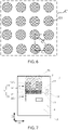
- the supporting columns 35 in the first depression 33 are uniformly arranged, and the supporting columns 35 in the second depression 34 are uniformly arranged.
- shapes of the plurality of supporting columns 35 include a cylindrical shape, a prismatic shape, a shape of a frustum of a cone, a shape of a frustum of a pyramid, or a special-shaped columnar shape.
- the plurality of supporting columns 35 are cylindrical.
- a radius L 1 of each supporting column 35 of the plurality of supporting columns 35 is in a range from 4 ⁇ m to 6 ⁇ m, e.g., 5 ⁇ m.
- a width L 2 of a gap 36 between two adjacent supporting columns 35 is in a range from 3 ⁇ m to 5 ⁇ m, e.g., 4 ⁇ m.
- a width L 3 of a gap 36 between two supporting columns 35 that are located on a diagonal line in four adjacent supporting columns 35 is in a range from 9 ⁇ m to 10 ⁇ m, e.g., 9.8 ⁇ m.
- the microfluidic channel backplane 1A provided in embodiments of the present disclosure further includes a bonding film layer 5 disposed on a side, away from the base 1, of the supporting layer 3.
- the bonding film layer 5 is configured such that the microfluidic channel backplane 1A is bonded to the cover plate 2A.
- the microfluidic channel backplane 1A is bonded to the cover plate 2A by bonding molecules in the bonding film layer 5 to molecules in the cover plate 2A.
- a material of the bonding film layer 5 and a material of the cover plate 2A are doped with the same metal substance, e.g., an iron-silicon alloy or a copper-silicon alloy.
- a chemical bond is formed in the iron-silicon alloy or the copper-silicon alloy to bond and encapsulate the microfluidic channel backplane 1A and the cover plate 2A.
- the film structure of the microfluidic channel backplane 1A further includes an electrode layer 6 disposed at a side of the plurality of microfluidic channels 21 proximate to or away from the base 1.
- embodiments of the present disclosure further provide a cover plate 2A of a microfluidic detection chip, and the cover plate 2A is provided with two sample-adding openings 71 and a detection channel 72 therein.
- the two sample-adding openings 71 are used for communicating with the two second sample-adding sub-channels 312 of the microfluidic channel backplane 1A, respectively.
- the detection channel 72 is used for communicating with an end, away from the first enrichment sub-channel 321, of the second enrichment sub-channel 322 of the enrichment channel 32 in the microfluidic channel backplane 1A.
- a detection reagent 74 for detecting the sample to be detected is added into the detection channel 72.
- embodiments of the present disclosure further provide a microfluidic detection chip 3A, including the microfluidic channel backplane 1A as described in any of the above embodiments, and the cover plate 2A arranged opposite to the microfluidic channel backplane 1A.
- the cover plate 2A is provided with two sample-adding openings 71 therein, and the two sample-adding openings 71 are communicated with the two second sample-adding sub-channels 312, respectively.
- the cover plate 2A includes the detection channel 72 arranged in a U shape. As shown in FIG. 17 , the detection channel 72 is communicated with an end, away from the first enrichment sub-channel 321, of the second enrichment sub-channel 322 of the enrichment channel 32 in the microfluidic channel backplane 1A.
- the cover plate 2A is provided with two detection openings 73 therein, and the two detection openings 73 are respectively disposed at two ends of the detection channel 72 and are communicated with the detection channel 72.
- the two detection openings 73 are configured to be coupled with an external detection device (the external detection device is not shown in FIG. 17 ), so as to apply a second driving signal to microfluid flowing through the detection channel, and are configured to cooperate with the driving electrode 62 to which the first driving signal is applied in the microfluidic channel backplane to form an electrical field for driving movement of the microfluid.
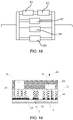
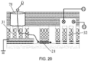
- droplets Q of the sample to be detected are added into the sample-adding channel 31 through the sample-adding opening 71, and a specific principle that the sample molecules to be detected flowing through the plurality of microfluidic channels 21 from the sample-adding channel 31 to the enrichment channel 32 are enriched is as follows: as shown in FIG.
- the droplets of the sample to be detected are added into the sample-adding channel 31 through the sample-adding opening 71; a driving signal is applied to the driving electrode 62, and the driving electrode 62 transmits the first driving signal; and the two detection openings 72 are respectively coupled to a first signal terminal V1 and a second signal terminal V2 of the external detection device, so as to apply the second driving signal to the microfluid flowing through the detection channel 72. Therefore, the two detection openings 72 cooperate with the driving electrode 62 to form the electrical field for driving the movement of the microfluid.
- the sample molecules to be detected flow through the plurality of microfluidic channels 21 from the sample-adding channel 31 to the enrichment channel 32, during which the sample molecules to be detected are enriched. As shown in FIGS. 17 and 18 , the detection unit 8 detects the sample molecules to be detected in the enrichment channel 32.
- the detection unit 8 may include a detection module 81 that detects different substances in the sample to be detected, e.g., a detection module 81 that detects specific detection antibodies.
- the detection unit 8 may include a detection module 82 that sequentially detects the substances in the sample to be detected.
- the detection unit 8 may include an optical detection module 83 that performs an optical detection on the substances in the sample to be detected.
- the detection unit 8 may include an electrical detection module 84 that performs an electrical detection on the substances in the sample to be detected.
- the detection unit 8 may include a detection module 85 including filtering and sifting functions.
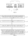
- embodiments of the present disclosure further provide a method of manufacturing a microfluidic channel backplane, and the method includes S1 to S4.
- a base 1 is provided, and a microfluidic channel film 02 is formed on a side of the base 1.
- the microfluidic channel film 02 is formed with a plurality of microfluidic channels 21 therein.
- Each microfluidic channel 21 of the plurality of microfluidic channels 21 includes a first end 211 and a second end 212.
- a supporting film 03 is formed on a side of the microfluidic channel film 02 away from the base 1.
- S3 as shown in (c) of FIG.
- the supporting film 03 is patterned to form a first depression 33, a second depression 34, and a plurality of supporting columns 35 located in the first depression 33 and the second depression 34.
- the first depression 33 and gaps 36 between supporting columns 35 located in the first depression 33 form a sample-adding channel 31.
- the second depression 34 and gaps 36 between supporting columns 35 located in the second depression 34 form an enrichment channel 32, and the enrichment channel 32 includes a first enrichment sub-channel 321 and a second enrichment sub-channel 322 that are communicated with each other.
- the microfluidic channel film 02 is etched downwards to form a first communication opening 211a at a position corresponding to first ends 211 of the plurality of microfluidic channels 21, so that the first ends 211 of the plurality of microfluidic channels 21 are communicated with the sample-adding channel 31, and to form a second communication opening 212a at a position corresponding to second ends 212 of the plurality of microfluidic channels 21, so that the second ends 212 of the plurality of microfluidic channels 21 are communicated with the first enrichment sub-channel 321 of the enrichment channel 32.
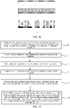
- the method of manufacturing the microfluidic channel backplane further includes S11 and S12.
- a conductive film 06 is formed on a side of the microfluidic channel film 02 away from the base 1.
- the conductive film 06 is patterned to form a control electrode 61 and a driving electrode 62.
- An orthogonal projection of the control electrode 61 on the base 1 is at least partially overlapped with an orthogonal projection of each microfluidic channel 21 of the plurality of microfluidic channels 21 on the base 1.
- An orthogonal projection of the driving electrode 62 on the base 1 is at least partially overlapped with an orthogonal projection of the sample-adding channel 31 on the base 1. As shown in FIG.
- the microfluidic channel film that is formed with the plurality of microfluidic channels 21 therein is formed on the side of the base in S1, and the method of manufacturing the microfluidic channel backplane provided in embodiments of the present disclosure further includes S01 and S02.
- a foundation layer 4 including a plurality of grooves is formed on a side of the base 1.
- a nanoimprint process is taken as an example, and a material of a foundation film layer with a specific thickness is formed on the base 1 by directly using a film forming process to obtain the foundation film layer.
- the material of the foundation film layer may be an inorganic material, such as silicon dioxide or silicon nitride, or a metal material, such as aluminum (Al) or molybdenum (Mo), or an organic material, such as photoresist (PR).
- the thickness of the foundation film layer may be approximately equal to 100 ⁇ m.
- Imprint adhesive is coated on the foundation film layer, then the imprint adhesive is imprinted by using an imprint template and cured, and a patterned imprint adhesive is obtained by demoulding.
- the foundation film layer that is not covered by the imprint adhesive is etched.
- the foundation film layer that is not covered by the imprint adhesive is etched away by using a dry etching process, as shown in (B) and (b) of FIG. 4 , so as to form the plurality of grooves 41 to obtain the foundation layer 4.
- a material of the microfluidic channel film 02 is deposited on a side of the foundation layer 4 away from the base 1.
- a microfluidic channel 21 is integrally formed over each groove 41 of the plurality of grooves 41.
- the material of the microfluidic channel layer is naturally deposited and grown through the deposition process on the foundation layer 4 formed with the plurality of grooves 41 therein. As shown in (c1) and (c2) of FIG. 4 , the material of the microfluidic channel layer gradually adheres to the foundation layer 4 during the deposition process to form the plurality of microfluidic channels 21 over the plurality of grooves 41.
- the deposition process may be a physical vapor deposition (PVD) process, such as a sputtering process; the deposition process may also be a chemical vapor deposition (CVD) process, such as a plasma enhanced chemical vapor deposition (PECVD) process, an atomic layer deposition (ALD) process, etc.
- PVD physical vapor deposition
- CVD chemical vapor deposition
- PECVD plasma enhanced chemical vapor deposition
- ALD atomic layer deposition
- a template with a convex structure of a detection channel is manufactured.
- a cover plate material is poured on the template, and then is removed to form a cover plate with a detection channel.
- biochemical detection reagent is added into the detection channel.
- microfluidic channel backplane 1A and the cover plate 2A are bonded to form the microfluidic detection chip 3A.
Landscapes
- Chemical & Material Sciences (AREA)
- Health & Medical Sciences (AREA)
- Dispersion Chemistry (AREA)
- Analytical Chemistry (AREA)
- General Health & Medical Sciences (AREA)
- Clinical Laboratory Science (AREA)
- Hematology (AREA)
- Chemical Kinetics & Catalysis (AREA)
- Physics & Mathematics (AREA)
- Life Sciences & Earth Sciences (AREA)
- Biochemistry (AREA)
- General Physics & Mathematics (AREA)
- Immunology (AREA)
- Pathology (AREA)
- Physical Or Chemical Processes And Apparatus (AREA)
Applications Claiming Priority (1)
| Application Number | Priority Date | Filing Date | Title |
|---|---|---|---|
| PCT/CN2020/073972 WO2021147072A1 (fr) | 2020-01-23 | 2020-01-23 | Plaque arrière de canal microfluidique et son procédé de fabrication, et puce de détection microfluidique |
Publications (2)
| Publication Number | Publication Date |
|---|---|
| EP4095512A1 true EP4095512A1 (fr) | 2022-11-30 |
| EP4095512A4 EP4095512A4 (fr) | 2023-01-18 |
Family
ID=76992766
Family Applications (1)
| Application Number | Title | Priority Date | Filing Date |
|---|---|---|---|
| EP20891412.7A Pending EP4095512A4 (fr) | 2020-01-23 | 2020-01-23 | Plaque arrière de canal microfluidique et son procédé de fabrication, et puce de détection microfluidique |
Country Status (4)
| Country | Link |
|---|---|
| US (2) | US12233410B2 (fr) |
| EP (1) | EP4095512A4 (fr) |
| CN (1) | CN113614509B (fr) |
| WO (1) | WO2021147072A1 (fr) |
Family Cites Families (17)
| Publication number | Priority date | Publication date | Assignee | Title |
|---|---|---|---|---|
| US6943034B1 (en) * | 1991-11-22 | 2005-09-13 | Affymetrix, Inc. | Combinatorial strategies for polymer synthesis |
| US20050063865A1 (en) * | 2002-09-27 | 2005-03-24 | Ulrich Bonne | Phased VII micro fluid analyzer having a modular structure |
| US20050034990A1 (en) * | 2003-08-12 | 2005-02-17 | Crooks Richard M. | System and method for electrokinetic trapping and concentration enrichment of analytes in a microfluidic channel |
| US20050277125A1 (en) * | 2003-10-27 | 2005-12-15 | Massachusetts Institute Of Technology | High-density reaction chambers and methods of use |
| JP2007163459A (ja) * | 2005-11-18 | 2007-06-28 | Sharp Corp | 分析用マイクロチップ |
| US20080070311A1 (en) * | 2006-09-19 | 2008-03-20 | Vanderbilt University | Microfluidic flow cytometer and applications of same |
| US8186913B2 (en) * | 2007-04-16 | 2012-05-29 | The General Hospital Corporation | Systems and methods for particle focusing in microchannels |
| WO2009004533A1 (fr) * | 2007-07-03 | 2009-01-08 | Nxp B.V. | Puce microfluidique et procédé pour manipuler des gouttelettes de fluide |
| WO2009052354A2 (fr) * | 2007-10-17 | 2009-04-23 | Advanced Liquid Logic, Inc. | Structures d'actionneur à gouttelettes |
| CN101670998B (zh) * | 2009-09-16 | 2011-10-26 | 哈尔滨工业大学 | 点面电极系统及利用该系统进行微流体驱动的方法 |
| EP2602608B1 (fr) * | 2011-12-07 | 2016-09-14 | Imec | Analyse et tri des cellules biologiques dans un écoulement |
| CN104251910B (zh) * | 2013-06-29 | 2017-04-05 | 黄辉 | 一种基于光学检测的微流控芯片及其制备方法 |
| CN104698064B (zh) * | 2015-03-18 | 2015-12-02 | 青岛大学 | 一种多通道微流控-固相萃取-质谱联用装置及制备方法 |
| WO2016154302A1 (fr) | 2015-03-23 | 2016-09-29 | The University Of North Carolina At Chapel Hill | Processeur moléculaire universel pour la médecine de précision |
| CN108226012B (zh) * | 2018-01-02 | 2021-01-26 | 京东方科技集团股份有限公司 | 微流控芯片、分析装置和微流控芯片的控制方法 |
| CN108956467B (zh) | 2018-08-09 | 2022-04-22 | 京东方科技集团股份有限公司 | 一种微流控芯片及其工作方法 |
| CN118604090A (zh) * | 2019-03-01 | 2024-09-06 | 南京岚煜生物科技有限公司 | 一种具有五层结构的多通道微流体凝血检测芯片 |
-
2020
- 2020-01-23 EP EP20891412.7A patent/EP4095512A4/fr active Pending
- 2020-01-23 CN CN202080000081.9A patent/CN113614509B/zh active Active
- 2020-01-23 WO PCT/CN2020/073972 patent/WO2021147072A1/fr not_active Ceased
- 2020-01-23 US US17/292,277 patent/US12233410B2/en active Active
-
2025
- 2025-01-17 US US19/027,491 patent/US20250170569A1/en active Pending
Also Published As
| Publication number | Publication date |
|---|---|
| CN113614509B (zh) | 2023-12-19 |
| CN113614509A (zh) | 2021-11-05 |
| US20250170569A1 (en) | 2025-05-29 |
| EP4095512A4 (fr) | 2023-01-18 |
| US20220048028A1 (en) | 2022-02-17 |
| WO2021147072A1 (fr) | 2021-07-29 |
| US12233410B2 (en) | 2025-02-25 |
Similar Documents
| Publication | Publication Date | Title |
|---|---|---|
| DE60018425T2 (de) | Elastomerische Mikropumpen- oder Mikroventilsysteme | |
| US7501279B2 (en) | Microwell arrays with nanoholes | |
| US10054536B2 (en) | Microfluidic particle analysis method, device and system | |
| DE60036420T2 (de) | Mikrofluidischer Artikel | |
| JP4931330B2 (ja) | マイクロ流体構造、特にバイオチップを製造する方法および該方法によって得られた構造 | |
| US20050023156A1 (en) | Nanostructured material transport devices and their fabrication by application of molecular coatings to nanoscale channels | |
| WO2003020946A2 (fr) | Fabrication de dispositifs moleculaires de petite echelle au moyen d'un assemblage fluidique | |
| WO2007101174A2 (fr) | Dispositifs et procedes magneto-fluidiques numeriques | |
| US20100003666A1 (en) | Microfluidic Methods for Diagnostics and Cellular Analysis | |
| KR20100087130A (ko) | 전기역학적 농축 장치 및 그의 사용 방법 | |
| Khandelwal et al. | Self-assembled microtubular electrodes for on-chip low-voltage electrophoretic manipulation of charged particles and macromolecules | |
| JP2017526915A (ja) | センシング装置 | |
| US7438851B2 (en) | Microsensor with a well having a membrane disposed therein | |
| US20250170569A1 (en) | Microfluidic channel backplane and microfluidic detection chip | |
| KR20230140740A (ko) | 3차원 전극 기반 미세유체 측정장치 및 그 제조방법 | |
| CN113333041A (zh) | 一种细胞捕获与检测微流控芯片 | |
| CN114225981A (zh) | 一种基于微液滴控制芯片的离子选择膜制备装置及方法 | |
| KR102186264B1 (ko) | 개방형 미세유체 채널 일체형 바이오센서 및 이의 제조 방법 | |
| US11944965B2 (en) | Microfluidic device | |
| CN117696133B (zh) | 用于外泌体处理的微流控芯片及其制作方法 | |
| CN119186660B (zh) | 微流控芯片、制造方法以及微液滴生成方法 | |
| KR20150117110A (ko) | 랩온어칩 및 이의 제조 방법 | |
| EP3222350A1 (fr) | Aiguilles creuses flexibles et cantilevers et leur procédé de fabrication | |
| CN110523447B (zh) | 一种对细胞多角度力学测量的微流控芯片及其制作方法 | |
| Folch et al. | Microwell arrays with nanoholes |
Legal Events
| Date | Code | Title | Description |
|---|---|---|---|
| STAA | Information on the status of an ep patent application or granted ep patent |
Free format text: STATUS: UNKNOWN |
|
| STAA | Information on the status of an ep patent application or granted ep patent |
Free format text: STATUS: THE INTERNATIONAL PUBLICATION HAS BEEN MADE |
|
| PUAI | Public reference made under article 153(3) epc to a published international application that has entered the european phase |
Free format text: ORIGINAL CODE: 0009012 |
|
| STAA | Information on the status of an ep patent application or granted ep patent |
Free format text: STATUS: REQUEST FOR EXAMINATION WAS MADE |
|
| 17P | Request for examination filed |
Effective date: 20210531 |
|
| AK | Designated contracting states |
Kind code of ref document: A1 Designated state(s): AL AT BE BG CH CY CZ DE DK EE ES FI FR GB GR HR HU IE IS IT LI LT LU LV MC MK MT NL NO PL PT RO RS SE SI SK SM TR |
|
| A4 | Supplementary search report drawn up and despatched |
Effective date: 20221219 |
|
| RIC1 | Information provided on ipc code assigned before grant |
Ipc: B01L 3/00 20060101ALI20221214BHEP Ipc: G01N 15/02 20060101AFI20221214BHEP |
|
| DAV | Request for validation of the european patent (deleted) | ||
| DAX | Request for extension of the european patent (deleted) | ||
| STAA | Information on the status of an ep patent application or granted ep patent |
Free format text: STATUS: EXAMINATION IS IN PROGRESS |
|
| 17Q | First examination report despatched |
Effective date: 20260309 |