EP4096085A1 - Stromumwandlungsvorrichtung - Google Patents
Stromumwandlungsvorrichtung Download PDFInfo
- Publication number
- EP4096085A1 EP4096085A1 EP22175788.3A EP22175788A EP4096085A1 EP 4096085 A1 EP4096085 A1 EP 4096085A1 EP 22175788 A EP22175788 A EP 22175788A EP 4096085 A1 EP4096085 A1 EP 4096085A1
- Authority
- EP
- European Patent Office
- Prior art keywords
- power
- primary
- power conversion
- conversion device
- side converter
- Prior art date
- Legal status (The legal status is an assumption and is not a legal conclusion. Google has not performed a legal analysis and makes no representation as to the accuracy of the status listed.)
- Withdrawn
Links
Images






Classifications
-
- H—ELECTRICITY
- H02—GENERATION; CONVERSION OR DISTRIBUTION OF ELECTRIC POWER
- H02M—APPARATUS FOR CONVERSION BETWEEN AC AND AC, BETWEEN AC AND DC, OR BETWEEN DC AND DC, AND FOR USE WITH MAINS OR SIMILAR POWER SUPPLY SYSTEMS; CONVERSION OF DC OR AC INPUT POWER INTO SURGE OUTPUT POWER; CONTROL OR REGULATION THEREOF
- H02M3/00—Conversion of DC power input into DC power output
- H02M3/22—Conversion of DC power input into DC power output with intermediate conversion into AC
- H02M3/24—Conversion of DC power input into DC power output with intermediate conversion into AC by static converters
- H02M3/28—Conversion of DC power input into DC power output with intermediate conversion into AC by static converters using discharge tubes with control electrode or semiconductor devices with control electrode to produce the intermediate AC
- H02M3/325—Conversion of DC power input into DC power output with intermediate conversion into AC by static converters using discharge tubes with control electrode or semiconductor devices with control electrode to produce the intermediate AC using devices of a triode or a transistor type requiring continuous application of a control signal
- H02M3/335—Conversion of DC power input into DC power output with intermediate conversion into AC by static converters using discharge tubes with control electrode or semiconductor devices with control electrode to produce the intermediate AC using devices of a triode or a transistor type requiring continuous application of a control signal using semiconductor devices only
- H02M3/33569—Conversion of DC power input into DC power output with intermediate conversion into AC by static converters using discharge tubes with control electrode or semiconductor devices with control electrode to produce the intermediate AC using devices of a triode or a transistor type requiring continuous application of a control signal using semiconductor devices only having several active switching elements
- H02M3/33576—Conversion of DC power input into DC power output with intermediate conversion into AC by static converters using discharge tubes with control electrode or semiconductor devices with control electrode to produce the intermediate AC using devices of a triode or a transistor type requiring continuous application of a control signal using semiconductor devices only having several active switching elements having at least one active switching element at the secondary side of an isolation transformer
- H02M3/33584—Bidirectional converters
-
- H—ELECTRICITY
- H02—GENERATION; CONVERSION OR DISTRIBUTION OF ELECTRIC POWER
- H02M—APPARATUS FOR CONVERSION BETWEEN AC AND AC, BETWEEN AC AND DC, OR BETWEEN DC AND DC, AND FOR USE WITH MAINS OR SIMILAR POWER SUPPLY SYSTEMS; CONVERSION OF DC OR AC INPUT POWER INTO SURGE OUTPUT POWER; CONTROL OR REGULATION THEREOF
- H02M1/00—Details of apparatus for conversion
- H02M1/08—Circuits specially adapted for the generation of control voltages for semiconductor devices incorporated in static converters
-
- H—ELECTRICITY
- H02—GENERATION; CONVERSION OR DISTRIBUTION OF ELECTRIC POWER
- H02M—APPARATUS FOR CONVERSION BETWEEN AC AND AC, BETWEEN AC AND DC, OR BETWEEN DC AND DC, AND FOR USE WITH MAINS OR SIMILAR POWER SUPPLY SYSTEMS; CONVERSION OF DC OR AC INPUT POWER INTO SURGE OUTPUT POWER; CONTROL OR REGULATION THEREOF
- H02M1/00—Details of apparatus for conversion
- H02M1/38—Means for preventing simultaneous conduction of switches
-
- H—ELECTRICITY
- H02—GENERATION; CONVERSION OR DISTRIBUTION OF ELECTRIC POWER
- H02M—APPARATUS FOR CONVERSION BETWEEN AC AND AC, BETWEEN AC AND DC, OR BETWEEN DC AND DC, AND FOR USE WITH MAINS OR SIMILAR POWER SUPPLY SYSTEMS; CONVERSION OF DC OR AC INPUT POWER INTO SURGE OUTPUT POWER; CONTROL OR REGULATION THEREOF
- H02M3/00—Conversion of DC power input into DC power output
- H02M3/22—Conversion of DC power input into DC power output with intermediate conversion into AC
- H02M3/24—Conversion of DC power input into DC power output with intermediate conversion into AC by static converters
- H02M3/28—Conversion of DC power input into DC power output with intermediate conversion into AC by static converters using discharge tubes with control electrode or semiconductor devices with control electrode to produce the intermediate AC
- H02M3/325—Conversion of DC power input into DC power output with intermediate conversion into AC by static converters using discharge tubes with control electrode or semiconductor devices with control electrode to produce the intermediate AC using devices of a triode or a transistor type requiring continuous application of a control signal
- H02M3/335—Conversion of DC power input into DC power output with intermediate conversion into AC by static converters using discharge tubes with control electrode or semiconductor devices with control electrode to produce the intermediate AC using devices of a triode or a transistor type requiring continuous application of a control signal using semiconductor devices only
- H02M3/33507—Conversion of DC power input into DC power output with intermediate conversion into AC by static converters using discharge tubes with control electrode or semiconductor devices with control electrode to produce the intermediate AC using devices of a triode or a transistor type requiring continuous application of a control signal using semiconductor devices only with automatic control of the output voltage or current, e.g. flyback converters
- H02M3/33515—Conversion of DC power input into DC power output with intermediate conversion into AC by static converters using discharge tubes with control electrode or semiconductor devices with control electrode to produce the intermediate AC using devices of a triode or a transistor type requiring continuous application of a control signal using semiconductor devices only with automatic control of the output voltage or current, e.g. flyback converters with digital control
-
- H—ELECTRICITY
- H02—GENERATION; CONVERSION OR DISTRIBUTION OF ELECTRIC POWER
- H02M—APPARATUS FOR CONVERSION BETWEEN AC AND AC, BETWEEN AC AND DC, OR BETWEEN DC AND DC, AND FOR USE WITH MAINS OR SIMILAR POWER SUPPLY SYSTEMS; CONVERSION OF DC OR AC INPUT POWER INTO SURGE OUTPUT POWER; CONTROL OR REGULATION THEREOF
- H02M1/00—Details of apparatus for conversion
- H02M1/0048—Circuits or arrangements for reducing losses
- H02M1/0054—Transistor switching losses
-
- H—ELECTRICITY
- H02—GENERATION; CONVERSION OR DISTRIBUTION OF ELECTRIC POWER
- H02M—APPARATUS FOR CONVERSION BETWEEN AC AND AC, BETWEEN AC AND DC, OR BETWEEN DC AND DC, AND FOR USE WITH MAINS OR SIMILAR POWER SUPPLY SYSTEMS; CONVERSION OF DC OR AC INPUT POWER INTO SURGE OUTPUT POWER; CONTROL OR REGULATION THEREOF
- H02M1/00—Details of apparatus for conversion
- H02M1/0048—Circuits or arrangements for reducing losses
- H02M1/0054—Transistor switching losses
- H02M1/0058—Transistor switching losses by employing soft switching techniques, i.e. commutation of transistors when applied voltage is zero or when current flow is zero
-
- H—ELECTRICITY
- H02—GENERATION; CONVERSION OR DISTRIBUTION OF ELECTRIC POWER
- H02M—APPARATUS FOR CONVERSION BETWEEN AC AND AC, BETWEEN AC AND DC, OR BETWEEN DC AND DC, AND FOR USE WITH MAINS OR SIMILAR POWER SUPPLY SYSTEMS; CONVERSION OF DC OR AC INPUT POWER INTO SURGE OUTPUT POWER; CONTROL OR REGULATION THEREOF
- H02M1/00—Details of apparatus for conversion
- H02M1/08—Circuits specially adapted for the generation of control voltages for semiconductor devices incorporated in static converters
- H02M1/083—Circuits specially adapted for the generation of control voltages for semiconductor devices incorporated in static converters for the ignition at the zero crossing of the voltage or the current
-
- H—ELECTRICITY
- H02—GENERATION; CONVERSION OR DISTRIBUTION OF ELECTRIC POWER
- H02M—APPARATUS FOR CONVERSION BETWEEN AC AND AC, BETWEEN AC AND DC, OR BETWEEN DC AND DC, AND FOR USE WITH MAINS OR SIMILAR POWER SUPPLY SYSTEMS; CONVERSION OF DC OR AC INPUT POWER INTO SURGE OUTPUT POWER; CONTROL OR REGULATION THEREOF
- H02M1/00—Details of apparatus for conversion
- H02M1/32—Means for protecting converters other than automatic disconnection
- H02M1/34—Snubber circuits
- H02M1/346—Passive non-dissipative snubbers
-
- Y—GENERAL TAGGING OF NEW TECHNOLOGICAL DEVELOPMENTS; GENERAL TAGGING OF CROSS-SECTIONAL TECHNOLOGIES SPANNING OVER SEVERAL SECTIONS OF THE IPC; TECHNICAL SUBJECTS COVERED BY FORMER USPC CROSS-REFERENCE ART COLLECTIONS [XRACs] AND DIGESTS
- Y02—TECHNOLOGIES OR APPLICATIONS FOR MITIGATION OR ADAPTATION AGAINST CLIMATE CHANGE
- Y02B—CLIMATE CHANGE MITIGATION TECHNOLOGIES RELATED TO BUILDINGS, e.g. HOUSING, HOUSE APPLIANCES OR RELATED END-USER APPLICATIONS
- Y02B70/00—Technologies for an efficient end-user side electric power management and consumption
- Y02B70/10—Technologies improving the efficiency by using switched-mode power supplies [SMPS], i.e. efficient power electronics conversion e.g. power factor correction or reduction of losses in power supplies or efficient standby modes
Definitions
- the present invention relates to a power conversion device for performing power conversion between DC power and other DC power by using semiconductor switching elements, and in particular, to a technology to reduce a power loss that occurs in each of the semiconductor switching elements.
- a single-phase full-bridge converter is configured using semiconductor switching elements.
- the single-phase full-bridge converter is a converter that converts DC power to AC power, or converts AC power to DC power. Then, using two converters each being the single-phase full-bridge converter, their respective AC terminals are connected to each other through a transformer, to thereby achieve a power conversion device which can perform DC/DC conversion and whose primary side and secondary side are insulated from each other.
- Such a power conversion device has also been referenced which can perform DC/DC conversion with a low loss in such a manner that a snubber capacitor is used for each of the semiconductor switching elements to thereby achieve soft switching, namely, zero-voltage switching which causes the semiconductor switching element to perform turn-on operation at zero voltage (see, for example, Non-Patent Document 2).
- Patent Document 1 US 5 027 264 A
- the power conversion device is referenced which is configured with the single-phase full bridges or the three-phase bridges and converts DC power to other DC power, and further, it is disclosed that so-called zero-voltage switching can be achieved.
- the zero-voltage switching can not be achieved in some cases depending on conditions, and thus there is a problem that the power conversion device is insufficient in surely achieving DC/DC conversion with a low loss.
- An object of the invention is to provide a power conversion device which can surely achieve zero-voltage switching, to thereby convert DC power to other DC power with a low loss.
- a power conversion device comprises:
- the capacitance of the snubber capacitor is set so that, at the time the primary-side converter executes a power-transferring operation, in that converter, a polarity of a current flowing through the AC terminals changes after completion of charging/discharging of the snubber capacitor due to changes in on/off states of the semiconductor elements;
- the control device controls the turning on/off, by setting a short-circuit prevention period Td for preventing short circuiting from occurring in each of the respective switching legs due to simultaneous turn-on operations of the positive-side and negative-side semiconductor switching elements commonly included therein, so as to achieve zero-voltage switching which causes each of these semiconductor switching elements to perform a turn-on operation at zero voltage.
- the short-circuit prevention period Td for the primary-side converter is set so as to prevent occurrence of short-circuiting of the snubber capacitor connected to the semiconductor switching element, due to the turn-on operation of that semiconductor switching element.
- the short-circuit prevention period Td for either one of the primary-side and secondary-side converters is set to have a relationship with a current-polarity reversal time Tcmtt so that Td ⁇ Tcmtt is satisfied, the current-polarity reversal time Tcmtt being a period of time, when that converter executes a power-transferring operation, from a start time of the short-circuit prevention period Td until a polarity of an AC current flowing through the inductance element is reversed.
- the short-circuit prevention time determines whether zero-voltage switching is achieved or not.
- the short-circuit prevention time is adequately set in the above manner.
- the power conversion device can surely achieve zero-voltage switching, to thereby convert DC power to other DC power with a low loss.
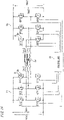
- FIG. 1 is a diagram showing an entire configuration of a power conversion device according to Embodiment 1 of the invention.
- This power conversion device includes: a main circuit which has two converters 1, 2 placed in a primary-side and a secondary-side and each configured as a single-phase full bridge, and one single-phase transformer TR; and a control device 10; and serves to convert DC power of a primary-side capacitor Cdcl to which a primary-side DC voltage Vdc1 is applied, to DC power of a secondary-side capacitor Cdc2 to which a secondary-side DC voltage Vdc2 is applied, through the transformer TR.
- FIG. 1 is just an example, and any product may fall within the applicable scope of this invention so far as it converts DC power to other DC power by using a bridge comprising semiconductor switching elements Q.
- the circuit in FIG. 1 allows power conversion in which electric power is transmitted and received between the primary side and the secondary side in an unrestricted manner, so that the direction of the power can be controlled without restrictions.
- a positive-side semiconductor switching element Q11 and a negative-side semiconductor switching element Q12 paired with freewheel diodes D11, D12 connected, respectively, in reverse parallel thereto, are serially connected to each other to form a switching leg S11. Both ends of the switching leg S11 are connected to the capacitor Cdcl. An intermediate connection point of the switching leg S11 is connected to one of AC terminals of a primary-side winding W1 in the transformer TR.
- semiconductor switching elements Q Q11-Q14, Q21-Q24
- freewheel diodes D D11-D14, D21-D24
- An inductance Ls in FIG. 1 given as the inductance element indicates a leakage inductance of the transformer TR, and Ls/2 is placed equivalently in the primary side and the secondary side. Note that it is not necessarily required to use only the leakage inductance of the transformer TR as the inductance Ls and an additional inductance may be connected thereto.
- a second switching leg S12 is formed, both ends of which is connected to the capacitor Cdcl, and an intermediate connection point of which is connected to the other one of the AC terminals of the primary-side winding W1 in the transformer TR.
- the primary-side converter 1 in FIG. 1 uses two switching legs S11, S12, so that it is generally called “single-phase full-bridge circuit", “H bridge circuit” or the like.
- a single-phase full-bridge circuit with two switching legs S21, S22 is formed, like in the primary side.
- a capacitor Cdc2 is connected, and to its AC side, AC terminals of a secondary-side winding W2 in the transformer TR are connected.
- the circuit in FIG. 1 is a circuit which converts a DC voltage to an AC voltage and thereafter, converts the AC voltage to a DC voltage while ensuring insulation by way of the transformer TR. Note that, when insulation is not required, only an inductance that is equivalent to Ls may be connected as the inductance element.
- each of the capacitors Cdcl, Cdc2 an electrolytic capacitor, a film capacitor or the like may be used; however, because a high-frequency current flows through the capacitor Cdcl or Cdc2, it is better to use a film capacitor. Using a film capacitor makes it possible to prolong the lifetime.
- a semiconductor switching element such as, an IGBT (Insulated-Gate Bipolar Transistor), a GCT (Gate Commutated Turn-off Thyristor), a MOSFET (Metal-Oxide-Semiconductor Field-Effect Transistor) or the like, is used.
- IGBT Insulated-Gate Bipolar Transistor
- GCT Gate Commutated Turn-off Thyristor
- MOSFET Metal-Oxide-Semiconductor Field-Effect Transistor
- the turn ratio of the transformer TR (a ratio of the number of turns of the primary-side winding W1 to the number of turns of the secondary-side winding W2) be matched to a ratio of the primary-side DC voltage Vdc1 to the secondary-side DC voltage Vdc2.
- the turn ratio of the transformer TR is determined as 1:3.
- the secondary-side DC voltage Vdc2 is assumed to be a voltage converted correspondingly from the primary-side voltage by using the turn ratio of the transformer TR.
- the control device 10 can control power P transmitted/received between the primary side and the secondary side, by sending driving signals to the semiconductor switching elements Q11, Q12, Q13, Q14 and Q21, Q22, Q23, Q24 to thereby control turning-on/off of them.
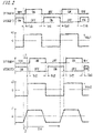
- FIG. 2 is a timing chart showing operations at respective portions under control of the control device 10, in which shown are respective on/off states of the semiconductor switching elements Q11, Q12, Q13, Q14 and Q21, Q22, Q23, Q24, and output voltages v1, v2 of the primary-side and secondary-side converters 1, 2, and further, a primary-side output current i1.
- the semiconductor switching elements Q11 and Q14 operate in mutually the same switching state, and the semiconductor switching elements Q12 and Q13 operate in mutually the same switching state.
- the semiconductor switching elements Q11, Q14 are not turned on simultaneously with the semiconductor switching elements Q12, Q13; these switching elements are each turned on and turned off, ideally, in respective 180 degrees per one cycle (360 degrees), and the semiconductor switching elements Q11, Q14 and the semiconductor switching elements Q12, Q13 perform mutually inverted operations.
- a short-circuit prevention period (referred to, also as dead time, in this application) Td1 is inserted.
- the dead time means a period where the semiconductor switching elements Q11, Q12 are both turned off (or Q13, Q14 are both turned off).
- the semiconductor switching elements Q21 and Q24 operate in mutually the same switching state, and the semiconductor switching elements Q22 and Q23 operate in mutually the same switching state.
- a dead time Td2 where the semiconductor switching elements Q21, Q22 are both turned off (or Q23, Q24 are both turned off) is inserted.
- Switching in the primary-side converter 1 and the secondary-side converter 2 is executed in their phases shifted by a phase difference ⁇ [rad] therebetween.
- the output current i1 of the primary-side converter 1 changes to provide a current waveform as shown in FIG. 2 .
- controlling the output current i1 by using the phase difference ⁇ makes it possible to control the power P.
- ⁇ denotes a value resulting from multiplying a switching frequency fs by 2 ⁇ .
- ZVS zero-voltage switching
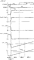
- FIG. 3 is a timing chart showing switching operations in the primary-side converter 1 (as described later, herein serving as a power-transferring side converter), in which, attention is paid on an event where the switching states in the primary-side converter 1 change, and there are specifically shown: switching states of the semiconductor switching elements Q11, Q12, Q13, Q14; the output voltage v1; voltages Vce12, Vce13 across the respective semiconductor switching elements Q12, Q13; currents ic12, ic13 flowing through the semiconductor switching elements Q12, Q13 or the freewheel diodes D12, D13, respectively (when positive, currents flowing through the semiconductor switching elements; when negative, currents flowing through the freewheel diodes); voltages Vce11, Vce14 across the respective semiconductor switching elements Q11, Q14; currents ic11, ic14 flowing through the semiconductor switching elements Q11, Q14 or the freewheel diodes D11, D14, respectively (when positive, currents flowing through the semiconductor switching elements; when negative, currents flowing through the freewheel diodes);
- FIG. 2 a state where the power is transmitted from the primary side toward the secondary side is shown. Accordingly, in FIG. 3 , illustration is made focusing attention on the switching operations in the power-transferring side converter 1.
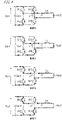
- FIG. 3 can be described in a manner divided to MODEO to MODE4, together with FIG. 4 in which current flowing states are shown.
- the leakage inductance is totally indicated by Ls, and the output voltage of the secondary-side converter 2 is simulated to be Vdc2.
- the semiconductor switching elements Q11, Q14 are in turned-off states, and the semiconductor switching elements Q12, Q13 are in turned-on states.
- the semiconductor switching elements Q12, Q13 change from "turned-on” to "turned-off” while the semiconductor switching elements Q11, Q14 are kept turned-off without change. Accordingly, the voltages Vce12, Vce13 across the semiconductor switching elements Q12, Q13 increase from zero to Vdcl, while the voltages Vce11, Vce14 across the semiconductor switching elements Q11, Q14 decrease from Vdc1 to zero. Further, the currents ic12, ic13 decrease from values in current-flowing states to zero, while the currents ic11, ic14 increase from zero to reach the currents equivalent to the output current i1. On this occasion, the currents are commutated from the semiconductor switching elements Q12, Q13 to the freewheel diodes D11, D14, thus causing turn-off losses in the semiconductor switching elements Q12, Q13.
- MODE1 is omitted from illustration in FIG. 4 , because the current-flows in that mode vary largely in a extremely short time and is thus difficult to be illustrated, even though the occurrence of the current commutation can not be avoided in Embodiment 1.
- the semiconductor switching elements Q11, Q14 change from “turned-off” to "turned-on”.
- the semiconductor switching elements Q12, Q13 are kept turned-off.
- the polarity of the output current i1 is negative, currents are already flowing through the freewheel diodes D11, D14.
- the respective voltages Vce11, Vce14 across them do not change, causing no turn-on loss.
- This phenomenon is called zero-voltage switching (ZVS), by which a switching loss can be reduced.
- the output current i1 changes from negative to positive.
- the currents having been flowing through the freewheel diodes D11, D14 flow instead through the semiconductor switching elements Q11, Q14.
- the length of the dead time Td1 for the power-transferring side converter 1 is set as follows. Namely, in FIG. 3 , the illustration has been made assuming that, relative to the dead time Td1, a current-polarity reversal time Tcmtt is longer that is a period of time from a start time of the dead time Td1 until the polarity of the output current i1 (an AC current flowing through the inductance Ls) is reversed.
- Embodiment 1 has a feature in that the dead time Td1 for the power-transferring side converter 1 is set equal to or less than the current-polarity reversal time Tcmtt until the polarity of the output current i1 is reversed.
- the dead time Td1 for the power-transferring side converter 1 is set so that a following Formula (3) is satisfied.
- the dead time Td1 when the dead time Td1 is set in a condition where the transferring power P is the rated power of the power conversion device, because a facility capacity is determined according to an operating condition where such largest power is handled, it is possible, as a result of reduction in the losses in that operating condition, to reduce a required capacity of a cooler, for example, to thereby achieve downsizing thereof.
- the dead time when the dead time is set according to an average value of the transferring power P under actual operations, the losses can be reduced in operating states over a long period of time, and this will result in improvement in the efficiency of the power-transferring.
- the power conversion device is used for offshore wind power generation or the like, an output of about 40 % of the rated value is promising in average.
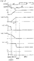
- FIG. 6 is a timing chart showing switching operations in the power-receiving side (secondary-side) converter 2, in which, attention is paid on an event where the switching states in the secondary-side converter 2 change, and there are specifically shown: switching states of the semiconductor switching elements Q21, Q22, Q23, Q24; the output voltage v2; voltages Vce22, Vce23 across the respective semiconductor switching elements Q22, Q23; currents ic22, ic23 flowing through the semiconductor switching elements Q22, Q23 or the freewheel diodes D22, D23, respectively (when positive, currents flowing through the semiconductor switching elements; when negative, currents flowing through the freewheel diodes); voltages Vce21, Vce24 across the respective semiconductor switching elements Q21, Q24; currents ic21, ic24 flowing through the semiconductor switching elements Q21, Q24 or the freewheel diodes D21, D24, respectively (when positive, currents flowing through the semiconductor switching elements; when negative, currents flowing through the freewheel diodes); and the output current i2 of
- FIG. 6 The phenomena shown in FIG. 6 can be described in a manner divided to MODEO to MODE3, together with FIG. 7 in which current flowing states are shown. Note that in FIG. 7 , the leakage inductance is totally indicated by Ls, and the output voltage of the primary-side converter 1 is simulated to be Vdc1.
- the semiconductor switching elements Q21, Q24 are in turned-off states, and the semiconductor switching elements Q22, Q23 are in turned-on states.
- the semiconductor switching elements Q22, Q23 change from "turned-on” to "turned-off” while the semiconductor switching elements Q21, Q24 are kept turned-off without change. Accordingly, the voltages Vce22, Vce23 across the semiconductor switching elements Q22, Q23 increase from zero to Vdc2, while the voltages Vce21, Vce24 across the semiconductor switching elements Q21, Q24 decrease from Vdc2 to zero. Further, the currents ic22, ic23 decrease from values in current-flowing states to zero, while the currents ic21, ic24 increase from zero to reach the currents equivalent to the output current i2. On this occasion, the currents are commutated from the semiconductor switching elements Q22, Q23 to the freewheel diodes D21, D24, thus causing turn-off losses in the semiconductor switching elements Q22, Q23.
- MODE1 is omitted from illustration in FIG. 7 for the same reason previously described about FIG. 4 for the aforementioned power-transferring side converter 1.
- the semiconductor switching elements Q21, Q24 change from “turned-off” to "turned-on”.
- the semiconductor switching elements Q22, Q23 are kept turned-off.
- the polarity of the output current i2 is negative, currents are already flowing through the freewheel diodes D21, D24.
- the semiconductor switching elements Q21, Q24 change from "turned-off” to "turned-on"
- the voltages Vce21, Vce24 across them do not change, causing no turn-on loss. Namely, a switching loss can be reduced by zero-voltage switching (ZVS).
- ZVS zero-voltage switching
- the dead time Td1 is required to be set short so as to satisfy the aforementioned Formula (3), whereas the dead time Td2 for the power-receiving side converter 2 may be set longer because, for that dead time, there is no restriction related to zero-voltage switching.
- the reliability of the semiconductor switching element generally tends to be lowered when the dead time is set short, when the dead time Td2 for the power-receiving side converter 2 is set longer than the short-set dead time Td1 for the power-transferring side converter 1, for example, the reliability of the device is improved because there is no dead time that is set unnecessarily short.
- the power conversion device serves to transmit the power always from the primary side to the secondary side
- a control method is conceivable in which either one of the primary-side and secondary-side converters 1, 2 which is under power-transferring operation is regarded as the power-transferring side converter 1(2) while the other one at that time is regarded as the power-receiving side converter 2(1), and then the dead times suited to the respective converters are set.
- this method at every time the direction of power flow changes, it is necessary to change the dead times for both converters 1, 2, thus causing complexity in control accordingly; however, there is an advantage in that zero-voltage switching is achieved in both converters 1, 2 regardless of the direction of power flow , so that a low-loss and highly-efficient operating characteristic is obtained.
- the rated voltage of the secondary-side semiconductor element (the switching element and the diode) is set higher than the rated voltage of the primary-side semiconductor element in such a manner that, in the transformer TR in FIG. 1 , the number of turns of the secondary-side winding W2 is made larger than the number of turns of the primary-side winding W1, to thereby establish a configuration which can perform boosting operation from a lower voltage to a higher voltage.
- Such a way for use is best suited to an DC/DC conversion application for performing boosting from a source of low-voltage energy, for example, renewable energy, etc. toward a high-voltage power system or load.
- semiconductor elements described in claim 1 of this application, that the semiconductor elements in the primary-side/power-transferring side converter 1 are each configured with the semiconductor switching element and the freewheel diode, while the semiconductor elements in the secondary-side/power-receiving side converter 2 are each configured with the diode only, without including the semiconductor switching element.
- the dead time Td1 for the converter 1 serving as the power-transferring side converter is set equal to or less than the current-polarity reversal time Tcmtt.
- the dead time for the power-transferring side converter 1 is set to be short and the dead time for the power-receiving side converter 2 is set to be long, it is possible to achieve zero-voltage switching to thereby provide a low-loss power conversion device, without affecting the reliability of the semiconductor element.
- FIG. 8 is a diagram showing an entire configuration of a power conversion device according to Embodiment 2 of the invention.
- the power conversion device includes: a main circuit which has two converters 1a, 2a placed in a primary-side and a secondary-side and each configured as a single-phase full bridge, and one single-phase transformer TR; and a control device 10.
- snubber capacitors Cs11, Cs12, Cs13, Cs14, Cs21, Cs22, Cs23, Cs24 are connected, respectively, in parallel to the semiconductor switching elements Q11, Q12, Q13, Q14, Q21, Q22, Q23, Q24 and the freewheel diodes D11, D12, D13, D14, D21, D22, D23, D24 that have been described using FIG. 1 .
- connection of the snubber capacitor makes it possible to moderate the change in voltage at the time of turning-off, to thereby create an effect of reducing the turn-off loss and noise.
- FIG. 9 is a timing chart showing switching operations in the primary-side (herein provided as the power-transferring side) converter 1a, in which, attention is paid on an event where the switching states in the primary-side converter 1a change, and there are specifically shown: switching states of the semiconductor switching elements Q11, Q12, Q13, Q14; the output voltage v1; voltages Vce12, Vce13 across the respective semiconductor switching elements Q12, Q13; currents ic12, ic13 flowing through the semiconductor switching elements Q12, Q13 or the freewheel diodes D12, D13, respectively (when positive, currents flowing through the semiconductor switching elements; when negative, currents flowing through the freewheel diodes); voltages Vce11, Vce14 across the respective semiconductor switching elements Q11, Q14; currents ic11, ic14 flowing through the semiconductor switching elements Q11, Q14 or the freewheel diodes D11, D14, respectively (when positive, currents flowing through the semiconductor switching elements; when negative, currents flowing through the freewheel diodes); and the output current
- FIG. 9 can be described in a manner divided to MODEO to MODE4, together with FIG. 10 and FIG. 11 in which current flowing states are shown. Note that in FIG. 10 and FIG. 11 , the leakage inductance is totally indicated by Ls, and the output voltage of the secondary-side converter 2a is simulated to be Vdc2.
- the semiconductor switching elements Q11, Q14 are in turned-off states, and the semiconductor switching elements Q12, Q13 are in turned-on states.
- the turn-off loss is derived from multiplication of a voltage by a current at the time of such change, in comparison to the case where no snubber capacitor is connected, it is possible to reduce the turn-off loss because the current is shut off in a state with a lower voltage.
- the snubber capacitors Cs12, Cs13 continue to be charged, and at the same time, the snubber capacitors Cs11, Cs14 continue to be discharged.
- the voltages Vce12, Vce13 reach Vdcl, and the voltage Vce11, Vce14 become nearly zero.
- the snubber capacitors Cs11, Cs12, Cs13, Cs14 are those having capacitances that allow charging of the snubber capacitors Cs12, Cs13 and discharging of the snubber capacitors Cs11, Cs14 to be completed at a time before the time at which switching occurs from MODE3 to MODE4 that are to be described later, namely, before the time at which the output current i1 changes from negative to positive.
- the semiconductor switching elements Q11, Q14 change from “turned-off” to "turned-on”.
- the semiconductor switching elements Q12, Q13 are kept turned-off. At this time, because the polarity of the output current i1 is negative, currents are already flowing through the freewheel diodes D11, D14.
- the dead time Td1 is set as described by the Formula (3) in Embodiment 1, namely, it is set equal to or less than the current-polarity reversal time Tcmtt.
- the output current i1 changes from negative to positive.
- the currents having been flowing through the freewheel diodes D11, D14 flow instead through the semiconductor switching elements Q11, Q14.
- Embodiment 1 a large difference from Embodiment 1 resides in MODE1A and MODE1B. Namely, when the snubber capacitors Cs11, Cs12, Cs13, Cs14 are connected, the snubber capacitors Cs12, Cs13 connected in parallel to the turned-off semiconductor switching elements Q12, Q13, are charged by taking a time Tc1, while the snubber capacitors Cs11, Cs14 connected in parallel to the semiconductor switching elements Q11, Q14 in the opposite side (in the side where turning-on is now going to be done) are discharged by taking the time Tc1.
- Embodiment 2 has a feature in that, in order to prevent occurrence of short-circuiting of the snubber capacitor connected to the semiconductor switching element, due to the turn-on operation of that semiconductor switching element, the length of the dead time Td1 is set as follows. Namely, in FIG. 9 , illustration has been made assuming that the dead time Td1 is longer than the charging/discharging time Tc1 of the snubber capacitor.
- Embodiment 2 has a feature in that the dead time Td1 for the power-transferring side converter 1a is set equal to or more than the charging/ discharging time Tc1 of the snubber capacitor, as represented by a following Formula (4). [ Mathematical 4 ] Td 1 ⁇ Tc 1
- the capacitances of the snubber capacitors Cs11, Cs12, Cs13, Cs14 are set so that charging of the snubber capacitors Cs12, Cs13 and discharging of the snubber capacitors Cs11, Cs14 are completed at a time before the time at which the output current i1 changes from negative to positive.
- FIG. 13 is a timing chart showing switching operations in the power-receiving side (secondary-side) converter 2a, in which, attention is paid on an event where the switching states in the secondary-side converter 2a change, and there are specifically shown: switching states of the semiconductor switching elements Q21, Q22, Q23, Q24; the output voltage v2; voltages Vce22, Vce23 across the respective semiconductor switching elements Q22, Q23; currents ic22, ic23 flowing through the semiconductor switching elements Q22, Q23 or the freewheel diodes D22, D23, respectively (when positive, currents flowing through the semiconductor switching elements; when negative, currents flowing through the freewheel diodes); voltages Vce21, Vce24 across the respective semiconductor switching elements Q21, Q24; currents ic21, ic24 flowing through the semiconductor switching elements Q21, Q24 or the freewheel diodes D21
- FIG. 13 can be described in a manner divided to MODEO to MODE3, together with FIG. 14 in which current flowing states are shown.
- the leakage inductance is totally indicated by Ls, and the output voltage of the primary-side converter 1a is simulated to be Vdc1.
- the semiconductor switching elements Q21, Q24 are in turned-off states, and the semiconductor switching elements Q22, Q23 are in turned-on states.
- the turn-off loss is derived from multiplication of a voltage by a current at the time of such change, in comparison to the case where no snubber capacitor is connected, it is possible to reduce the turn-off loss because the current is shut off in a state with a lower voltage.
- the semiconductor switching elements Q21, Q24 change from “turned-off” to "turned-on”.
- the semiconductor switching elements Q22, Q23 are kept turned-off. At this time, because the polarity of the output current i2 is negative, currents are already flowing through the freewheel diodes D21, D24.
- a large difference from Embodiment 1 resides in MODE1A, MODE1B as described for the aforementioned power-transferring side converter 1a. Namely, when the snubber capacitors Cs21, Cs22, Cs23, Cs24 are connected, the snubber capacitors Cs22, Cs23 connected in parallel to the turned-off semiconductor switching elements Q22, Q23, are charged by taking a time Tc2, while the snubber capacitors Cs21, Cs24 connected in parallel to the semiconductor switching elements Q21, Q24 in the opposite side (in the side where turning-on is now going to be done) are discharged by taking the time Tc2.
- the length of the dead time Td2 is set as follows. Namely, in FIG. 13 , illustration has been made assuming that the dead time Td2 is longer than the charging/discharging time Tc2 of the snubber capacitor.
- Embodiment 2 has a feature in that the dead time Td2 for the power-receiving side converter 2a is set equal to or more than the charging/ discharging time Tc2 of the snubber capacitor, as represented by a following Formula (5). [ Mathematical 5 ] Td 2 ⁇ Tc 2
- the dead time Td2 for the power-transferring side converter 1a is to be set based on the Formula (5), as described similarly with respect to the aforementioned Formula (4), because the charging/ discharging time Tc2 of the snubber capacitor varies according to the transferring power P, it is possible to reduce a required capacity of the cooler, for example, to thereby achieve downsizing thereof, when the dead time Td2 is, for example, set in a condition where the transferring power P is the rated power of the power conversion device.
- the dead times Td1 and Td2 for the primary-side (power-transferring side) and secondary-side (power-receiving side) converters 1a, 2a are set equal to or more than the charging/discharging times Tc1, Tc2 of the snubber capacitors, respectively.
- FIG. 16 is a diagram showing an entire configuration of a power conversion device according to Embodiment 3 of the invention.
- Embodiment 3 as shown in FIG. 16 , as for converters 1b, 2b, a three-phase bridge circuit configuration is employed.
- FIG. 1 and FIG. 8 two switching legs each comprising serially connected semiconductor switching elements are used and the converters 1(1a), 2(2a) are configured with single-phase full-bridge circuits, whereas, in Embodiment 3, three switching legs are used and the converters 1b, 2b are configured with three-phase bridge circuits.
- a three-phase transformer TR is used.
- the three-phase transformer TR may not necessarily be a transformer for three phases, and three single-phase transformers may be used as the three-phase transformer.
- the leakage inductance is indicated by Ls like in Embodiment 1, an additional inductance may be used. Note that when insulation is not required, only an inductance that is equivalent to Ls may be connected.
- the ripple currents flowing through the capacitors Cdcl, Cdc2 can be reduced.
- it is allowable to reduce the capacities of the capacitors, so that the power conversion device can be downsized.
- this invention is also effective because there is a problem related to zero-voltage switching, similar to that described in Embodiments 1, 2. That is, like in Embodiment 1, the dead time Td1 for the power-transferring side converter 1b is set equal to or less than the current-polarity reversal time Tcmtt.
- the dead time Td2 for the power-receiving side converter 2b may be set longer because, for that dead time, there is no restriction related to zero-voltage switching. Namely, when the dead time Td2 for the power-receiving side converter 2b is set longer than the dead time Td1 for the power-transferring side converter 1b, the reliability of the device is improved because there is no dead time that is set unnecessarily short.
- the rated voltage of the secondary-side semiconductor element is set higher than the rated voltage of the primary-side semiconductor element, to thereby establish a configuration which can perform boosting operation from a lower voltage to a higher voltage.
- Such a way for use is best suited to an DC/DC conversion application for performing boosting from a source of low-voltage energy, for example, renewable energy, etc. toward a high-voltage power system or load.
- the capacitances of the snubber capacitors are set so that charging/discharging of the snubber capacitors Cs are completed at a time before the time at which each current in the respective phases change from negative to positive.
- the dead times Td1 and Td2 for the converters 1b, 2b are set equal to or more than the charging/discharging times Tc1, Tc2 of the snubber capacitors of the converters 1b, 2b, respectively, it is possible to surely prevent occurrence of short-circuiting of the snubber capacitor connected to the semiconductor switching element, due to the turn-on operation of that semiconductor switching element.
- the charging/ discharging times Tc1, Tc2 of the snubber capacitors vary according to the transferring power P, it is possible to reduce a required capacity of the cooler, for example, to thereby achieve downsizing thereof, when the dead times Td1, Td2 are, for example, set in a condition where the transferring power P is the rated power of the power conversion device.
- FIG. 17 is a diagram showing a main circuit configuration of a power conversion device according to Embodiment 4 of the invention.
- the main circuit of the power conversion device of any one of Embodiments 1 to 3 is a unit cell 3
- plural unit cells for example, fifty unit cells, each being the unit cell 3, and their respective capacitors Cdcl (or Cdc2) to which the primary-side (or secondary-side) DC voltages are applied, are connected serially or in parallel to each other.
- the plural unit cells 3 are connected serially and in parallel to each other to thereby configure a main circuit, and the configuration shown in Embodiments 1 to 3 is applied to each of the unit cells 3, so that an effect similar to in Embodiments 1 to 3 is obtained for every unit cell 3.
- the operation test of the power conversion device can be simplified, and further the fabrication thereof becomes easier.
- silicon is generally used as materials of the semiconductor switching element and the freewheel diode; however, when a wide bandgap material, such as silicon carbide, a gallium nitride-based material, diamond or the like whose bandgap is wider than that of silicon, is used instead, it is possible to make the withstanding voltage of the semiconductor element higher, so that a higher voltage can be converted. Furthermore, it is possible to make switching faster, so that the transformer TR can be downsized.
- a wide bandgap material such as silicon carbide, a gallium nitride-based material, diamond or the like whose bandgap is wider than that of silicon
- the present invention covers the following aspects:
Landscapes
- Engineering & Computer Science (AREA)
- Power Engineering (AREA)
- Dc-Dc Converters (AREA)
- Inverter Devices (AREA)
Applications Claiming Priority (3)
| Application Number | Priority Date | Filing Date | Title |
|---|---|---|---|
| JP2015060607 | 2015-03-24 | ||
| PCT/JP2016/055501 WO2016152366A1 (ja) | 2015-03-24 | 2016-02-24 | 電力変換装置 |
| EP16768269.9A EP3276809A4 (de) | 2015-03-24 | 2016-02-24 | Stromwandlungsvorrichtung |
Related Parent Applications (1)
| Application Number | Title | Priority Date | Filing Date |
|---|---|---|---|
| EP16768269.9A Division EP3276809A4 (de) | 2015-03-24 | 2016-02-24 | Stromwandlungsvorrichtung |
Publications (1)
| Publication Number | Publication Date |
|---|---|
| EP4096085A1 true EP4096085A1 (de) | 2022-11-30 |
Family
ID=56977199
Family Applications (2)
| Application Number | Title | Priority Date | Filing Date |
|---|---|---|---|
| EP22175788.3A Withdrawn EP4096085A1 (de) | 2015-03-24 | 2016-02-24 | Stromumwandlungsvorrichtung |
| EP16768269.9A Ceased EP3276809A4 (de) | 2015-03-24 | 2016-02-24 | Stromwandlungsvorrichtung |
Family Applications After (1)
| Application Number | Title | Priority Date | Filing Date |
|---|---|---|---|
| EP16768269.9A Ceased EP3276809A4 (de) | 2015-03-24 | 2016-02-24 | Stromwandlungsvorrichtung |
Country Status (4)
| Country | Link |
|---|---|
| US (1) | US10044282B2 (de) |
| EP (2) | EP4096085A1 (de) |
| JP (1) | JP6203450B2 (de) |
| WO (1) | WO2016152366A1 (de) |
Families Citing this family (25)
| Publication number | Priority date | Publication date | Assignee | Title |
|---|---|---|---|---|
| CN109075713B (zh) * | 2016-03-15 | 2020-11-06 | Abb瑞士股份有限公司 | 双向dc-dc变流器及其控制方法 |
| JP6257873B1 (ja) | 2016-08-10 | 2018-01-10 | 三菱電機株式会社 | 電力変換装置 |
| JP6707003B2 (ja) * | 2016-09-14 | 2020-06-10 | ローム株式会社 | スイッチ駆動回路及びこれを用いたスイッチング電源装置 |
| JP6293242B1 (ja) * | 2016-11-17 | 2018-03-14 | 三菱電機株式会社 | 電力変換装置 |
| WO2018135227A1 (ja) * | 2017-01-23 | 2018-07-26 | 日立オートモティブシステムズ株式会社 | Dcdcコンバータ回路のデッドタイム設定方法 |
| JP6771156B2 (ja) * | 2017-03-29 | 2020-10-21 | パナソニックIpマネジメント株式会社 | 電力変換装置 |
| JP6559362B2 (ja) * | 2017-07-04 | 2019-08-14 | 三菱電機株式会社 | 電力変換装置 |
| JP6883489B2 (ja) * | 2017-08-22 | 2021-06-09 | ダイヤモンド電機株式会社 | コンバータ |
| JP6549200B2 (ja) * | 2017-10-03 | 2019-07-24 | 三菱電機株式会社 | 電力変換回路 |
| JP6948938B2 (ja) * | 2017-12-22 | 2021-10-13 | 三菱電機株式会社 | 直流変換器 |
| JP7133436B2 (ja) * | 2018-10-26 | 2022-09-08 | 富士フイルムヘルスケア株式会社 | 高電圧装置およびx線画像診断装置 |
| JP7099356B2 (ja) * | 2019-02-19 | 2022-07-12 | オムロン株式会社 | 電力変換装置 |
| WO2020225854A1 (ja) | 2019-05-07 | 2020-11-12 | 三菱電機株式会社 | 電力変換装置 |
| JP7190664B2 (ja) * | 2019-09-18 | 2022-12-16 | パナソニックIpマネジメント株式会社 | 電力変換装置 |
| JP7298448B2 (ja) * | 2019-11-12 | 2023-06-27 | 株式会社明電舎 | 絶縁型dc/dc変換器 |
| JP6747569B1 (ja) * | 2019-11-21 | 2020-08-26 | 富士電機株式会社 | 電力変換装置、制御方法、および制御プログラム |
| CN114982114A (zh) * | 2020-04-29 | 2022-08-30 | 通用电气公司 | 具有增强的功率密度、减小的尺寸、隔离的功率端口的功率电子器件构建块(pebb) |
| US11594976B2 (en) * | 2020-06-05 | 2023-02-28 | Delta Electronics, Inc. | Power converter and control method thereof |
| JP7432894B2 (ja) * | 2020-09-16 | 2024-02-19 | パナソニックIpマネジメント株式会社 | 電力変換装置 |
| CN112202342B (zh) * | 2020-11-03 | 2021-06-25 | 深圳威迈斯新能源股份有限公司 | 双向谐振变换器磁平衡电路及其控制方法 |
| EP4246765A4 (de) | 2020-11-11 | 2024-01-17 | Mitsubishi Electric Corporation | Energiespeichervorrichtung und stabilisierungssystem für ein stromsystem |
| US11349401B1 (en) * | 2021-01-25 | 2022-05-31 | Semiconductor Components Industries, Llc | Method and system of a power converter with secondary side active clamp |
| EP4087106A1 (de) * | 2021-05-07 | 2022-11-09 | Hitachi Energy Switzerland AG | Leistungssteuerung eines leistungswandlers |
| KR20250026040A (ko) * | 2023-08-16 | 2025-02-25 | 주식회사 엘지에너지솔루션 | 전력 변환 장치 |
| US20250141275A1 (en) * | 2023-10-31 | 2025-05-01 | Renesas Electronics America Inc. | Adaptive zero voltage switching for near field communication |
Citations (1)
| Publication number | Priority date | Publication date | Assignee | Title |
|---|---|---|---|---|
| US5027264A (en) | 1989-09-29 | 1991-06-25 | Wisconsin Alumni Research Foundation | Power conversion apparatus for DC/DC conversion using dual active bridges |
Family Cites Families (9)
| Publication number | Priority date | Publication date | Assignee | Title |
|---|---|---|---|---|
| JP2002238257A (ja) * | 2001-02-06 | 2002-08-23 | Toshiba Corp | 共振型dc−dcコンバータの制御方法 |
| EP2518886B1 (de) * | 2009-12-24 | 2021-11-03 | Mitsubishi Electric Corporation | Stromumwandlungsvorrichtung und antriebsverfahren für die stromumwandlungsvorrichtung |
| US9065341B2 (en) * | 2011-02-04 | 2015-06-23 | Mitsubishi Electric Corporation | DC-DC converter |
| JP5472183B2 (ja) * | 2011-03-31 | 2014-04-16 | 株式会社デンソー | スイッチング電源装置 |
| JP5762617B2 (ja) * | 2012-02-14 | 2015-08-12 | 三菱電機株式会社 | Dc/dcコンバータ |
| DE112013003974T5 (de) * | 2012-08-08 | 2015-06-25 | Mitsubishi Electric Corporation | Elektroenergieumwandlungsvorrichtung |
| JP6140007B2 (ja) * | 2013-07-01 | 2017-05-31 | 東洋電機製造株式会社 | 電力変換装置 |
| US9490704B2 (en) * | 2014-02-12 | 2016-11-08 | Delta Electronics, Inc. | System and methods for controlling secondary side switches in resonant power converters |
| WO2015187747A2 (en) * | 2014-06-02 | 2015-12-10 | Utah State University | Multi-mode control for a dc-to-dc converter |
-
2016
- 2016-02-24 EP EP22175788.3A patent/EP4096085A1/de not_active Withdrawn
- 2016-02-24 WO PCT/JP2016/055501 patent/WO2016152366A1/ja not_active Ceased
- 2016-02-24 JP JP2017507622A patent/JP6203450B2/ja active Active
- 2016-02-24 EP EP16768269.9A patent/EP3276809A4/de not_active Ceased
- 2016-02-24 US US15/556,187 patent/US10044282B2/en active Active
Patent Citations (1)
| Publication number | Priority date | Publication date | Assignee | Title |
|---|---|---|---|---|
| US5027264A (en) | 1989-09-29 | 1991-06-25 | Wisconsin Alumni Research Foundation | Power conversion apparatus for DC/DC conversion using dual active bridges |
Non-Patent Citations (4)
| Title |
|---|
| "A Three-phase Soft-Switched High-Power-Density dc/dc Converter for High-Power Applications", IEEE TRANSACTIONS ON INDUSTRY APPLICATIONS, vol. 27, no. l, January 1991 (1991-01-01) |
| "Performance Characterization of a High-Power Dual Active Bridge dc-to-dc Converter", IEEE TRANSACTIONS ON INDUSTRY APPLICATIONS, vol. 28, no. 6, November 1992 (1992-11-01) |
| DONCKER DE R W A A ET AL: "A THREE-PHASE SOFT-SWITCHED HIGH-POWER-DENSITY DC/DC CONVERTER FOR HIGH-POWER APPLICATIONS", IEEE TRANSACTIONS ON INDUSTRY APPLICATI, IEEE SERVICE CENTER, PISCATAWAY, NJ, US, vol. 27, no. 1, 1 January 1991 (1991-01-01), pages 63 - 73, XP008021501, ISSN: 0093-9994, DOI: 10.1109/28.67533 * |
| HAMID DANESHPAJOOH ET AL: "Modified dual active bridge bidirectional DC-DC converter with optimal efficiency", APPLIED POWER ELECTRONICS CONFERENCE AND EXPOSITION (APEC), 2012 TWENTY-SEVENTH ANNUAL IEEE, IEEE, 5 February 2012 (2012-02-05), pages 1348 - 1354, XP032127844, ISBN: 978-1-4577-1215-9, DOI: 10.1109/APEC.2012.6165995 * |
Also Published As
| Publication number | Publication date |
|---|---|
| JP6203450B2 (ja) | 2017-09-27 |
| EP3276809A1 (de) | 2018-01-31 |
| JPWO2016152366A1 (ja) | 2017-06-15 |
| EP3276809A4 (de) | 2018-12-05 |
| US10044282B2 (en) | 2018-08-07 |
| US20180054136A1 (en) | 2018-02-22 |
| WO2016152366A1 (ja) | 2016-09-29 |
Similar Documents
| Publication | Publication Date | Title |
|---|---|---|
| EP4096085A1 (de) | Stromumwandlungsvorrichtung | |
| US8824179B2 (en) | Soft-switching high voltage power converter | |
| JP6307368B2 (ja) | Dc/dcコンバータの制御装置及びその制御方法 | |
| US9019732B2 (en) | High voltage DC/DC converter | |
| US10432101B2 (en) | Power conversion apparatus | |
| CN109874385B (zh) | 电力转换系统 | |
| US20120069604A1 (en) | Compact power converter with high efficiency in operation | |
| CN114696625B (zh) | 一种适用于单移相控制的双有源桥电感范围确定方法 | |
| JP2016012969A (ja) | Dc/dcコンバータの制御装置及びその制御方法 | |
| US12191780B2 (en) | Soft-switching current source inverters | |
| US10848071B2 (en) | Highly reliable and compact universal power converter | |
| JP2002238257A (ja) | 共振型dc−dcコンバータの制御方法 | |
| Stieneker et al. | Analysis of wind turbines connected to medium-voltage DC grids | |
| Bal et al. | Modular snubberless bidirectional soft-switching current-fed dual 6-pack (CFD6P) DC/DC converter | |
| EP3610567B1 (de) | Effiziente umwandlung von elektrischem strom | |
| KR100911541B1 (ko) | 연료전지 차량용 양방향 3상 pwm dc-dc 컨버터 | |
| US20190296652A1 (en) | Initial charging system for medium-voltage inverter and method for controlling the system | |
| CN205646960U (zh) | 一种整流充电装置 | |
| CN115411921A (zh) | 一种变换器和逆变器 | |
| EP1487094A1 (de) | Wandler und Verfharen zu deren Regelung | |
| KR100428422B1 (ko) | 영전압 스위칭 풀브리지 컨버터 | |
| KR102952579B1 (ko) | 출력 절체기능을 구비한 절연형 양방향 충전시스템 | |
| EP2822170B1 (de) | Stromwandler | |
| US20240022174A1 (en) | Zeta-Based AC Link Universal Power Converter | |
| Kim et al. | A new control method in Phase-Shifted Full-bridge converter for reduced power consumption under light load conditions |
Legal Events
| Date | Code | Title | Description |
|---|---|---|---|
| PUAI | Public reference made under article 153(3) epc to a published international application that has entered the european phase |
Free format text: ORIGINAL CODE: 0009012 |
|
| STAA | Information on the status of an ep patent application or granted ep patent |
Free format text: STATUS: THE APPLICATION HAS BEEN PUBLISHED |
|
| AC | Divisional application: reference to earlier application |
Ref document number: 3276809 Country of ref document: EP Kind code of ref document: P |
|
| AK | Designated contracting states |
Kind code of ref document: A1 Designated state(s): AL AT BE BG CH CY CZ DE DK EE ES FI FR GB GR HR HU IE IS IT LI LT LU LV MC MK MT NL NO PL PT RO RS SE SI SK SM TR |
|
| STAA | Information on the status of an ep patent application or granted ep patent |
Free format text: STATUS: REQUEST FOR EXAMINATION WAS MADE |
|
| 17P | Request for examination filed |
Effective date: 20230525 |
|
| RBV | Designated contracting states (corrected) |
Designated state(s): AL AT BE BG CH CY CZ DE DK EE ES FI FR GB GR HR HU IE IS IT LI LT LU LV MC MK MT NL NO PL PT RO RS SE SI SK SM TR |
|
| STAA | Information on the status of an ep patent application or granted ep patent |
Free format text: STATUS: EXAMINATION IS IN PROGRESS |
|
| 17Q | First examination report despatched |
Effective date: 20230915 |
|
| STAA | Information on the status of an ep patent application or granted ep patent |
Free format text: STATUS: THE APPLICATION HAS BEEN WITHDRAWN |
|
| 18W | Application withdrawn |
Effective date: 20251107 |