EP4097796B1 - Agencement d'antenne modulaire à échelle variable - Google Patents
Agencement d'antenne modulaire à échelle variable Download PDFInfo
- Publication number
- EP4097796B1 EP4097796B1 EP21700536.2A EP21700536A EP4097796B1 EP 4097796 B1 EP4097796 B1 EP 4097796B1 EP 21700536 A EP21700536 A EP 21700536A EP 4097796 B1 EP4097796 B1 EP 4097796B1
- Authority
- EP
- European Patent Office
- Prior art keywords
- layer
- radiation
- distribution
- antenna arrangement
- ebg
- Prior art date
- Legal status (The legal status is an assumption and is not a legal conclusion. Google has not performed a legal analysis and makes no representation as to the accuracy of the status listed.)
- Active
Links
Images




Classifications
-
- H—ELECTRICITY
- H01—ELECTRIC ELEMENTS
- H01Q—ANTENNAS, i.e. RADIO AERIALS
- H01Q1/00—Details of, or arrangements associated with, antennas
- H01Q1/52—Means for reducing coupling between antennas; Means for reducing coupling between an antenna and another structure
- H01Q1/526—Electromagnetic shields
-
- H—ELECTRICITY
- H01—ELECTRIC ELEMENTS
- H01Q—ANTENNAS, i.e. RADIO AERIALS
- H01Q15/00—Devices for reflection, refraction, diffraction or polarisation of waves radiated from an antenna, e.g. quasi-optical devices
- H01Q15/0006—Devices acting selectively as reflecting surface, as diffracting or as refracting device, e.g. frequency filtering or angular spatial filtering devices
- H01Q15/006—Selective devices having photonic band gap materials or materials of which the material properties are frequency dependent, e.g. perforated substrates, high-impedance surfaces
-
- H—ELECTRICITY
- H01—ELECTRIC ELEMENTS
- H01Q—ANTENNAS, i.e. RADIO AERIALS
- H01Q21/00—Antenna arrays or systems
- H01Q21/0006—Particular feeding systems
- H01Q21/0025—Modular arrays
-
- H—ELECTRICITY
- H01—ELECTRIC ELEMENTS
- H01P—WAVEGUIDES; RESONATORS, LINES, OR OTHER DEVICES OF THE WAVEGUIDE TYPE
- H01P11/00—Apparatus or processes specially adapted for manufacturing waveguides or resonators, lines, or other devices of the waveguide type
- H01P11/001—Manufacturing waveguides or transmission lines of the waveguide type
-
- H—ELECTRICITY
- H01—ELECTRIC ELEMENTS
- H01Q—ANTENNAS, i.e. RADIO AERIALS
- H01Q15/00—Devices for reflection, refraction, diffraction or polarisation of waves radiated from an antenna, e.g. quasi-optical devices
- H01Q15/14—Reflecting surfaces; Equivalent structures
- H01Q15/141—Apparatus or processes specially adapted for manufacturing reflecting surfaces
-
- H—ELECTRICITY
- H01—ELECTRIC ELEMENTS
- H01Q—ANTENNAS, i.e. RADIO AERIALS
- H01Q21/00—Antenna arrays or systems
- H01Q21/0006—Particular feeding systems
- H01Q21/0037—Particular feeding systems linear waveguide fed arrays
- H01Q21/0043—Slotted waveguides
- H01Q21/005—Slotted waveguides arrays
-
- H—ELECTRICITY
- H01—ELECTRIC ELEMENTS
- H01Q—ANTENNAS, i.e. RADIO AERIALS
- H01Q21/00—Antenna arrays or systems
- H01Q21/06—Arrays of individually energised antenna units similarly polarised and spaced apart
- H01Q21/061—Two dimensional planar arrays
Definitions
- the present disclosure relates to antenna arrangements, particularly antenna arrays.
- the antenna arrangements are suited for use in, e.g., telecommunication and radar transceivers.
- Wireless communication networks comprise radio frequency transceivers, such as radio base stations used in cellular access networks, microwave radio link transceivers used for, e.g., backhaul into a core network, and satellite transceivers which communicate with satellites in orbit.
- a radar transceiver is also a radio frequency transceiver since it transmits and receives radio frequency (RF) signals, i.e. electromagnetic signals.
- RF radio frequency
- the radiation arrangement of a transceiver often comprises an antenna array, since an array allows high control of shaping the radiation pattern, e.g. for high directivity, beam steering, and/or multiple beams.
- An antenna array comprises a plurality of radiation elements that commonly are spaced less than a wavelength apart, where the wavelength corresponds to the operational frequency of the transceiver. Generally, the more radiation elements in the array, the better the control of the radiation pattern.
- the distribution network, or feed network constitutes a large design and manufacturing challenge in antenna arrays, since physical space is often limited. The distribution network distributes one or more radio frequency signals to and from the plurality of radiation elements.
- EBG electromagnetic bandgap
- the antenna arrangement comprises a radiation layer comprising one or more radiation elements and a distribution layer facing the radiation layer.
- the distribution layer is arranged to distribute a radio frequency signal to the one or more radiation elements.
- the distribution layer comprises at least one distribution layer feed and a first electromagnetic bandgap, EBG, structure arranged to form at least one first waveguide intermediate the distribution layer and the radiation layer.
- the first EBG structure is also arranged to prevent electromagnetic propagation (i.e. electromagnetic radiation) in a frequency band of operation from propagating from the at least one first wave guide in directions other than through the at least one distribution layer feed and the one or more radiation elements.
- the distribution layer comprises a plurality of distribution modules and a positioning structure. The positioning structure is arranged to fix the distribution modules in position.
- EBG structures allow compact designs, low loss, low leakage between adjacent waveguides, and forgiving manufacturing and assembling tolerances. Furthermore, there is no need for electrical contact between the radiation layer and the distribution layer. This is an advantage since high precision assembly is not necessary and since electrical contact need not be verified.
- manufacturing tolerances for EBG structures start to become challenging. This problem is especially severe for antenna arrays at millimeter wave frequencies which may comprise over a hundred radiation elements. More specifically, the EBG element size decreases as the frequency increases and the number of EBG elements increases as the number of radiation elements increase. Thus, the yield can be low when mass producing such distribution layer. The more EBG elements and the smaller the size of the EBG elements, the worse the yield often is.
- the problem of low yield may at least partly be overcome by having the distribution layer comprising a plurality of distribution modules.
- the positioning structure comprises a frame.
- the distribution modules may be securely held in position by the frame.
- the frame comprises a plurality of frame modules.
- the plurality of frame modules facilitates assembly of the antenna arrangement.
- At least one of the one or more radiation elements comprises an aperture.
- An aperture of the radiation layer may for example be a slot opening extending through the radiation layer.
- a radiation element comprising an aperture allows for a radiation layer with low loss and that is easy to manufacture.
- the first EBG structure comprises a repetitive structure of protruding elements
- the distribution layer further comprises at least one waveguide ridge.
- at least one first gap waveguide is formed intermediate the distribution layer and the radiation layer.
- EBG structure that is easy to manufacture and that provides low loss in the first waveguide and high attenuation of electromagnetic propagation (i.e. electromagnetic radiation) in a frequency band of operation propagating from the at least one first wave guide in directions other than through the at least one distribution layer feed and the one or more radiation elements.
- electromagnetic propagation i.e. electromagnetic radiation
- the antenna arrangement further comprises a support layer facing the distribution layer.
- the support layer is arranged to support the positioning structure and/or the plurality of distribution modules.
- the radiation layer and the distribution layer may securely be fixed together
- the support layer comprises a printed circuit board, PCB, layer and a shield layer.
- the PCB layer comprises at least one PCB layer feed.
- the PCB layer faces the distribution layer and the shield layer faces the PCB layer.
- EBG structures in the distribution layer enables highly efficient coupling at the transitions from the PCB layer feeds 133 on the PCB layer 131 through distribution feeds 323 to the at least one first waveguide, which results in low loss.
- the shield layer comprises a second EBG structure arranged to form at least one second waveguide intermediate the shield layer and the PCB layer.
- the second EBG structure is also arranged to prevent electromagnetic propagation (i.e. electromagnetic radiation) in a frequency band of operation from propagating from the at least one second wave guide in directions other than through the at least one PCB layer feed.
- the second EBG structure allows a compact design with low loss and low leakage, i.e. unwanted electromagnetic propagation between, e.g., adjacent waveguides or between adjacent RFICs. Furthermore, the second EBG structure shields the PCB layer from electromagnetic radiation outside of the antenna arrangement.
- the second EBG structure comprises a repetitive structure of protruding elements.
- the PCB layer comprises a ground plane and at least one planar transmission line. Thereby, at least one second gap waveguide is formed intermediate the shield layer and the PCB layer.
- the radiation layer comprises a plurality of radiation modules.
- the radiation modules can optionally be size matched to the distribution modules, which may facilitate assembly of the antenna arrangement
- the PCB layer comprises a plurality of PCB modules.
- the shield layer comprises a plurality of shield modules.
- a telecommunication or radar transceiver comprising the antenna arrangement.
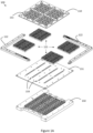
- FIGS 1A and 1B show antenna arrangements having a stacked layered structure.
- a stacked layered structure is a structure comprising a plurality of planar elements referred to as layers. Each planar element has two sides, or faces, and is associated with a thickness. The thickness is much smaller than the dimension of the faces, i.e., the layer is a flat or approximately planar element.
- a layer is rectangular or square. However, more general shapes are also applicable, including circular or elliptical disc shapes.
- the stacked layered structure is stacked in the sense that layers are arranged on top of each other. In other words, the layered structure can be seen as a sandwich structure.
- the antenna arrangement in Figure 1A comprises a radiation layer 110 with a plurality of radiation elements 111.
- the radiation elements are slot antennas.
- a slot antenna is an example of an aperture.
- a distribution layer 120 (shown in Figure 1B ) distributes one or more radio frequency signals to and from one or more radiation elements in the plurality of radiation elements.
- the distribution layer 120 can be based on electromagnetic bandgap, EBG, structures, which present compact designs, low loss, low leakage, and forgiving manufacturing and assembling tolerances.
- EBG electromagnetic bandgap
- manufacturing tolerances for EBG structures start to become challenging. This problem is especially severe for antenna arrays at millimeter wave frequencies which may comprise over a hundred radiation elements.
- EBG structures in the antenna arrangement are arranged to form at least one waveguide intermediate two layers.
- EBG structures are also arranged to prevent electromagnetic propagation (i.e. electromagnetic radiation) in a frequency band of operation from propagating along the layers except through the at least one wave guide.
- EBG structures may be arranged to prevent unwanted electromagnetic propagated between adjacent waveguides.
- the at least one waveguide couples the electromagnetic signal in the band of operation to one or more feeds and/or to one or more radiation elements.
- EBG structures prevent propagation by attenuation.
- to attenuate is interpreted as to significantly reduce an amplitude or power of electromagnetic radiation, such as a radio frequency signal.
- the attenuation is preferably complete, in which case attenuate and block are equivalent, but it is appreciated that such complete attenuation is not always possible to achieve.
- EBG structures form a surface that acts a magnetic conductor. If the magnetically conductive surface faces an electrically conductive surface, and if the two surfaces are arranged at a distance less than a quarter of a center frequency, no electromagnetic waves in the frequency band of operation can, in the ideal case, propagate along the intermediate surfaces, since all parallel plate modes are cut-off in that frequency band.
- the center frequency is in the middle of the frequency band of operation. In a realistic scenario, the electromagnetic waves in the frequency band of operation are attenuated per length along the intermediate surfaces.
- EBG structures There exists a multitude of EBG structures.
- the EBG elements of the EBG structure are arranged in a periodic or quasi-periodic pattern in one, two or three dimensions, as will be discussed in more detail below in connection to Figures 7A-D .
- a quasi-periodic pattern is interpreted to mean a pattern that is locally periodic but displays no long-range order.
- a quasi-periodic pattern may be realized in one, two or three dimensions.
- a quasi-periodic pattern can be periodic at length scales below ten times an EBG element spacing, but not at length scales over 100 times the EBG element spacing.
- An EBG structure may comprise at least two EBG element types, the first type of EBG element comprising an electrically conductive material and the second type of EBG element comprising an electrically insulating material.
- EBG elements of the first type may be made from a metal such as copper or aluminum, or from a non-conductive material like PTFE or FR-4 coated with a thin layer of an electrically conductive material like gold or copper.
- EBG elements of the first type may also be made from a material with an electric conductivity comparable to that of a metal, such as a carbon nanostructure or electrically conductive polymer. As an example, the electric conductivity of EBG elements of the first type can be above 10 3 Siemens per meter (S/m).
- the electric conductivity of EBG elements of the first type is above 10 5 S/m.
- the electric conductivity of EBG elements of the first type is high enough that the electromagnetic radiation can induce currents in the EBG elements of the first type
- the electric conductivity of EBG elements of the second type is low enough that no currents can be induced in EBG elements of the second type.
- EBG elements of the second type may optionally be non-conductive polymers, vacuum, or air. Examples of such non-conductive EBG element types also comprise FR-4 PCB material, PTFE, plastic, rubber, and silicon.
- EBG elements of the first and second type may be arranged in a pattern characterized by any of translational (701 in Figure 7A ), rotational (702 in Figure 7B ), or glide symmetry (see the symmetry line 703 in Figure 7C ), or a periodic, quasi-periodic or irregular pattern (see Figure 7D ).
- the physical properties of the EBG elements of the second type also determines the dimensions required to obtain attenuation of electromagnetic propagation past the EBG structure.
- the second type of material is chosen to be differently from air, the required dimensions of the first type of EBG element changes. Consequently, a reduced size antenna array can be obtained by varying the choice of material for the first and the second type of element.
- a reduced size antenna array may be obtained from such a choice.
- the EBG elements of the first type may be arranged in a periodic pattern with some spacing.
- the spaces between the EBG elements of the first type constitute the elements of the second type.
- the EBG elements of the first type are interleaved with EBG elements of the second type. Interleaving of the EBG elements of the first and second type can be achieved in one, two or three dimensions.
- a size of the EBG elements of either the first or the second type, or both, is smaller than the wavelength in air of electromagnetic radiation in the frequency band.
- the EBG element size is between 1/5th and 1/50th of the wavelength in air of electromagnetic radiation at the center frequency.
- the EBG element size is interpreted as the size of an EBG element in a direction where the electromagnetic waves are attenuated, e.g. along a surface that acts as a magnetic conductor.
- the size of the EBG element corresponds to a length or diameter of the cross-section of the rod.
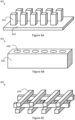
- FIGS 6A, 6B and 6C show examples of how EBG elements of the first and second type may be arranged in an EBG structure.
- a type of EBG structure 601, shown in Figure 6A comprises electrically conductive protrusions 610 on an electrically conductive substrate 620.
- the protrusions 610 may optionally be encased in a dielectric material.
- the electrically conductive protrusions constitute the EBG elements of the first type, and the spaces in-between the protrusions, optionally filled with a non-conductive material, constitute the EBG elements of the second type.
- the protrusions 610 may be formed in different shapes.
- Figure 6A shows an example where the protrusions have a square cross-section, but the protrusions may also be formed with a circular, elliptical, rectangular, or more generally shaped cross-section shape.
- the protrusions are mushroom shaped, as in, e.g. a cylindrical rod on an electrically conductive substrate with a flat electrically conductive circle on top of the rod, wherein the circle has a cross section larger than the cross section of the rod, but small enough to leave space for the second EBG element type between the circles in the EBG structures.
- Such mushroom-shaped protrusion may be formed in a PCB, wherein the rod comprises a via hole, which may or may not be filled with electrically conductive material.
- the protrusions have a length in a direction facing away from the electrically conductive substrate.
- the EBG element of the second type is air
- the protrusion length corresponds to a quarter of the wavelength in air at the center frequency.
- the surface along the tops of the protrusions is then close to a perfect magnetic conductor at the center frequency.
- this type of EBG structure still presents a band of frequencies where electromagnetic waves may be attenuated, when the EBG structure faces an electrically conductive surface.
- the center frequency is 15 GHz and electromagnetic waves in the frequency band 10 to 20 GHz propagating intermediate the EBG structure and the electrically conductive surface are attenuated.
- a type of EBG structure 602 shown in Figure 6B consists of a single slab of electrically conductive material 640 into which cavities 630 have been introduced.
- the cavities may be air-filled or filled with a non-conductive material. It is appreciated that the cavities may be formed in different shapes.
- Figure 6B shows an example where elliptical cross-section holes have been formed, but the holes may also be formed with circular, rectangular, or more general cross-section shapes.
- the slab 640 constitutes the EBG elements of the first type
- the holes 630 constitute the EBG elements of the second type.
- the length in a direction facing away from the electrically conductive substrate
- the length in a direction facing away from the electrically conductive substrate
- Figure 6C schematically illustrates a third exemplary type of EBG structure 603 consisting of extended electrically conductive EBG elements 650, optionally rods or slabs, stacked in multiple layers with the rods in a layer arranged at an angle to the rods in a previous layer.
- the rods constitute EBG elements of the first type and the spaces in between constitutes EBG elements of the second type.
- the example of Figure 6C shows an EBG structure where interleaving of EBG elements of the first and second type is achieved in three dimensions.
- the EBG element size decreases as the frequency increases and the number of EBG elements increases as the number of radiation elements increase.
- the yield can be low when mass producing such distribution layer. The more EBG elements and the smaller the size of the EBG elements, the worse the yield often is.
- the distribution layer 120 for a 16 x 16 radiation element antenna array comprises four distribution modules 121. Each of the four modules is arranged to distribute one or more radio frequency signals to and from one or more radiation elements 111 in a subset of radiation elements.
- the radiation elements comprise apertures and the subset of apertures comprises 8 x 8 apertures. If, for example, the yield is an exponentially decreasing function of the number of radiation elements, manufacturing four distribution modules 121 - for 8 x 8 radiation elements each - provides a better yield compared to manufacturing a single distribution layer - for 16 x 16 radiation elements.
- the antenna arrangement comprises a radiation layer 110 with one or more radiation elements 111, and a distribution layer 120 facing the radiation layer 110.
- the distribution layer 120 is arranged to distribute a radio frequency signal to the one or more radiation elements 111.
- the distribution layer 120 comprises at least one distribution layer feed 323 and a first electromagnetic bandgap, EBG, structure 324 arranged to form at least one first waveguide intermediate the distribution layer 120 and the radiation layer 110.
- the first EBG structure is also arranged to prevent electromagnetic propagation (i.e. electromagnetic radiation) in a frequency band of operation from propagating from the at least one first wave guide in directions other than through the at least one distribution layer feed 323 and the one or more radiation elements 111.
- the distribution layer comprises a plurality of distribution modules 121 and a positioning structure 122, wherein the positioning structure 122 is arranged to fix the distribution modules 121 in position.
- the distribution layer 120 is arranged with direct contact to the radiation layer 100 or is arranged at a distance from the radiation layer 110, where the distance is smaller than a quarter of a wavelength of center frequency of operation of the antenna arrangement 100.
- EBG structures in the distribution layer provides low losses from the waveguides as well as low interference between radio frequency signals in adjacent waveguides. A consequence of this is that a higher signal to noise ratio can be maintained due to the use and placement of EBG structures in the distribution layer, which is advantageous.
- Another advantage is that there is no need for electrical contact between the two layers constituting the waveguide. This is an advantage since high precision assembly is not necessary since electrical contact need not be verified.
- the positioning structure 122 optionally comprises a frame.
- the frame may hold the distribution layers in position by alignment taps, fastening means, or the like.
- Fastening means can be, e.g., bolts, screws, rivets, heat staking, glue, or the like. It is also possible that the frame holds the distribution modules in position without any alignment taps, fastening means, or the like.
- the radiation layer is also held in position by the frame. Alternatively, or in combination of, the distribution modules 121 and radiation layer 110 are attached together. Thus, the radiation layer may constitute the positioning structure 122.
- the frame 122 comprises a plurality of frame modules.
- the frame comprises two frame modules.
- the plurality of frame modules facilitates assembly of the antenna arrangement.
- the frame 122 is arranged to mate with distribution modules around a perimeter of the antenna arrangement 100.
- the frame preferably fits the modules snugly in position. This way, the modules are fixed with minimal play.
- the distribution modules 121 are arranged to be fixed in a common plane by the frame 122. This way, all distribution modules are arranged snugly against the radiation layer 110 or at the same distance from the radiation layer.
- the distribution modules are equally shaped, i.e. all of them are interchangeable in the antenna arrangement 100. This is an advantage from a manufacturing point of view since only one type of distribution module is required.
- the distribution modules may be shaped such that the total size of the antenna arrangement can be scaled. Examples of different scaling are arranging an array of 2 by 2 distribution modules or an array of 1 by 3 distribution modules.
- the distribution modules 121 preferably leave no gaps or minimal gaps between each other when arranged in position in the antenna arrangement. This way, it is possible to form a joint EBG structure in the distribution layer.
- the frame 122 is arranged to fill gaps between the distribution modules. No gaps between the distribution modules allows only the radio frequency signal in the frequency band of operation to pass through the distribution layer - through at least one first waveguide and the at least one distribution layer feed 323.
- Example dimensions of a rectangular distribution module are a thickness of 5 mm and sides 50 mm and 50 mm.
- the distribution modules are, however, not necessarily rectangular - other shapes are also possible, such as circular sectors to form a disc shaped or hexagonal shaped modules. It is also possible that the distribution layer modules have jigsaw puzzle shapes.
- the distribution modules may comprise metal, such as copper or brass, that has been casted, molded and/or machined.
- the metal may comprise a coating with high electrical conductivity, e.g. aluminum coated with silver or copper or zinc coated with silver or copper. It is also possible that each distribution module is metalized on a scaffold structure comprising, e.g., plastic.
- At least one of the one or more radiation elements 111 in the disclosed antenna arrangement 100 may comprise an aperture.
- An aperture of the radiation layer 110 may for example be a slot opening extending through the radiation layer.
- the slot opening is preferably rectangular, although other shapes such as square, round, or more general shapes are also possible.
- the slot openings are preferably small compared to the size of the radiation layer 110 and arranged in parallel lines on the radiation layer, although other arrangements are possible.
- the radiation layer 110 may, e.g., comprise a metal sheet (of e.g. copper).
- Another example of a radiating element is a bowtie antenna.
- a radiating element may be a patch antenna.
- both bowtie and patch antennas are easy to manufacture.
- the radiation layer 110 may, e.g., comprise a PCB with a ground plane, where the ground plane is facing the distribution layer. It is understood that other types of radiation elements are also possible.
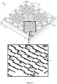
- FIG. 2 shows details of an assembled example antenna arrangement 100.
- Each distribution module 121 optionally comprises one or more alignment members 211.
- the one or more alignment members are arranged to align the module with respect to the other modules and with respect to the radiation elements 111.
- the one or more alignment members on the distribution modules 121 are arranged to mate with one or more corresponding alignment members.
- An alignment member and a corresponding alignment member may, e.g., be a pin and a hole.
- the one or more corresponding alignment members may be arranged on: adjacent distribution modules; the radiation layer 110; the frame 122; and/or on an optional support layer 130 arranged facing the distribution layer 120.
- one or more of alignment members are edge alignment members 211'.
- the one or more edge alignment members are arranged such that each distribution module 121 can only be assembled to the radiation layer 110 in a single and correct orientation.
- the one or more edge alignment members make the distribution modules rotationally asymmetric (in the plane extending along the distribution layer). This is an advantage in the assembling of the antenna arrangement 100.
- the alignment members may constitute part of the positioning structure.
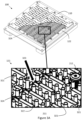
- FIGs 3A and 3B show details of the distribution layer 120 in an assembled example antenna arrangement 100.
- the first EBG structure 324 optionally comprises a repetitive structure of protruding elements 321.
- the distribution layer 120 optionally comprises at least one waveguide ridge 322, thereby forming at least one first gap waveguide intermediate the distribution layer 120 and the radiation layer 110. Details regarding EBG structures comprising protrusions is discussed above in relation to Figure 6A .
- ridge coupling transitions 324 are arranged intermediate the distribution feeds 323 and the waveguide ridges 322.
- the antenna arrangement 100 optionally comprises a support layer 130 facing the distribution layer 120.
- the support layer 130 is arranged to support the positioning structure 122 and/or the plurality of distribution modules 121. This way, the radiation layer and the distribution layer may securely be fixed together.
- the radiation layer may be attached to the frame and/or to the distribution layer by one or more bolts 212 (or the like). Alternatively, or in combination of, the one or more bolts may pass through the frame and/or through the distribution layer through respective holes, and the one or more bolts are attached to the support layer.
- each of the four distribution modules 121 is arranged to distribute one or more radio frequency signals to and from one or more radiation elements 111 in the respective subset of radiation elements.
- the subset of radiation elements comprises 8 x 8 radiation elements.
- the antenna arrangement comprise bolts intermediate the plurality of distribution modules, since that may fit the layers and plurality of distributions modules securely together.
- the support layer 130 optionally comprises a printed circuit board, PCB, layer 131 and a shield layer 132.
- the PCB layer comprises at least one PCB layer feed 133.
- the PCB layer in Figure 1A faces the distribution layer 120 and the shield layer 132 faces the PCB layer.
- EBG structures in the distribution layer enables highly efficient coupling at the transitions from the PCB layer feeds 133 on the PCB layer 131 through distribution feeds 323 to the at least one first waveguide, which results in low loss.
- the PCB layer 131 optionally comprises at least one RF integrated circuit (IC) arranged on either or both sides of the PCB layer.
- the at least one PCB layer feed 133 may be arranged to transfer radio frequency signals from the RF IC(s) to an opposite side of the PCB, into the distribution layer.
- the at least one PCB layer feed 133 is a through hole connected to a corresponding opening in the distribution layer 120, wherein the through hole is fed by at least one microstrip line.
- the at least one PCB layer feed 133 may be arranged to transfer radio frequency signals from RF IC(s) on the side of the PCB facing the distribution layer into the distribution layer.
- at least one PCB layer feed 133 is arranged to transfer radio frequency signals away the antenna arrangement 100, to, e.g., a modem.
- FIG. 4 shows details of an example shield layer 132.
- the shield layer 132 optionally comprises a second EBG structure 431 arranged to form at least one second waveguide intermediate the shield layer 132 and the PCB layer 131.
- the second EBG structure is also arranged to prevent electromagnetic propagation (i.e. electromagnetic radiation) in a frequency band of operation from propagating from the at least one second wave guide in directions other than through the at least one PCB layer feed 133.
- the second EBG structure allows a compact design with low loss and low leakage, i.e. unwanted electromagnetic propagation between, e.g., adjacent waveguides or between adjacent RFICs.
- the second EBG structure shields the PCB layer from electromagnetic radiation outside of the antenna arrangement.
- the second EBG structure 431 optionally comprises a repetitive structure of protruding elements 432,434, and the PCB layer optionally comprises a ground plane and at least one planar transmission line, thereby forming at least one second gap waveguide intermediate the shield layer 132 and the PCB layer 131.
- the at least one second gap waveguide may, e.g., be an inverted microstrip gap waveguide.
- the example shield layer of Figure 4 comprises two types of protruding elements 432,434.
- the narrow and tall pins 432 are examples of the protruding pins discussed above in relation to Figure 6A .
- the wider and shorter pins 434 are similar to the pins 432, except that they are adapted to fit RFICs between the shield layer and the PCB layer.
- the pins 434 may contact RFICs for heat transfer purposes.
- Figure 4 also shows screw mounting pins 433.
- the distribution layer 120 comprises a third EBG structure, which is arranged on the opposite side of the first EBG structure 324, i.e. the third EBG structure faces the support layer 130.
- the third EBG structure allows a compact design with low loss and low leakage, i.e. unwanted electromagnetic propagation between, e.g., adjacent waveguides or between adjacent RFICs.
- the third EBG structure shields the PCB layer from electromagnetic radiation outside of the antenna arrangement.
- the third EBG structure may comprise different pins similar to the pins of the second EBG structure in Figure 4 .
- the radiation layer 110 optionally comprises a plurality of radiation modules. This way, the yield of manufacturing the radiation layer might improve.
- the radiation modules can optionally be size matched to the distribution modules, which may facilitate assembly of the antenna arrangement. For example, in a 16 x 16 antenna array, a distribution module arranged to distribute radio signals to 8 x 8 radiation elements can be matched with a radiation module comprising 8 x 8 radiation elements.
- the radiation modules may be attached to the distribution layer and/or to the optional shield layer by bolts or the like.
- the frame 122 can be arranged to fix both the distribution modules and the radiation modules in position.
- the PCB layer 131 comprises a plurality of PCB modules and/or the shield layer 132 comprises a plurality of shield modules.
- all modules can be size matched to the distribution modules. This may facilitate assembly of the antenna arrangement.
- a distribution module arranged to distribute radio signals to 8 x 8 radiation elements can be matched with a radiation module comprising 8 x 8 radiation elements and matched with a PCB module and a shield module with matching sizes. All modules may be attached together by bolts or the like.
- the frame 122 can be arranged to fix all modules in position.
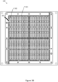
- Figure 5A shows a top view of an example antenna arrangement.
- Figure 5B shows a cross section view of the line A to B in Figure 5A .
- a telecommunication or radar transceiver comprises the antenna arrangement 100.
Landscapes
- Physics & Mathematics (AREA)
- Electromagnetism (AREA)
- Engineering & Computer Science (AREA)
- Manufacturing & Machinery (AREA)
- Optics & Photonics (AREA)
- Variable-Direction Aerials And Aerial Arrays (AREA)
- Waveguide Aerials (AREA)
- Waveguide Connection Structure (AREA)
- Waveguides (AREA)
Claims (12)
- Agencement d'antennes (100) ayant une structure en couches empilée, l'agencement d'antennes comprenant :une couche de rayonnement (110) comprenant un ou plusieurs éléments de rayonnement (111), et une couche de distribution (120) faisant face à la couche de rayonnement (110),dans lequel la couche de distribution (120) est agencée pour distribuer un signal de radiofréquence au ou aux éléments de rayonnement (111), la couche de distribution (120) comprenant au moins une alimentation de couche de distribution (323) et une première structure à bande interdite électromagnétique, EBG, (324) agencée pour former au moins un premier guide d'ondes entre la couche de distribution (120) et la couche de rayonnement (110), la première structure EBG est également conçue pour empêcher le rayonnement électromagnétique dans une bande de fréquences de fonctionnement de se propager à partir du ou des premiers guides d'ondes dans des directions autres que à travers la au moins une alimentation de couche de distribution (323) et le ou les éléments de rayonnement (111)caractérisé en ce quela couche de distribution comprend une pluralité de modules de distribution (121) et une structure de positionnement (122), dans lequel la structure de positionnement (122) est agencée pour fixer les modules de distribution (121) en position.
- Agencement d'antennes (100) selon la revendication 1, dans lequel la structure de positionnement (122) comprend un cadre.
- Agencement d'antennes (100) selon une quelconque des revendications précédentes, dans lequel au moins un du ou des plusieurs éléments de rayonnement comprend une ouverture.
- Agencement d'antennes (100) selon une quelconque des revendications précédentes, dans lequel la première structure EBG (324) comprend une structure répétitive d'éléments protubérants (321) et la couche de répartition (120) comprend en outre au moins une crête de guide d'ondes (322), formant ainsi au moins un premier guide d'ondes à espacement intermédiaire entre la couche de distribution (120) et la couche de rayonnement (110).
- Agencement d'antennes (100) selon une quelconque des revendications précédentes comprenant en outre une couche de support (130) faisant face à la couche de distribution (120), la couche de support (130) étant agencée pour soutenir la structure de positionnement (122) et/ou la pluralité de modules de distribution (121) .
- Agencement d'antennes (100) selon la revendication 5, dans lequel la couche de support (130) comprend une couche de carte de circuit imprimé, PCB, (131) et une couche de blindage (132), dans lequel la couche de PCB comprend au moins une couche de d'alimentation de PCB (133), et dans lequel la couche PCB fait face à la couche de distribution (120) et la couche de protection (132) fait face à la couche PCB.
- Agencement d'antennes (100) selon la revendication 6, dans lequel la couche de blindage (132) comprend une deuxième structure EBG (431) agencée pour former au moins un deuxième guide d'ondes entre la couche de blindage (132) et la couche PCB (131), la deuxième structure EBG étant également conçue pour empêcher que le rayonnement électromagnétique dans une bande de fréquence de fonctionnement se propage à partir du ou des deuxièmes guides d'ondes dans des directions autres que à travers la ou les alimentations de couche de PCB (133).
- Agencement d'antennes (100) selon la revendication 7, dans lequel la deuxième structure EBG (431) comprend une structure répétitive d'éléments protubérants (432, 434), et dans lequel la couche PCB comprend un plan de masse et au moins une ligne de transmission plane, formant ainsi au moins un deuxième guide d'ondes entre la couche de protection (132) et la couche PCB (131).
- Agencement d'antennes (100) selon une quelconque des revendications précédentes, dans lequel la couche de rayonnement (110) comprend une pluralité de modules de rayonnement.
- Agencement d'antennes (100) selon une quelconque des revendications 6 à 8, dans lequel la couche PCB (131) comprend une pluralité de modules PCB.
- Agencement d'antennes (100) selon une quelconque des revendications 6 à 8, dans lequel la couche de blindage (132) comprend une pluralité de modules de blindage.
- Emetteur-récepteur de télécommunication ou radar comprenant l'agencement d'antennes (100) selon une quelconque des revendications 1-11.
Applications Claiming Priority (2)
| Application Number | Priority Date | Filing Date | Title |
|---|---|---|---|
| SE2030028A SE2030028A1 (en) | 2020-01-31 | 2020-01-31 | A scalable modular antenna arrangement |
| PCT/EP2021/050433 WO2021151648A1 (fr) | 2020-01-31 | 2021-01-12 | Agencement d'antenne modulaire à échelle variable |
Publications (2)
| Publication Number | Publication Date |
|---|---|
| EP4097796A1 EP4097796A1 (fr) | 2022-12-07 |
| EP4097796B1 true EP4097796B1 (fr) | 2023-10-18 |
Family
ID=73543281
Family Applications (2)
| Application Number | Title | Priority Date | Filing Date |
|---|---|---|---|
| EP20811309.2A Pending EP4097795A1 (fr) | 2020-01-31 | 2020-11-20 | Agencements d'antenne et dispositifs à micro-ondes dotés de moyens de fixation améliorés |
| EP21700536.2A Active EP4097796B1 (fr) | 2020-01-31 | 2021-01-12 | Agencement d'antenne modulaire à échelle variable |
Family Applications Before (1)
| Application Number | Title | Priority Date | Filing Date |
|---|---|---|---|
| EP20811309.2A Pending EP4097795A1 (fr) | 2020-01-31 | 2020-11-20 | Agencements d'antenne et dispositifs à micro-ondes dotés de moyens de fixation améliorés |
Country Status (7)
| Country | Link |
|---|---|
| US (2) | US11978956B2 (fr) |
| EP (2) | EP4097795A1 (fr) |
| JP (3) | JP7743419B2 (fr) |
| KR (2) | KR102902463B1 (fr) |
| CN (2) | CN115298903A (fr) |
| SE (1) | SE2030028A1 (fr) |
| WO (2) | WO2021151538A1 (fr) |
Families Citing this family (8)
| Publication number | Priority date | Publication date | Assignee | Title |
|---|---|---|---|---|
| WO2022019148A1 (fr) * | 2020-07-21 | 2022-01-27 | ソニーセミコンダクタソリューションズ株式会社 | Dispositif d'antenne |
| US12401136B2 (en) * | 2020-12-22 | 2025-08-26 | A.D.S. International S.R.L. | Antenna and antenna system for satellite communications |
| CN112909545A (zh) * | 2021-03-10 | 2021-06-04 | 盛纬伦(深圳)通信技术有限公司 | 基于脊间隙波导的波导缝隙天线 |
| US11749884B2 (en) * | 2021-05-17 | 2023-09-05 | HJWAVE Co., Ltd. | Multi-layer antenna structure supporting wide band and wide angle |
| US11843178B1 (en) | 2023-05-23 | 2023-12-12 | Micro-Ant, LLC | Compact unit cell PCB antenna system with waveguide coupling |
| CN116995437B (zh) * | 2023-09-26 | 2024-04-26 | 华南理工大学 | 间隙波导天线及车载毫米波雷达 |
| CN119921072A (zh) * | 2023-10-23 | 2025-05-02 | 深圳引望智能技术有限公司 | 波导装置及相关产品 |
| DE102024210094A1 (de) | 2024-10-18 | 2026-04-23 | Robert Bosch Gesellschaft mit beschränkter Haftung | Radarsensor mit lasergelöteter Hohlleiterantenne und Verfahren zu dessen Herstellung |
Family Cites Families (24)
| Publication number | Priority date | Publication date | Assignee | Title |
|---|---|---|---|---|
| US3653052A (en) * | 1970-09-18 | 1972-03-28 | Nasa | Omnidirectional slot antenna for mounting on cylindrical space vehicle |
| JP2000013135A (ja) * | 1998-06-22 | 2000-01-14 | Yagi Antenna Co Ltd | スロットアレイアンテナ |
| CA2350352A1 (fr) * | 2001-06-13 | 2002-12-13 | Linda P.B. Katehi | Filtres planaires faisant appel a des substrats periodiques a bande interdite electromagnetique |
| US6995725B1 (en) * | 2002-11-04 | 2006-02-07 | Vivato, Inc. | Antenna assembly |
| US6947008B2 (en) * | 2003-01-31 | 2005-09-20 | Ems Technologies, Inc. | Conformable layered antenna array |
| US7639197B1 (en) * | 2006-07-28 | 2009-12-29 | Rockwell Collins, Inc. | Stacked dual-band electromagnetic band gap waveguide aperture for an electronically scanned array |
| US7348932B1 (en) * | 2006-09-21 | 2008-03-25 | Raytheon Company | Tile sub-array and related circuits and techniques |
| KR101066419B1 (ko) * | 2009-05-22 | 2011-09-23 | 한국조폐공사 | 전자기 밴드갭 패턴, 그 제조방법 및 전자기 밴드갭 패턴을 이용한 보안제품 |
| JP5590504B2 (ja) * | 2009-08-31 | 2014-09-17 | 日立化成株式会社 | トリプレート線路層間接続器及び平面アレーアンテナ |
| US8120543B2 (en) * | 2009-10-19 | 2012-02-21 | Oleksandr Sulima | Transmission line slot antenna |
| JP5289282B2 (ja) * | 2009-11-11 | 2013-09-11 | 三菱電機株式会社 | 平面アンテナ |
| US9407011B2 (en) * | 2012-02-22 | 2016-08-02 | The United States Of America As Represented By The Secretary Of The Army | Broadband electromagnetic band-gap (EBG) structure |
| CN110167255A (zh) * | 2013-03-15 | 2019-08-23 | 伟创力有限责任公司 | 用于创建完全微波吸收印刷电路板的方法和装置 |
| US10658758B2 (en) | 2014-04-17 | 2020-05-19 | The Boeing Company | Modular antenna assembly |
| JP6262617B2 (ja) * | 2014-08-08 | 2018-01-17 | 株式会社Soken | 表面電流抑制フィルタ及びアンテナ装置 |
| US10498000B2 (en) * | 2015-01-19 | 2019-12-03 | Gapwaves Ab | Microwave or millimeter wave RF part realized by die-forming |
| EP3147994B1 (fr) * | 2015-09-24 | 2019-04-03 | Gapwaves AB | Guides d'ondes et lignes de transmission dans des interstices entre des surfaces conductrices parallèles |
| DE102016125412B4 (de) * | 2015-12-24 | 2023-08-17 | Nidec Elesys Corporation | Schlitz-Array-Antenne und Radar, Radarsystem sowie Drahtlos-Kommunikationssystem mit der Schlitz-Array-Antenne |
| JP7020677B2 (ja) * | 2017-04-13 | 2022-02-16 | 日本電産エレシス株式会社 | スロットアンテナ装置 |
| CA3063768A1 (fr) * | 2017-05-15 | 2018-11-22 | Valorbec Societe En Commandite | Dispositifs et procedes pour guides d'ondes integres au substrat remplis d'air sans contact |
| CN107331974B (zh) * | 2017-06-05 | 2020-05-22 | 西安电子科技大学 | 一种基于脊间隙波导的圆极化天线 |
| ES2886940T3 (es) * | 2017-09-25 | 2021-12-21 | Gapwaves Ab | Red de antenas en fase |
| DE102018124924A1 (de) * | 2017-10-10 | 2019-04-11 | Nidec Corporation | Wellenleitende Vorrichtung |
| RU2696676C1 (ru) * | 2018-12-06 | 2019-08-05 | Самсунг Электроникс Ко., Лтд. | Гребневый волновод без боковых стенок на базе печатной платы и содержащая его многослойная антенная решетка |
-
2020
- 2020-01-31 SE SE2030028A patent/SE2030028A1/en not_active IP Right Cessation
- 2020-11-20 CN CN202080095109.1A patent/CN115298903A/zh active Pending
- 2020-11-20 US US17/796,362 patent/US11978956B2/en active Active
- 2020-11-20 JP JP2022546584A patent/JP7743419B2/ja active Active
- 2020-11-20 EP EP20811309.2A patent/EP4097795A1/fr active Pending
- 2020-11-20 KR KR1020227029826A patent/KR102902463B1/ko active Active
- 2020-11-20 WO PCT/EP2020/082921 patent/WO2021151538A1/fr not_active Ceased
-
2021
- 2021-01-12 EP EP21700536.2A patent/EP4097796B1/fr active Active
- 2021-01-12 WO PCT/EP2021/050433 patent/WO2021151648A1/fr not_active Ceased
- 2021-01-12 US US17/796,435 patent/US11978957B2/en active Active
- 2021-01-12 JP JP2022546579A patent/JP2023511764A/ja active Pending
- 2021-01-12 KR KR1020227029825A patent/KR20220141821A/ko not_active Withdrawn
- 2021-01-12 CN CN202180011493.7A patent/CN115280596A/zh active Pending
-
2025
- 2025-05-30 JP JP2025090851A patent/JP2025128216A/ja not_active Withdrawn
Also Published As
| Publication number | Publication date |
|---|---|
| US11978956B2 (en) | 2024-05-07 |
| JP2023511766A (ja) | 2023-03-22 |
| EP4097795A1 (fr) | 2022-12-07 |
| CN115280596A (zh) | 2022-11-01 |
| EP4097796A1 (fr) | 2022-12-07 |
| JP2023511764A (ja) | 2023-03-22 |
| KR102902463B1 (ko) | 2025-12-19 |
| US20230344144A1 (en) | 2023-10-26 |
| KR20220137925A (ko) | 2022-10-12 |
| SE543424C2 (en) | 2021-01-12 |
| US20230084399A1 (en) | 2023-03-16 |
| JP2025128216A (ja) | 2025-09-02 |
| US11978957B2 (en) | 2024-05-07 |
| CN115298903A (zh) | 2022-11-04 |
| KR20220141821A (ko) | 2022-10-20 |
| WO2021151648A1 (fr) | 2021-08-05 |
| WO2021151538A1 (fr) | 2021-08-05 |
| SE2030028A1 (en) | 2021-01-12 |
| JP7743419B2 (ja) | 2025-09-24 |
Similar Documents
| Publication | Publication Date | Title |
|---|---|---|
| EP4097796B1 (fr) | Agencement d'antenne modulaire à échelle variable | |
| EP4168820B1 (fr) | Antenne guide d'onde à fentes en ligne | |
| Tomura et al. | A 45$^\circ $ linearly polarized hollow-waveguide corporate-feed slot array antenna in the 60-GHz Band | |
| Su et al. | 79-GHz wide-beam microstrip patch antenna and antenna array for millimeter-wave applications | |
| JP2020108147A (ja) | アンテナ装置、レーダーシステム、および通信システム | |
| EP0410083A1 (fr) | Antenne à tente annulaire | |
| US12482952B2 (en) | Rotated ridge waveguide antenna | |
| US20250183544A1 (en) | A transition arrangement for a transition between two ridge gap waveguides | |
| CN116666980A (zh) | 毫米波宽波束dra、宽角波束扫描相控阵及其设计方法 | |
| SE544295C2 (en) | Contactless millimetre-wave array antenna element | |
| CN110931968A (zh) | 一种低交叉极化的毫米波微带平板阵列天线 | |
| CN212542648U (zh) | 一种右旋圆极化天线 | |
| CN113972482A (zh) | 基于色散结构的基片集成端射天线 | |
| Toshev | Synthesized shaped beam flat array antenna for digital beam-forming radar applications, utilizing printed technology | |
| CN222601366U (zh) | 毫米波雷达天线和雷达设备 | |
| CN119009489A (zh) | 一种天线结构和电子设备 | |
| KR200324767Y1 (ko) | 도파관용 슬롯 안테나 | |
| SE2130275A1 (en) | A circuit board-to-waveguide transition with an h-plane-fed patch antenna |
Legal Events
| Date | Code | Title | Description |
|---|---|---|---|
| STAA | Information on the status of an ep patent application or granted ep patent |
Free format text: STATUS: UNKNOWN |
|
| STAA | Information on the status of an ep patent application or granted ep patent |
Free format text: STATUS: THE INTERNATIONAL PUBLICATION HAS BEEN MADE |
|
| PUAI | Public reference made under article 153(3) epc to a published international application that has entered the european phase |
Free format text: ORIGINAL CODE: 0009012 |
|
| STAA | Information on the status of an ep patent application or granted ep patent |
Free format text: STATUS: REQUEST FOR EXAMINATION WAS MADE |
|
| 17P | Request for examination filed |
Effective date: 20220617 |
|
| AK | Designated contracting states |
Kind code of ref document: A1 Designated state(s): AL AT BE BG CH CY CZ DE DK EE ES FI FR GB GR HR HU IE IS IT LI LT LU LV MC MK MT NL NO PL PT RO RS SE SI SK SM TR |
|
| DAV | Request for validation of the european patent (deleted) | ||
| DAX | Request for extension of the european patent (deleted) | ||
| GRAP | Despatch of communication of intention to grant a patent |
Free format text: ORIGINAL CODE: EPIDOSNIGR1 |
|
| STAA | Information on the status of an ep patent application or granted ep patent |
Free format text: STATUS: GRANT OF PATENT IS INTENDED |
|
| INTG | Intention to grant announced |
Effective date: 20230524 |
|
| GRAS | Grant fee paid |
Free format text: ORIGINAL CODE: EPIDOSNIGR3 |
|
| GRAA | (expected) grant |
Free format text: ORIGINAL CODE: 0009210 |
|
| STAA | Information on the status of an ep patent application or granted ep patent |
Free format text: STATUS: THE PATENT HAS BEEN GRANTED |
|
| AK | Designated contracting states |
Kind code of ref document: B1 Designated state(s): AL AT BE BG CH CY CZ DE DK EE ES FI FR GB GR HR HU IE IS IT LI LT LU LV MC MK MT NL NO PL PT RO RS SE SI SK SM TR |
|
| REG | Reference to a national code |
Ref country code: GB Ref legal event code: FG4D |
|
| REG | Reference to a national code |
Ref country code: CH Ref legal event code: EP |
|
| REG | Reference to a national code |
Ref country code: IE Ref legal event code: FG4D |
|
| REG | Reference to a national code |
Ref country code: DE Ref legal event code: R096 Ref document number: 602021006024 Country of ref document: DE |
|
| REG | Reference to a national code |
Ref country code: LT Ref legal event code: MG9D |
|
| REG | Reference to a national code |
Ref country code: NL Ref legal event code: MP Effective date: 20231018 |
|
| REG | Reference to a national code |
Ref country code: AT Ref legal event code: MK05 Ref document number: 1623305 Country of ref document: AT Kind code of ref document: T Effective date: 20231018 |
|
| PG25 | Lapsed in a contracting state [announced via postgrant information from national office to epo] |
Ref country code: NL Free format text: LAPSE BECAUSE OF FAILURE TO SUBMIT A TRANSLATION OF THE DESCRIPTION OR TO PAY THE FEE WITHIN THE PRESCRIBED TIME-LIMIT Effective date: 20231018 |
|
| PG25 | Lapsed in a contracting state [announced via postgrant information from national office to epo] |
Ref country code: GR Free format text: LAPSE BECAUSE OF FAILURE TO SUBMIT A TRANSLATION OF THE DESCRIPTION OR TO PAY THE FEE WITHIN THE PRESCRIBED TIME-LIMIT Effective date: 20240119 |
|
| PG25 | Lapsed in a contracting state [announced via postgrant information from national office to epo] |
Ref country code: IS Free format text: LAPSE BECAUSE OF FAILURE TO SUBMIT A TRANSLATION OF THE DESCRIPTION OR TO PAY THE FEE WITHIN THE PRESCRIBED TIME-LIMIT Effective date: 20240218 |
|
| PG25 | Lapsed in a contracting state [announced via postgrant information from national office to epo] |
Ref country code: LT Free format text: LAPSE BECAUSE OF FAILURE TO SUBMIT A TRANSLATION OF THE DESCRIPTION OR TO PAY THE FEE WITHIN THE PRESCRIBED TIME-LIMIT Effective date: 20231018 |
|
| PG25 | Lapsed in a contracting state [announced via postgrant information from national office to epo] |
Ref country code: AT Free format text: LAPSE BECAUSE OF FAILURE TO SUBMIT A TRANSLATION OF THE DESCRIPTION OR TO PAY THE FEE WITHIN THE PRESCRIBED TIME-LIMIT Effective date: 20231018 |
|
| PG25 | Lapsed in a contracting state [announced via postgrant information from national office to epo] |
Ref country code: ES Free format text: LAPSE BECAUSE OF FAILURE TO SUBMIT A TRANSLATION OF THE DESCRIPTION OR TO PAY THE FEE WITHIN THE PRESCRIBED TIME-LIMIT Effective date: 20231018 |
|
| PG25 | Lapsed in a contracting state [announced via postgrant information from national office to epo] |
Ref country code: LT Free format text: LAPSE BECAUSE OF FAILURE TO SUBMIT A TRANSLATION OF THE DESCRIPTION OR TO PAY THE FEE WITHIN THE PRESCRIBED TIME-LIMIT Effective date: 20231018 Ref country code: IS Free format text: LAPSE BECAUSE OF FAILURE TO SUBMIT A TRANSLATION OF THE DESCRIPTION OR TO PAY THE FEE WITHIN THE PRESCRIBED TIME-LIMIT Effective date: 20240218 Ref country code: GR Free format text: LAPSE BECAUSE OF FAILURE TO SUBMIT A TRANSLATION OF THE DESCRIPTION OR TO PAY THE FEE WITHIN THE PRESCRIBED TIME-LIMIT Effective date: 20240119 Ref country code: ES Free format text: LAPSE BECAUSE OF FAILURE TO SUBMIT A TRANSLATION OF THE DESCRIPTION OR TO PAY THE FEE WITHIN THE PRESCRIBED TIME-LIMIT Effective date: 20231018 Ref country code: BG Free format text: LAPSE BECAUSE OF FAILURE TO SUBMIT A TRANSLATION OF THE DESCRIPTION OR TO PAY THE FEE WITHIN THE PRESCRIBED TIME-LIMIT Effective date: 20240118 Ref country code: AT Free format text: LAPSE BECAUSE OF FAILURE TO SUBMIT A TRANSLATION OF THE DESCRIPTION OR TO PAY THE FEE WITHIN THE PRESCRIBED TIME-LIMIT Effective date: 20231018 Ref country code: PT Free format text: LAPSE BECAUSE OF FAILURE TO SUBMIT A TRANSLATION OF THE DESCRIPTION OR TO PAY THE FEE WITHIN THE PRESCRIBED TIME-LIMIT Effective date: 20240219 |
|
| PG25 | Lapsed in a contracting state [announced via postgrant information from national office to epo] |
Ref country code: SE Free format text: LAPSE BECAUSE OF FAILURE TO SUBMIT A TRANSLATION OF THE DESCRIPTION OR TO PAY THE FEE WITHIN THE PRESCRIBED TIME-LIMIT Effective date: 20231018 Ref country code: RS Free format text: LAPSE BECAUSE OF FAILURE TO SUBMIT A TRANSLATION OF THE DESCRIPTION OR TO PAY THE FEE WITHIN THE PRESCRIBED TIME-LIMIT Effective date: 20231018 Ref country code: PL Free format text: LAPSE BECAUSE OF FAILURE TO SUBMIT A TRANSLATION OF THE DESCRIPTION OR TO PAY THE FEE WITHIN THE PRESCRIBED TIME-LIMIT Effective date: 20231018 Ref country code: NO Free format text: LAPSE BECAUSE OF FAILURE TO SUBMIT A TRANSLATION OF THE DESCRIPTION OR TO PAY THE FEE WITHIN THE PRESCRIBED TIME-LIMIT Effective date: 20240118 Ref country code: LV Free format text: LAPSE BECAUSE OF FAILURE TO SUBMIT A TRANSLATION OF THE DESCRIPTION OR TO PAY THE FEE WITHIN THE PRESCRIBED TIME-LIMIT Effective date: 20231018 Ref country code: HR Free format text: LAPSE BECAUSE OF FAILURE TO SUBMIT A TRANSLATION OF THE DESCRIPTION OR TO PAY THE FEE WITHIN THE PRESCRIBED TIME-LIMIT Effective date: 20231018 |
|
| PG25 | Lapsed in a contracting state [announced via postgrant information from national office to epo] |
Ref country code: DK Free format text: LAPSE BECAUSE OF FAILURE TO SUBMIT A TRANSLATION OF THE DESCRIPTION OR TO PAY THE FEE WITHIN THE PRESCRIBED TIME-LIMIT Effective date: 20231018 |
|
| REG | Reference to a national code |
Ref country code: DE Ref legal event code: R097 Ref document number: 602021006024 Country of ref document: DE |
|
| PG25 | Lapsed in a contracting state [announced via postgrant information from national office to epo] |
Ref country code: CZ Free format text: LAPSE BECAUSE OF FAILURE TO SUBMIT A TRANSLATION OF THE DESCRIPTION OR TO PAY THE FEE WITHIN THE PRESCRIBED TIME-LIMIT Effective date: 20231018 |
|
| PG25 | Lapsed in a contracting state [announced via postgrant information from national office to epo] |
Ref country code: SK Free format text: LAPSE BECAUSE OF FAILURE TO SUBMIT A TRANSLATION OF THE DESCRIPTION OR TO PAY THE FEE WITHIN THE PRESCRIBED TIME-LIMIT Effective date: 20231018 |
|
| PG25 | Lapsed in a contracting state [announced via postgrant information from national office to epo] |
Ref country code: SM Free format text: LAPSE BECAUSE OF FAILURE TO SUBMIT A TRANSLATION OF THE DESCRIPTION OR TO PAY THE FEE WITHIN THE PRESCRIBED TIME-LIMIT Effective date: 20231018 Ref country code: SK Free format text: LAPSE BECAUSE OF FAILURE TO SUBMIT A TRANSLATION OF THE DESCRIPTION OR TO PAY THE FEE WITHIN THE PRESCRIBED TIME-LIMIT Effective date: 20231018 Ref country code: RO Free format text: LAPSE BECAUSE OF FAILURE TO SUBMIT A TRANSLATION OF THE DESCRIPTION OR TO PAY THE FEE WITHIN THE PRESCRIBED TIME-LIMIT Effective date: 20231018 Ref country code: IT Free format text: LAPSE BECAUSE OF FAILURE TO SUBMIT A TRANSLATION OF THE DESCRIPTION OR TO PAY THE FEE WITHIN THE PRESCRIBED TIME-LIMIT Effective date: 20231018 Ref country code: EE Free format text: LAPSE BECAUSE OF FAILURE TO SUBMIT A TRANSLATION OF THE DESCRIPTION OR TO PAY THE FEE WITHIN THE PRESCRIBED TIME-LIMIT Effective date: 20231018 Ref country code: DK Free format text: LAPSE BECAUSE OF FAILURE TO SUBMIT A TRANSLATION OF THE DESCRIPTION OR TO PAY THE FEE WITHIN THE PRESCRIBED TIME-LIMIT Effective date: 20231018 Ref country code: CZ Free format text: LAPSE BECAUSE OF FAILURE TO SUBMIT A TRANSLATION OF THE DESCRIPTION OR TO PAY THE FEE WITHIN THE PRESCRIBED TIME-LIMIT Effective date: 20231018 |
|
| PLBE | No opposition filed within time limit |
Free format text: ORIGINAL CODE: 0009261 |
|
| STAA | Information on the status of an ep patent application or granted ep patent |
Free format text: STATUS: NO OPPOSITION FILED WITHIN TIME LIMIT |
|
| PG25 | Lapsed in a contracting state [announced via postgrant information from national office to epo] |
Ref country code: MC Free format text: LAPSE BECAUSE OF FAILURE TO SUBMIT A TRANSLATION OF THE DESCRIPTION OR TO PAY THE FEE WITHIN THE PRESCRIBED TIME-LIMIT Effective date: 20231018 |
|
| PG25 | Lapsed in a contracting state [announced via postgrant information from national office to epo] |
Ref country code: MC Free format text: LAPSE BECAUSE OF FAILURE TO SUBMIT A TRANSLATION OF THE DESCRIPTION OR TO PAY THE FEE WITHIN THE PRESCRIBED TIME-LIMIT Effective date: 20231018 |
|
| REG | Reference to a national code |
Ref country code: CH Ref legal event code: PL |
|
| PG25 | Lapsed in a contracting state [announced via postgrant information from national office to epo] |
Ref country code: LU Free format text: LAPSE BECAUSE OF NON-PAYMENT OF DUE FEES Effective date: 20240112 |
|
| 26N | No opposition filed |
Effective date: 20240719 |
|
| PG25 | Lapsed in a contracting state [announced via postgrant information from national office to epo] |
Ref country code: LU Free format text: LAPSE BECAUSE OF NON-PAYMENT OF DUE FEES Effective date: 20240112 |
|
| PG25 | Lapsed in a contracting state [announced via postgrant information from national office to epo] |
Ref country code: BE Free format text: LAPSE BECAUSE OF NON-PAYMENT OF DUE FEES Effective date: 20240131 |
|
| PG25 | Lapsed in a contracting state [announced via postgrant information from national office to epo] |
Ref country code: FR Free format text: LAPSE BECAUSE OF NON-PAYMENT OF DUE FEES Effective date: 20240131 |
|
| PG25 | Lapsed in a contracting state [announced via postgrant information from national office to epo] |
Ref country code: CH Free format text: LAPSE BECAUSE OF NON-PAYMENT OF DUE FEES Effective date: 20240131 |
|
| PG25 | Lapsed in a contracting state [announced via postgrant information from national office to epo] |
Ref country code: SI Free format text: LAPSE BECAUSE OF FAILURE TO SUBMIT A TRANSLATION OF THE DESCRIPTION OR TO PAY THE FEE WITHIN THE PRESCRIBED TIME-LIMIT Effective date: 20231018 |
|
| PG25 | Lapsed in a contracting state [announced via postgrant information from national office to epo] |
Ref country code: SI Free format text: LAPSE BECAUSE OF FAILURE TO SUBMIT A TRANSLATION OF THE DESCRIPTION OR TO PAY THE FEE WITHIN THE PRESCRIBED TIME-LIMIT Effective date: 20231018 Ref country code: FR Free format text: LAPSE BECAUSE OF NON-PAYMENT OF DUE FEES Effective date: 20240131 Ref country code: CH Free format text: LAPSE BECAUSE OF NON-PAYMENT OF DUE FEES Effective date: 20240131 Ref country code: BE Free format text: LAPSE BECAUSE OF NON-PAYMENT OF DUE FEES Effective date: 20240131 |
|
| REG | Reference to a national code |
Ref country code: BE Ref legal event code: MM Effective date: 20240131 |
|
| PG25 | Lapsed in a contracting state [announced via postgrant information from national office to epo] |
Ref country code: IE Free format text: LAPSE BECAUSE OF NON-PAYMENT OF DUE FEES Effective date: 20240112 |
|
| PG25 | Lapsed in a contracting state [announced via postgrant information from national office to epo] |
Ref country code: IE Free format text: LAPSE BECAUSE OF NON-PAYMENT OF DUE FEES Effective date: 20240112 |
|
| PG25 | Lapsed in a contracting state [announced via postgrant information from national office to epo] |
Ref country code: CY Free format text: LAPSE BECAUSE OF FAILURE TO SUBMIT A TRANSLATION OF THE DESCRIPTION OR TO PAY THE FEE WITHIN THE PRESCRIBED TIME-LIMIT; INVALID AB INITIO Effective date: 20210112 |
|
| PG25 | Lapsed in a contracting state [announced via postgrant information from national office to epo] |
Ref country code: HU Free format text: LAPSE BECAUSE OF FAILURE TO SUBMIT A TRANSLATION OF THE DESCRIPTION OR TO PAY THE FEE WITHIN THE PRESCRIBED TIME-LIMIT; INVALID AB INITIO Effective date: 20210112 |
|
| GBPC | Gb: european patent ceased through non-payment of renewal fee |
Effective date: 20250112 |
|
| PG25 | Lapsed in a contracting state [announced via postgrant information from national office to epo] |
Ref country code: FI Free format text: LAPSE BECAUSE OF FAILURE TO SUBMIT A TRANSLATION OF THE DESCRIPTION OR TO PAY THE FEE WITHIN THE PRESCRIBED TIME-LIMIT Effective date: 20231019 |
|
| PG25 | Lapsed in a contracting state [announced via postgrant information from national office to epo] |
Ref country code: GB Free format text: LAPSE BECAUSE OF NON-PAYMENT OF DUE FEES Effective date: 20250112 |
|
| PG25 | Lapsed in a contracting state [announced via postgrant information from national office to epo] |
Ref country code: TR Free format text: LAPSE BECAUSE OF FAILURE TO SUBMIT A TRANSLATION OF THE DESCRIPTION OR TO PAY THE FEE WITHIN THE PRESCRIBED TIME-LIMIT Effective date: 20231018 |
|
| PGFP | Annual fee paid to national office [announced via postgrant information from national office to epo] |
Ref country code: DE Payment date: 20251209 Year of fee payment: 6 |