EP4099092B1 - Procédé lithographique destiné à l'estampage des microstructures tridimensionnelles à des hauteurs de structure surdimensionnées dans un matériau porteur - Google Patents
Procédé lithographique destiné à l'estampage des microstructures tridimensionnelles à des hauteurs de structure surdimensionnées dans un matériau porteur Download PDFInfo
- Publication number
- EP4099092B1 EP4099092B1 EP21177401.3A EP21177401A EP4099092B1 EP 4099092 B1 EP4099092 B1 EP 4099092B1 EP 21177401 A EP21177401 A EP 21177401A EP 4099092 B1 EP4099092 B1 EP 4099092B1
- Authority
- EP
- European Patent Office
- Prior art keywords
- carrier material
- exposure
- height
- partial
- virtual
- Prior art date
- Legal status (The legal status is an assumption and is not a legal conclusion. Google has not performed a legal analysis and makes no representation as to the accuracy of the status listed.)
- Active
Links
Images


Classifications
-
- G—PHYSICS
- G03—PHOTOGRAPHY; CINEMATOGRAPHY; ANALOGOUS TECHNIQUES USING WAVES OTHER THAN OPTICAL WAVES; ELECTROGRAPHY; HOLOGRAPHY
- G03F—PHOTOMECHANICAL PRODUCTION OF TEXTURED OR PATTERNED SURFACES, e.g. FOR PRINTING, FOR PROCESSING OF SEMICONDUCTOR DEVICES; MATERIALS THEREFOR; ORIGINALS THEREFOR; APPARATUS SPECIALLY ADAPTED THEREFOR
- G03F7/00—Photomechanical, e.g. photolithographic, production of textured or patterned surfaces, e.g. printing surfaces; Materials therefor, e.g. comprising photoresists; Apparatus specially adapted therefor
- G03F7/0037—Production of three-dimensional images
-
- G—PHYSICS
- G03—PHOTOGRAPHY; CINEMATOGRAPHY; ANALOGOUS TECHNIQUES USING WAVES OTHER THAN OPTICAL WAVES; ELECTROGRAPHY; HOLOGRAPHY
- G03F—PHOTOMECHANICAL PRODUCTION OF TEXTURED OR PATTERNED SURFACES, e.g. FOR PRINTING, FOR PROCESSING OF SEMICONDUCTOR DEVICES; MATERIALS THEREFOR; ORIGINALS THEREFOR; APPARATUS SPECIALLY ADAPTED THEREFOR
- G03F7/00—Photomechanical, e.g. photolithographic, production of textured or patterned surfaces, e.g. printing surfaces; Materials therefor, e.g. comprising photoresists; Apparatus specially adapted therefor
- G03F7/0035—Multiple processes, e.g. applying a further resist layer on an already in a previously step, processed pattern or textured surface
-
- G—PHYSICS
- G03—PHOTOGRAPHY; CINEMATOGRAPHY; ANALOGOUS TECHNIQUES USING WAVES OTHER THAN OPTICAL WAVES; ELECTROGRAPHY; HOLOGRAPHY
- G03F—PHOTOMECHANICAL PRODUCTION OF TEXTURED OR PATTERNED SURFACES, e.g. FOR PRINTING, FOR PROCESSING OF SEMICONDUCTOR DEVICES; MATERIALS THEREFOR; ORIGINALS THEREFOR; APPARATUS SPECIALLY ADAPTED THEREFOR
- G03F7/00—Photomechanical, e.g. photolithographic, production of textured or patterned surfaces, e.g. printing surfaces; Materials therefor, e.g. comprising photoresists; Apparatus specially adapted therefor
- G03F7/0005—Production of optical devices or components in so far as characterised by the lithographic processes or materials used therefor
-
- G—PHYSICS
- G03—PHOTOGRAPHY; CINEMATOGRAPHY; ANALOGOUS TECHNIQUES USING WAVES OTHER THAN OPTICAL WAVES; ELECTROGRAPHY; HOLOGRAPHY
- G03F—PHOTOMECHANICAL PRODUCTION OF TEXTURED OR PATTERNED SURFACES, e.g. FOR PRINTING, FOR PROCESSING OF SEMICONDUCTOR DEVICES; MATERIALS THEREFOR; ORIGINALS THEREFOR; APPARATUS SPECIALLY ADAPTED THEREFOR
- G03F7/00—Photomechanical, e.g. photolithographic, production of textured or patterned surfaces, e.g. printing surfaces; Materials therefor, e.g. comprising photoresists; Apparatus specially adapted therefor
- G03F7/26—Processing photosensitive materials; Apparatus therefor
- G03F7/30—Imagewise removal using liquid means
-
- G—PHYSICS
- G03—PHOTOGRAPHY; CINEMATOGRAPHY; ANALOGOUS TECHNIQUES USING WAVES OTHER THAN OPTICAL WAVES; ELECTROGRAPHY; HOLOGRAPHY
- G03F—PHOTOMECHANICAL PRODUCTION OF TEXTURED OR PATTERNED SURFACES, e.g. FOR PRINTING, FOR PROCESSING OF SEMICONDUCTOR DEVICES; MATERIALS THEREFOR; ORIGINALS THEREFOR; APPARATUS SPECIALLY ADAPTED THEREFOR
- G03F7/00—Photomechanical, e.g. photolithographic, production of textured or patterned surfaces, e.g. printing surfaces; Materials therefor, e.g. comprising photoresists; Apparatus specially adapted therefor
- G03F7/70—Microphotolithographic exposure; Apparatus therefor
- G03F7/70008—Production of exposure light, i.e. light sources
-
- G—PHYSICS
- G03—PHOTOGRAPHY; CINEMATOGRAPHY; ANALOGOUS TECHNIQUES USING WAVES OTHER THAN OPTICAL WAVES; ELECTROGRAPHY; HOLOGRAPHY
- G03F—PHOTOMECHANICAL PRODUCTION OF TEXTURED OR PATTERNED SURFACES, e.g. FOR PRINTING, FOR PROCESSING OF SEMICONDUCTOR DEVICES; MATERIALS THEREFOR; ORIGINALS THEREFOR; APPARATUS SPECIALLY ADAPTED THEREFOR
- G03F7/00—Photomechanical, e.g. photolithographic, production of textured or patterned surfaces, e.g. printing surfaces; Materials therefor, e.g. comprising photoresists; Apparatus specially adapted therefor
- G03F7/70—Microphotolithographic exposure; Apparatus therefor
- G03F7/70216—Mask projection systems
- G03F7/70283—Mask effects on the imaging process
- G03F7/70291—Addressable masks, e.g. spatial light modulators [SLMs], digital micro-mirror devices [DMDs] or liquid crystal display [LCD] patterning devices
-
- G—PHYSICS
- G03—PHOTOGRAPHY; CINEMATOGRAPHY; ANALOGOUS TECHNIQUES USING WAVES OTHER THAN OPTICAL WAVES; ELECTROGRAPHY; HOLOGRAPHY
- G03F—PHOTOMECHANICAL PRODUCTION OF TEXTURED OR PATTERNED SURFACES, e.g. FOR PRINTING, FOR PROCESSING OF SEMICONDUCTOR DEVICES; MATERIALS THEREFOR; ORIGINALS THEREFOR; APPARATUS SPECIALLY ADAPTED THEREFOR
- G03F7/00—Photomechanical, e.g. photolithographic, production of textured or patterned surfaces, e.g. printing surfaces; Materials therefor, e.g. comprising photoresists; Apparatus specially adapted therefor
- G03F7/70—Microphotolithographic exposure; Apparatus therefor
- G03F7/70383—Direct write, i.e. pattern is written directly without the use of a mask by one or multiple beams
-
- G—PHYSICS
- G03—PHOTOGRAPHY; CINEMATOGRAPHY; ANALOGOUS TECHNIQUES USING WAVES OTHER THAN OPTICAL WAVES; ELECTROGRAPHY; HOLOGRAPHY
- G03F—PHOTOMECHANICAL PRODUCTION OF TEXTURED OR PATTERNED SURFACES, e.g. FOR PRINTING, FOR PROCESSING OF SEMICONDUCTOR DEVICES; MATERIALS THEREFOR; ORIGINALS THEREFOR; APPARATUS SPECIALLY ADAPTED THEREFOR
- G03F7/00—Photomechanical, e.g. photolithographic, production of textured or patterned surfaces, e.g. printing surfaces; Materials therefor, e.g. comprising photoresists; Apparatus specially adapted therefor
- G03F7/70—Microphotolithographic exposure; Apparatus therefor
- G03F7/70416—2.5D lithography
-
- G—PHYSICS
- G03—PHOTOGRAPHY; CINEMATOGRAPHY; ANALOGOUS TECHNIQUES USING WAVES OTHER THAN OPTICAL WAVES; ELECTROGRAPHY; HOLOGRAPHY
- G03F—PHOTOMECHANICAL PRODUCTION OF TEXTURED OR PATTERNED SURFACES, e.g. FOR PRINTING, FOR PROCESSING OF SEMICONDUCTOR DEVICES; MATERIALS THEREFOR; ORIGINALS THEREFOR; APPARATUS SPECIALLY ADAPTED THEREFOR
- G03F7/00—Photomechanical, e.g. photolithographic, production of textured or patterned surfaces, e.g. printing surfaces; Materials therefor, e.g. comprising photoresists; Apparatus specially adapted therefor
- G03F7/70—Microphotolithographic exposure; Apparatus therefor
- G03F7/70483—Information management; Active and passive control; Testing; Wafer monitoring, e.g. pattern monitoring
- G03F7/70491—Information management, e.g. software; Active and passive control, e.g. details of controlling exposure processes or exposure tool monitoring processes
- G03F7/705—Modelling or simulating from physical phenomena up to complete wafer processes or whole workflow in wafer productions
-
- G—PHYSICS
- G03—PHOTOGRAPHY; CINEMATOGRAPHY; ANALOGOUS TECHNIQUES USING WAVES OTHER THAN OPTICAL WAVES; ELECTROGRAPHY; HOLOGRAPHY
- G03F—PHOTOMECHANICAL PRODUCTION OF TEXTURED OR PATTERNED SURFACES, e.g. FOR PRINTING, FOR PROCESSING OF SEMICONDUCTOR DEVICES; MATERIALS THEREFOR; ORIGINALS THEREFOR; APPARATUS SPECIALLY ADAPTED THEREFOR
- G03F7/00—Photomechanical, e.g. photolithographic, production of textured or patterned surfaces, e.g. printing surfaces; Materials therefor, e.g. comprising photoresists; Apparatus specially adapted therefor
- G03F7/70—Microphotolithographic exposure; Apparatus therefor
- G03F7/70483—Information management; Active and passive control; Testing; Wafer monitoring, e.g. pattern monitoring
- G03F7/70491—Information management, e.g. software; Active and passive control, e.g. details of controlling exposure processes or exposure tool monitoring processes
- G03F7/70508—Data handling in all parts of the microlithographic apparatus, e.g. handling pattern data for addressable masks or data transfer to or from different components within the exposure apparatus
-
- G—PHYSICS
- G03—PHOTOGRAPHY; CINEMATOGRAPHY; ANALOGOUS TECHNIQUES USING WAVES OTHER THAN OPTICAL WAVES; ELECTROGRAPHY; HOLOGRAPHY
- G03F—PHOTOMECHANICAL PRODUCTION OF TEXTURED OR PATTERNED SURFACES, e.g. FOR PRINTING, FOR PROCESSING OF SEMICONDUCTOR DEVICES; MATERIALS THEREFOR; ORIGINALS THEREFOR; APPARATUS SPECIALLY ADAPTED THEREFOR
- G03F7/00—Photomechanical, e.g. photolithographic, production of textured or patterned surfaces, e.g. printing surfaces; Materials therefor, e.g. comprising photoresists; Apparatus specially adapted therefor
- G03F7/70—Microphotolithographic exposure; Apparatus therefor
- G03F7/70483—Information management; Active and passive control; Testing; Wafer monitoring, e.g. pattern monitoring
- G03F7/7055—Exposure light control in all parts of the microlithographic apparatus, e.g. pulse length control or light interruption
- G03F7/70558—Dose control, i.e. achievement of a desired dose
-
- G—PHYSICS
- G03—PHOTOGRAPHY; CINEMATOGRAPHY; ANALOGOUS TECHNIQUES USING WAVES OTHER THAN OPTICAL WAVES; ELECTROGRAPHY; HOLOGRAPHY
- G03F—PHOTOMECHANICAL PRODUCTION OF TEXTURED OR PATTERNED SURFACES, e.g. FOR PRINTING, FOR PROCESSING OF SEMICONDUCTOR DEVICES; MATERIALS THEREFOR; ORIGINALS THEREFOR; APPARATUS SPECIALLY ADAPTED THEREFOR
- G03F9/00—Registration or positioning of originals, masks, frames, photographic sheets or textured or patterned surfaces, e.g. automatically
- G03F9/70—Registration or positioning of originals, masks, frames, photographic sheets or textured or patterned surfaces, e.g. automatically for microlithography
- G03F9/7003—Alignment type or strategy, e.g. leveling, global alignment
Definitions
- the invention relates to a lithographic method for embossing three-dimensional microstructures with large structure heights in a photostructurable carrier material.
- microstructures have recently found numerous new fields of application, for example in the areas of optoelectronics, photonics, image processing sensors, in the field of machine vision, robotics and in motion control systems.
- 2.5D - Microstructures can be molded into a carrier material.
- the person skilled in the art understands the term “2.5D” to be objects or structures which are three-dimensional (3D) per se but do not have a defined lower edge.
- 2.5D microstructures can have undercuts, undercuts and/or overhangs.
- spherical lenses that are rounded at their bottom edges are referred to as 2.5D structures.
- Such 2.5D microstructures can be used for optical applications, for example.
- the term structural height of the microstructure is also to be understood as meaning structural depth of the microstructure.
- a planar microstructure with a length in the X-axis direction and a width in the Y-axis direction can be specified.
- the structure heights of the microstructure are given in the Z-axis direction, which is used for height indication.
- Indentations or cavities in the microstructure, which can be measured from a surface level, can also be defined as structure depths in negative Z-axis direction.
- structure heights are mostly used in the following.
- the disadvantage here is that due to the light absorption increasing exponentially with the layer thickness of the photoresist, the penetration depth during exposure of the photoresist is severely limited. Associated with this, the possible maximum structural height or structural depth with which the photoresist can be structured is also subject to the same limitation.
- an increase in the light dose i.e. the light intensity per exposed area, can lead to the destruction of the photoresist above a certain limit.
- Positive photoresists currently available on the market can usually be exposed with a light dose of at most 1200 mWs/cm 2 . When using a single layer of a positive photoresist, the production of microstructures is therefore limited to a maximum structure height or structure depth of at most 100 ⁇ m (micrometers).
- 2PL direct two-photon laser beam lithography
- voxel a combination of the abbreviation syllables "vox" for "volume” and “el” for “elements” refers to a grid point or image point in a three-dimensional grid.
- voxel denotes the discrete value at an XYZ coordinate of the data set.
- a disadvantage of this method which can also be used to produce 2.5D and real 3D structures with structure heights in the millimeter range, is the very slow writing speed of currently only around 3 mm 2 per hour.
- the layer height of each individual written structure layer corresponds to a voxel size, i.e. the size of a pixel of less than one micrometer ( ⁇ m).
- This technique is therefore limited to total areas to be structured of at most a few square millimeters.
- the processing time is too slow, such microstructures can be produced neither efficiently nor inexpensively and only with low throughput.
- a third technology that is already known is the diamond turning technique, which, however, is basically limited to the production of rotationally symmetrical objects.
- Ultra-precision diamond turning technology which was actually developed for structuring 3D structures on a micrometer scale, also has weaknesses. For example, the structures of workpieces manufactured using ultra-precision diamond turning technology usually deviate from the specified structural shape on a micrometer scale. Deviations of up to 3 micrometers ( ⁇ m) are common, which is why diamond turning technology is not suitable for the precise structuring of microstructures.
- DE10 2008 006438A1 discloses a lithography process for the production of 3D structures, in which a single photoresist layer is exposed in layers. However, there is only a single development step after the complete exposure of all layers. DE10 2008 006438A1 discloses a thickness of the photoresist layer of 10 ⁇ m, ie the overall height of the microstructure produced is significantly smaller than the maximum nominal penetration depth of the electromagnetic radiation.
- US2019/278005A1 discloses a lithography process for generating 3D microstructures, in which (thin) photoresist layers are applied, exposed and developed iteratively.
- US2010/099051A1 discloses a lithography method for producing 3D microstructures, in which a layer of photoresist that is thicker (20 ⁇ m) than the focus depth of the laser direct writer used is exposed in layers. However, there is only a single development step following full exposure.
- WO2021/071484A1 discloses a lithographic method for controlling edge angles in which a single layer of photoresist is exposed and developed layer by layer.
- the layer-by-layer development of the layers that have already been exposed is WO2021/071484A1 shown as one possibility only, a single development process following full exposure is disclosed as an alternative.
- the present invention therefore sets itself the task of providing an improved lithographic To specify a method for embossing three-dimensional microstructures, which have large structural heights, in a carrier material.
- the new method is intended to overcome the disadvantages known from the prior art: Especially in comparison to one-photon laser beam lithography (1PL method), it should be possible with the new method to be able to produce microstructures with a structure height or structure depth of more than 100 micrometers ( ⁇ m) quickly and with high precision.
- excessive structure height is understood here to mean microstructures whose structure heights are greater than the maximum nominal penetration depth of the exposure into a photostructurable carrier material.
- a maximum nominal penetration depth of the exposure that corresponds to the currently available materials and devices is about 100 microns ( ⁇ m) maximum nominal penetration depth.
- a 4x microscope objective with a numerical aperture of 0.14 as the exposure device. It can also be useful, for example, to select a light dose of 750 mWs/cm 2 in order to achieve an exposure depth of about 50 micrometers ( ⁇ m) in the photostructurable carrier material at a light wavelength of 405 nanometers using maskless one-photon laser beam lithography (1PL for short). (nm) and at a writing speed of 100 mm/s.
- the development time it can be advantageous, for example, to choose a development time of 30 minutes, in particular if, for example, the product AZ® 2026 MIF Developer from Microchemicals (www.microchemicals.com) is used as the developer.
- oversized structure heights are defined as heights that are greater than the recommended value of about 100 micrometers ( ⁇ m) mentioned and that can also be significantly greater than this guide value. Structures can also be advantageously embossed or written into the photostructurable carrier material with the method according to the invention, the structure heights of which can be, for example, in the order of magnitude of 500 micrometers ( ⁇ m) or more. Such oversized structure heights are also referred to below as structure heights on a sub-millimetre (mm) scale.
- a photostructurable carrier material is first applied over the entire surface of a substrate carrier.
- the photostructurable carrier material can be a photoresist, which if necessary is applied in several layers one on top of the other until there is a correspondingly large layer height of the planar carrier material, which is correspondingly larger than the oversized structure heights of the three-dimensional microstructure to be embossed, which are to be transferred to the carrier material.
- the photostructurable carrier material can be applied once or several times to the substrate carrier using one of the following common coating methods: dip coating; spin coating; slot die coating; Doctor blading, curtain coating or metering rod or Meyer bar coating.
- step -b- corresponding information for the subsequent modeling of the three-dimensional microstructure is collected based on the maximum nominal penetration depth during exposure of the selected carrier material and based on the geometric shape, in particular contour data, of the microstructure to be embossed, which has oversized structure heights.
- Step -c- can expediently be carried out using CAD files (Computer Aided Design), which are generated from the three-dimensional microstructure to be impressed as a virtual or digital three-dimensional structural model depending on the information previously determined.
- the virtual structural model includes topographical data of the microstructure to be molded, where an overall height of the structural model for the microstructure to be molded is determined on the basis of the topography data. This overall height of the structural model is greater than the maximum nominal penetration depth of the electromagnetic radiation during exposure into the carrier material and smaller than the applied layer height of the carrier material.
- topography (from Greek: tópos, “place”, and grafe ⁇ n, “to draw” or “describe”; literally “description of place”) is used below to describe the surface condition or the description of both the geometric shape and the physical and chemical properties of technical surfaces or microstructures understood.
- the description of the topography (surface roughness, surface shape, etc.) is usually based on data from measurement methods.
- the subdivision into at least two or more height layers of the virtual structure model stacked one on top of the other takes place in the Z-axis direction according to the height position of a Cartesian coordinate system.
- the next step -e- the calculation of a virtual photomask for each of the partial structures of the virtual structure model, preferably serves to control a device for maskless gray tone lithography.
- Each virtual photomask thus represents the individual exposure dose or the light intensity for a specific location of the partial structure.
- a maximum structural height of a specific location of the respective elevation or partial structure of the structural model corresponds to a maximum depth with which this location of the partial structure can be embossed or inscribed in the carrier material.
- the inversion of a structural height of the corresponding partial structure of the structural model into a structural depth of the structuring of this partial structure in the carrier material results from the photochemical structuring.
- the layer thickness that can be developed usually increases non-linearly with the exposure dose or light intensity per unit of time [in mWs/cm 2 ].
- step -f- a first virtual photomask, which corresponds to the first partial structure in the lowest height layer of the structure model, wherein in the first virtual photomask there are also alignment marks for impressing on the Surface of the carrier material are deposited, positioned accordingly on the surface of the carrier material.
- the carrier material is exposed in an aligned manner using the alignment markings that are arranged on the surface of the carrier material, with the first partial structure being structured starting from the surface of the carrier material by spatially resolved exposure in accordance with the individual exposure dose specified in the first virtual photomask is written into the carrier material.
- step -h- the wet-chemical development of the exposed section of the carrier material specified by the first virtual photomask takes place, with the surfaces of the structuring of the first partial structure depending on a selected structuring strategy, namely depending on the development rate of the carrier material used and smoothed by the calculated exposure dose until the surfaces of the structure are optically smooth after exposure and development.
- optically smooth surface is known to those skilled in the field of molding processes, in particular for the production of optical components. Such as the reference book “Optical measurement technology on technical surfaces” by Alexander W. Koch et al., expert-Verlag 1998, ISBN 3-8169-1372-5 , can be taken, a surface is referred to as “optically smooth” if its surface roughness or structure is far below the wavelength ⁇ (lambda) of the visible spectral range of light. For optically high-quality components, the requirement is maximum unevenness over an optically smooth surface of ⁇ /16.
- the criterion according to which the surfaces of the structure, i.e. the structured recess on the upper side of the carrier material, must be optically smooth after exposure and development has the effect that undesirable scattered light effects can be prevented in one or more subsequent exposure steps.
- the structuring of the surfaces in the structured recess or cavity within the carrier material is advantageously carried out in such a way that roughness values for the optically smooth surfaces are preferably less than or equal to 30 nm (nanometers).
- step -g- alignment of the process steps "aligned exposure”
- step -h- wet-chemical development
- the result of the structuring is therefore a structure written into the carrier material which has optically smooth surfaces which are suitable for one or more subsequent, further structuring steps.
- step -i- a first intermediate product of a partially structured carrier material is thus produced, the first intermediate product containing a structuring of the first partial structure.
- the further steps -j-, -k- and -1- are used for structuring a next virtual photomask corresponding to a subsequent, next height position of the virtual structure model within the structuring already produced beforehand.
- step -m- a sequence of steps -j- (positioning of a further virtual photomask), -k- (further exposure) and -1- (further development) is repeated as often as necessary until all virtual photomasks have been structured layer by layer.
- a finished structured carrier material is obtained according to the method as a product, the finished structured carrier material containing a structuring corresponding to the entire virtual three-dimensional structure model along its total height or together with its total height.
- the finished structured carrier material can further serve, for example, as a master for further molding of the original structure using galvanic methods or for the production of a stamp using silicone moulding.
- the photostructurable carrier material is a positive-working photoresist in which exposed sections are dissolved out of the carrier material during the subsequent wet-chemical development.
- Photoresists are used in photolithographic structuring, particularly in microelectronics and microsystems technology for the production of structures in the micrometer and submicrometer range and in the manufacture of printed circuit boards.
- the most important starting materials for photoresists are polymers (e.g. polymethyl methacrylate, polymethyl glutarimide) or epoxy resins, solvents such as cyclopentanone or gamma-butyrolactone, and a photo-sensitive component.
- the solubility of the photo layer is changed locally by the electromagnetic radiation in the form of the ultraviolet light component, which corresponds to the light dose of the virtual photo mask (photochemical reaction).
- the photoresist which may already have solidified, is photochemically altered by exposure to light and is therefore soluble for the appropriate developer solutions, and after development only the areas remain which have passed through a corresponding covering mask were protected from the irradiation or which are located outside the exposed sections.
- positive-working photoresist as a photostructurable carrier material offers the advantage that, according to the method, elevation layer by elevation layer - corresponding to the calculated virtual photomasks - can be structured deeper and deeper into the positive photoresist in order to finally create recesses or cavities in the finished structured positive photoresist to obtain whose total heights correspond to those of the given structural model.
- Non-structured areas of the positive-working photoresist which are therefore not exposed and developed, advantageously retain the layer height initially selected (according to step -a-).
- the ready-structured carrier material in the form of a positive-working photoresist can also be used, for example, as a master for further molding of the original structure using galvanic methods or for producing a stamp using silicone molding.
- the aligned exposure of the carrier material is carried out either by means of maskless laser lithography, which is based on 1-photon and/or 2-photon absorption, or by means of optical maskless lithography, using a spatial light modulator and imaging optics are used, is carried out.
- maskless laser lithography is understood by the person skilled in the art as a method for exposing the photostructurable carrier material, preferably the positive-working photoresist, with a focusing laser beam by means of sequential scanning and simultaneous modulation of the light intensity.
- Laser light is used as the exposure source.
- the advantages of this exposure method are that with maskless laser lithography, a particularly precisely defined light dose per pixel, i.e. at a location of the data set that is precisely defined using the XYZ coordinates. Due to the possibility of using one-photon absorption (abbreviated: 1PL) and/or two-photon absorption (abbreviated: 2PL), it is possible to produce real 3D structures with this exposure method. However, the disadvantage of this exposure method is that it tends to be slow due to the sequential scanning.
- 1PL one-photon absorption
- 2PL two-photon absorption
- optical maskless lithography is understood by the person skilled in the art as a method for exposing the photostructurable carrier material, preferably the positive-working one Photoresists in which the structuring takes place by optical imaging of a surface (pixel matrix) of a spatial light modulator on the carrier material or preferably the photoresist.
- UV light which is generated, for example, with UV LEDs, is used as the exposure source.
- the advantage of this exposure method is that the surface exposure can take place much faster than with maskless laser lithography.
- the disadvantage of the method of optical maskless lithography is that real 3D structuring with this exposure method can make it necessary to tilt the corresponding sample or the carrier material during structuring.
- it can be advantageous, in particular for structuring undercuts if at least one virtual photomask is positioned using alignment markings on the surface of a carrier material arranged tilted at a tilt angle.
- the carrier material may be necessary, in particular when using optical maskless lithography as an exposure method, to tilt the carrier material during the structuring of real 3D structures such as undercuts, undercuts and/or overhangs.
- the corresponding tilting angle at which the carrier material is tilted as required can be set, for example, by means of a motorized goniometer.
- the method according to the invention it is also possible for several or all of the virtual photomasks to be positioned on the surface of a carrier material arranged tilted at a tilt angle. Furthermore, it is provided within the scope of the method according to the invention that the carrier material for several or for all virtual photomasks can be tilted at the same tilt angle or at individual, different tilt angles for each elevation layer to be structured or for each virtual photomask.
- the aligned exposure of the substrate and the subsequent wet-chemical development of the exposed section of the substrate defined by the at least one virtual photomask can take place using alignment markings on the surface of a substrate arranged tilted at a tilt angle.
- the alignment markings which are also structured together with the first virtual photomask on the surface of the carrier material, are also used when the photomask is tilted Exposure or tilted structuring of the carrier material to precisely position the further, subsequent structuring steps.
- the photostructurable carrier material has a layer height greater than 100 micrometers ( ⁇ m), preferably greater than 200 micrometers ( ⁇ m), particularly preferably greater than 500 micrometers ( ⁇ m), with the carrier material preferably having multiple layers is applied to the substrate carrier.
- the layer height of the carrier material should be selected in such a way that the carrier material offers a sufficient layer thickness for accommodating the entire structural model, in particular the overall height of the structural model.
- the overall height of the structural model can advantageously be greater than 100 micrometers ( ⁇ m).
- the method according to the invention can advantageously be used to produce three-dimensional microstructures with oversized structure heights on a micrometer to sub-millimeter scale, which previously could not be produced quickly and precisely with the currently known production methods.
- the total height of the structure model, which is modeled in step -c- can therefore also be significantly greater than 100 micrometers ( ⁇ m) and reach a sub-millimeter scale.
- the number N (N ⁇ 2 to n) can be selected in the method such that each of the N (N ⁇ 2 to n) partial heights of the individual partial structures is less than or equal to a maximum nominal penetration depth, preferably less than 30 microns ( ⁇ m), more preferably less than 20 microns ( ⁇ m).
- the partial heights of the partial structures are selected to be less than or equal to 50 micrometers ( ⁇ m).
- the number N (N ⁇ 2 to n) is selected such that each of the N (N ⁇ 2 to n) partial heights of the individual partial structures has the same partial height, which partial height is less than or equal to one maximum nominal penetration depth is preferably less than 30 micrometers ( ⁇ m), more preferably less than 20 micrometers ( ⁇ m).
- the optically smooth surfaces of the partial structures after exposure and development have a roughness with an average roughness value Ra of at most 50 nanometers (nm), preferably at most 40 nanometers (nm), particularly preferably at most 30 nanometers (nm).
- optically smooth surfaces offer the advantage of being able to carry out the subsequent, further structuring without scattered light effects and thus without associated error sources.
- Fig.1 1 schematically shows a photostructurable carrier material 1, for example a positive-working photoresist, which is applied to a substrate carrier 2 in a plurality of flat layers 1.1, 1.2, 1.3,1.4 with a total layer height H.1.
- a substrate carrier 2 a flat glass plate is used here, for example.
- the several layers 1.1,1.2,1.3,1.4, from which the carrier material 1 is applied, are shown in a partial sectional view in FIG 1 symbolizes.
- the several layers 1.1, 1.2, 1.3, 1.4 of the positive-working photoresist combine with one another as homogeneously as possible in order to obtain a homogeneously structured carrier material 1 with a large layer height H.1, which has the same photochemical material properties at every location having.
- the layer height H.1 or layer thickness of the carrier material 1 or photoresist is chosen here to be 900 ⁇ m (microns), for example.
- the height direction of the layer height H.1 corresponds to the Z-axis direction.
- the base material 1 has a flat surface O.1 or outer surface, which extends in the direction of the XY plane.
- the product AZ® 4562 (“positive thick resist") or the product AZ® 9260, both from Microchemicals (www.microchemichals.com), can be used as the positive-working photoresist.
- a nominal maximum penetration depth of exposure for these photoresists is about 75 microns ( ⁇ m).
- the structural model 10 includes the topography data T.10 of the microstructure to be molded.
- the structural model 10 has an overall height H.10, which corresponds to the maximum extent of the structural model 10 in the Z-axis direction.
- the total height H.10 of the structural model 10 is 400 ⁇ m (micrometers) here, for example, and is therefore greater than the maximum nominal penetration depth of the electromagnetic radiation when exposing the carrier material (around 75 ⁇ m) and smaller than the applied layer height H.1 of 900 ⁇ m here Carrier material 1 on the substrate carrier 2.
- each substructure 11, 12, 13 has a partial height H.11, H.12, H.13, each of the Partial heights H.11, H.12, H.13 is less than or equal to the possible nominal penetration depth when the carrier material 1 is exposed.
- the same partial height H.11, H.12, H.13 is selected for each partial structure 11, 12, 13, which is 40 ⁇ m here, for example, and is therefore smaller than the nominal penetration depth when the carrier material 1 is exposed.
- the total height H.10 of 400 ⁇ m must be stacked on top of 10 Partial structures 11, 12, 13, etc. are divided, each of the partial structures here having the same partial height H.11, H.12, H.13, etc., for example, each of 40 ⁇ m.
- Each partial structure 11, 12, 13 has the associated topography data T.11, T.12, T.13.
- the representation in the following schematic illustrations is limited to the shown three partial structures 11, 12, 13 stacked one on top of the other to subdivide partial heights.
- FIG. 4 shows several virtual photo masks M.11, M.12, M.13, which are calculated for each of the partial structures 11, 12, 13 of the structural model 10.
- the respective topography data T.11, T.12, T.13 of the individual partial structures 11, 12, 13 or elevation layers of the structure model 10 are converted into corresponding values of an individual exposure dose.
- the tops of the substructures 11, 12, 13 labeled O.11, O.12 and O.13 serve here only for the clear assignment of how the individual substructures 11, 12, 13 are stacked one on top of the other in order to form the entire structural model 10 overall.
- photomasks M.11, M.12, M.13 correlate with the topography data T.11, T.12, T.13 of the individual substructures 11, 12, 13 insofar as that for a specific location X, Y, Z of a partial structure 11, 12, 13 is related to the associated individual altitude or to the coordinate value in the Z-axis direction of the same point X, Y, Z within this partial structure 11, 12, 13.
- figure 5 shows in a simplified diagram the correlation of the respective exposure dose I (in mWs/cm 2 ) of each virtual photomask M.11, M.12, M13 with the topographical data of each individual partial structure 11, 12, 13.
- the larger the local exposure dose I is selected the higher-lying locations X,Y,Z within a partial structure 11, 12, 13, the altitude of the locations relating to their position in the structure model 10, can be used in the subsequent structuring using the virtual photomasks M.11, M.12, M.13 are written all the deeper into the carrier material 1.
- a higher exposure dose I means that the carrier material 1 can be written all the more deeply.
- FIG. 6 shows the positioning of a first virtual photomask M.11, which corresponds to the first partial structure 11 of the lowest height layer of the structure model 10, together with alignment markings 20 on the surface O.1 of the carrier material 1 or the positive-working photoresists.
- the positioning of the photomask M.11 is symbolized here by an arrow A.
- the alignment markings 20, which are also used to align the subsequent method steps, are contained in the first virtual photomask M.11 and are also structured with it.
- an inverted first virtual photomask M'.11 is also shown.
- the inverted first virtual photomask M'.11 corresponds to the first virtual photomask M.11, but with changed or inverted polarity.
- the inversion of a structure height H.11 (in "positive” Z-axis direction according to 3 ) of the corresponding first partial structure 11 of the structural model 10 in a structural depth of the structuring S.11 of this partial structure 11 in the carrier material 1 (in the “negative” Z-axis direction according to 6 ) is due to the photochemical structuring.
- the structuring parameters are selected in such a way that the surfaces of the structuring S.11 are optically smooth G after structuring E than after exposure and development.
- Position 21 designates the first intermediate product 21 of the structured carrier material 1, which is structured with the structuring S.11 corresponding to the first partial structure 11.
- FIG. 7 illustrates after the exposure and development E of the carrier material 1 using the first virtual photomask M. 11 the positioning of a further, second virtual photomask M.12, which corresponds to the second partial structure 12 of the next higher height layer of the structure model 10, which sequentially follows the lowest height layer the already structured structuring S.11 of the first partial structure 11.
- the second virtual photomask M.12 is again positioned on the surface O.1 of the carrier material 1 using the alignment markings 20, which is symbolized by the arrow A.
- the further structuring which includes the aligned exposure of the exposed section of the carrier material 1 specified by the second virtual photomask M.12 and the subsequent wet-chemical development, is symbolized by the arrow E.
- Comparable to 7 is also in here 7 an inverted second virtual photomask M'.12 is shown.
- the inverted second virtual photomask M'.12 again corresponds to the second virtual photomask M.12, but with changed or inverted polarity.
- the inversion of the structure height H.12 (in "positive” Z-axis direction according to 3 ) of the corresponding second partial structure 12 of the structural model 10 in a structure depth of the structuring S.12 of this partial structure 12 in the carrier material 1 (in the “negative” Z-axis direction according to 7 ) is again due to photochemical structuring.
- the structuring parameters are selected in such a way that the surfaces of the structuring S.12, which is arranged inside or below the previously structured cavity S.11, are optically smooth G after the structuring E, than after the exposure and development.
- Position 22 designates the second intermediate product 22 of the structured carrier material 1, which is additionally structured with the structuring S.12 corresponding to the second partial structure 12.
- the inverted third virtual photomask M'.13 shown here corresponds to the third virtual photomask M.13, such as this in figure 5 is illustrated, but with changed or inverted polarity.
- the further structuring which includes the aligned exposure of the exposed section of the carrier material 1 specified by the third virtual photomask M.13 and the subsequent wet-chemical development, is again symbolized by the arrow E.
- the structuring parameters are selected in such a way that the surfaces of the structuring S.13, which is arranged inside or below the previously structured cavity S.12, are optically smooth G after the structuring E, than after the exposure and development.
- Position 23 designates the third intermediate product 23 of the structured carrier material 1, which is additionally already structured with the structuring S.13 corresponding to the third partial structure 13.
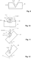
- FIG. 9 shows a side view of a finished structured carrier material 30 with a structuring of the entire in 2 structural model shown 10.
- FIG. 10 shows - comparable to 6 - the positioning of a first virtual photomask M.11, corresponding to the first partial structure 11 of the lowest level of a structural model 10 of a microstructure according to a second variant embodiment, together with alignment marks 20 on the surface of the support material 1.
- FIG. 11 shows the positioning of a further, second virtual photomask M.12 after structuring E, i.e. the exposure and development of the carrier material 1, corresponding to the first virtual photomask M.11, which corresponds to the second partial structure 12 of the next higher height layer sequentially following the lowest height layer
- Structural model 10 corresponds to a position tilted at a tilt angle ⁇ within the previously produced structuring S.11 of the first partial structure 11.
- the tilt angle ⁇ at which the carrier material 1 or here the first intermediate product 21 of the structured carrier material 1 is tilted is in relation to the horizontal, i.e. the XY plane in the Cartesian coordinate system.
- FIG. 12 shows a second intermediate product 22 in which the further second structuring S.12 has already been produced, which forms a three-dimensional undercut or an overhang of the structuring.
- the section of the undercut is in 12 marked with a two-dot chain line. If necessary, a completely structured carrier material with a structuring of a structural model with an overhang can be produced by appropriate repetition of further structuring steps.
Landscapes
- Physics & Mathematics (AREA)
- General Physics & Mathematics (AREA)
- Chemical & Material Sciences (AREA)
- Engineering & Computer Science (AREA)
- Materials Engineering (AREA)
- Manufacturing & Machinery (AREA)
- Exposure And Positioning Against Photoresist Photosensitive Materials (AREA)
- Mechanical Engineering (AREA)
- Optics & Photonics (AREA)
- Micromachines (AREA)
Claims (10)
- Procédé lithographique pour l'impression de microstructures tridimensionnelles, qui présentent des hauteurs de structure surdimensionnées, dans un matériau support photostructurable en utilisant un dispositif d'exposition, dans lequel, en fonction de paramètres d'exposition du dispositif d'exposition en relation avec des propriétés d'exposition du matériau de support photostructurable, une profondeur maximale de la bague nominale de l'exposition et donc une photostructuration résultante du matériau de support vont de pair et une hauteur de structure surdimensionnée présente une hauteur qui dépasse la valeur de la profondeur maximale de la bague nominale, le procédé comprenant les étapes de procédé suivantes :- a- application en surface d'un matériau support (1) pouvant être photostructuré sur un support de substrat (2), le matériau support (1) appliqué présentant une hauteur de couche (H.1) ainsi qu'une surface plane (O.1) sur la face supérieure opposée au support de substrat (2), et les propriétés du matériau support (1) pouvant être modifiées par exposition à un rayonnement électromagnétique ;- b- utilisation de données d'information comme grandeur d'entrée, ces données d'information contenant des indications sur la profondeur de pénétration nominale maximale du matériau support (1) photostructurable choisi ainsi que sur la forme géométrique d'une microstructure tridimensionnelle à imprimer présentant une hauteur de structure surdimensionnée ;- c- modélisation assistée par ordinateur d'un modèle structurel tridimensionnel virtuel (10) de la microstructure à gaufrer en fonction des données d'information selon l'étape -b-, le modèle structurel (10) comprenant des données topographiques (T.10) de la microstructure à gaufrer et, à l'aide des données topographiques (T.10), on détermine la hauteur de la microstructure à gaufrer. ), on détermine une hauteur totale (H.10) du modèle structurel (10) par rapport à la microstructure à mouler, laquelle hauteur totale (H.10) est supérieure à la profondeur de pénétration nominale maximale du rayonnement électromagnétique lors de l'exposition dans le matériau de support (1) et inférieure à la hauteur de couche appliquée (H.1) du matériau de support (1) ;- d- Subdivision assistée par ordinateur de la hauteur totale (H.10 ) du modèle structurel tridimensionnel (10) en un nombre N (N ≥ 2 à n) de couches de hauteur empilées séquentiellement les unes sur les autres, chacune des N (N ≥ 2 à n) couches de hauteur correspondant à une structure partielle individuelle (11, 12, 13,) du modèle structurel (10), et chacune des N (N ≥ 2 à n) structures partielles (11, 12, 13, ) ayant respectivement une hauteur partielle (H.11, H.12, H.13, ), le nombre N étant un nombre entier supérieur ou égal au nombre 2, et le nombre N (N ≥ 2 à n) étant choisi de telle sorte que chacune des N (N ≥ 2 à n) hauteurs partielles (H.11, H.12, H.13,) est inférieure ou égale à la profondeur d'anneau nominale possible du rayonnement électromagnétique pouvant être fourni par le dispositif d'exposition lors de l'exposition dans le matériau de support (1), la somme des N (N ≥ 2 à n) hauteurs partielles (H.11, H.12, H.13, ) des différentes structures partielles (11, 12, 13,) correspondant à la hauteur totale (H.10) du modèle de structure (10) ;- e- calculer un photomasque virtuel (M.11, M.12, M.13,) pour chacune des N (N ≥ 2 à n) sous-structures (11, 12, 13, ) du modèle structurel (10), dans lequel, pour chacun des N (N ≥ 2 à n) photomasques (M.11, M.12, M.13, ), les données topographiques respectives (T.11, T.12, T.13, ) de chaque sous-structure individuelle (11, 12, 13, ) sont converties en valeurs correspondantes d'une dose d'exposition individuelle, la dose d'exposition calculée pour un lieu déterminé (X, Y, Z) d'une sous-structure (11, 12, 13, ) étant corrélée avec l'altitude individuelle (Z) du même lieu (X, Y, Z) à l'intérieur de la sous-structure correspondante (11, 12, 13, ) ;- f- positionnement d'un premier photomasque virtuel (M.11) correspondant à la première structure partielle (11) dans la couche de hauteur la plus basse du modèle de structure (10), ainsi que de repères d'alignement (20) sur la surface (O.1) du matériau de support (1) ;- g- exposition orientée du matériau de support (1) à l'aide des repères d'orientation (20) qui sont disposés sur la surface (O.1), une structuration (S.11) de la première structure partielle (11) étant inscrite dans le matériau de support (1) à partir de la surface (O.1) du matériau de support (1) par exposition résolue en fonction de l'endroit (X, Y, Z) en fonction de la dose d'exposition individuelle définie dans le premier photomasque virtuel (M.11) ;- h- développement chimique par voie humide (E) de la section exposée du matériau support (1) prédéfinie par le premier photomasque virtuel (M.11), les surfaces de la structuration (S.11) de la première structure partielle (11) étant lissées en fonction d'un taux de développement du matériau support (1) ainsi que de la dose d'exposition calculée, jusqu'à ce que les surfaces de la structuration (S.11) soient optiquement lisses (G) après l'exposition et le développement (E) ;- i- obtenir un premier produit intermédiaire (21) d'un matériau de support partiellement structuré, le premier produit intermédiaire (21) contenant une structuration (S.11) de la première structure partielle (11) ;- j- positionner un autre Nte (N ≥ 2 à n) photomasque virtuel (M.12, M.13,), les Nte (N ≥ 2 à n) photomasques virtuels (M.12, M.13, ) de la Nte (N ≥ 2 à n) structure partielle (12, 13, ) dans la Nte (N ≥ 2 à n) couche de hauteur du modèle structurel (10) qui suit séquentiellement la (N-1) couche de hauteur respectivement précédente, correspond à l'intérieur de la structuration déjà structurée (S.11) de la (N-1) structure partielle (11) respectivement précédente du (N-1) produit intermédiaire (21) respectivement précédent ;- k- poursuite de l'exposition orientée du (N-1) produit intermédiaire (21, 22, 23, ) respectivement précédent à l'aide des repères d'orientation (20) qui sont disposés sur la surface (O.1), dans lequel, à partir de la structuration (S.11) déjà structurée de la (N-1) structure partielle (11) respectivement précédente, par exposition résolue en fonction de la position (X, Y, Z), conformément à la valeur d'exposition définie dans le Nième (N ≥ 2 à n) photomasque virtuel (M.12, M.13, ), une structuration (S.12, S.13, ) de la Nten (N ≥ 2 à n) structure partielle (12, 13, ) est inscrite dans le (N-1) produit intermédiaire (21) respectivement précédent d'un matériau support partiellement structuré, la structuration (S.12, S.13, ) de la nième (N ≥ 2 à n) structure partielle (12, 13, ) à l'intérieur du matériau support (1) est respectivement plus profonde que la structuration (5.11) de la (N-1) structure partielle (11) respectivement précédente ;- l- développement par voie chimique humide de la section exposée du matériau de support (1) prédéfinie par les Nte (N ≥ 2 à n) photomasques virtuels (M.12, M.13), les surfaces de la structuration (S.12, S.13, ) des N-ième (N ≥ 2 à n) sous-structures (12, 13, ) sont lissées en fonction d'un taux de développement du matériau support (1) ainsi que de la dose d'exposition calculée, jusqu'à ce que les surfaces de la structuration (5.11) soient optiquement lisses (G) après l'exposition et le développement (E) ;- m- si nécessaire, répéter en conséquence une séquence des étapes -j- (positionnement d'un autre photomasque virtuel à la fois), -k- (exposition supplémentaire) et -1- (développement supplémentaire) jusqu'à ce que tous les N (N ≥ 2 à n) photomasques virtuels (M.11, M.12, M.13, ) aient été structurés couche par couche ;- n- obtention d'un matériau support (30) structuré fini, le matériau support (30) structuré fini comprenant une structuration correspondant à l'ensemble du modèle de structure (S.10) et à sa hauteur totale (H.10).
- Procédé selon la revendication 1, caractérisé en ce que le matériau support (1) pouvant être photostructuré est une laque photosensible travaillant en positif, dans laquelle des sections exposées sont détachées du matériau support (1) lors du développement chimique humide suivant.
- Procédé selon la revendication 1 ou 2, caractérisé en ce que l'exposition alignée du matériau de support (1) est réalisée au moyen d'une lithographie laser sans masque, basée sur l'absorption d'un photon et/ou de deux photons, ou au moyen d'une lithographie optique sans masque, utilisant un modulateur spatial de lumière et une optique de formation d'image.
- Procédé selon l'une des revendications 1 à 3, caractérisé en ce qu'au moins un photomasque virtuel (M.11, M.12, M.13) est positionné à l'aide de repères d'alignement (20) sur la surface (O.1) d'un matériau support (1) incliné selon un angle d'inclinaison (α).
- Procédé selon la revendication 4, caractérisé en ce que l'exposition alignée du matériau de support (1) ainsi que le développement chimique humide (E) subséquent de la section exposée du matériau de support (1) prédéfinie par le au moins un photomasque virtuel (M.11, M.12, M.13) sont réalisés à l'aide de repères d'alignement (20) sur la surface (O.1) d'un matériau de support (1) disposé de manière inclinée sous un angle d'inclinaison (α).
- Procédé selon l'une des revendications 1 à 5, caractérisé en ce que le matériau support (1) photostructurable présente une hauteur de couche (H.1) supérieure à 100 µm, de préférence supérieure à 200 µm, de manière particulièrement préférée supérieure à 500 µm, le matériau support (1) étant de préférence déposé en plusieurs couches (1.1, 1.2, 1.3, 1.4) sur le support substrat (2).
- Procédé selon l'une des revendications 1 à 6, caractérisé en ce que la hauteur totale (H.10) du modèle structurel (10) est supérieure à 100 µm.
- Procédé selon l'une des revendications 1 à 7, caractérisé en ce que le nombre N (N ≥ 2 à n) est choisi de manière à ce que chacune des N (N ≥ 2 à n) hauteurs partielles (H.11, H.12, H.13) des différentes sous-structures (11, 12, 13) soit inférieure ou égale à une profondeur maximale de la gorge nominale, de préférence inférieure à 30 µm, de manière particulièrement préférée inférieure à 20 µm.
- Procédé selon l'une quelconque des revendications 1 à 8, caractérisé en ce que le nombre N (N ≥ 2 à n) est choisi de telle sorte que chacune des N (N ≥ 2 à n) hauteurs partielles (H.11, H.12, H.13) des différentes structures partielles (11, 12, 13) présente la même hauteur partielle, laquelle hauteur partielle est inférieure ou égale à une profondeur maximale de la gorge nominale, de préférence inférieure à 30 µm, de manière particulièrement préférée inférieure à 20 µm.
- Procédé selon l'une des revendications 1 à 9, caractérisé en ce que les surfaces optiquement lisses (G) des structures partielles (S.11, S.12, S.13) présentent, après l'exposition et le développement (E), une rugosité ayant une valeur de rugosité moyenne d'au plus 50 nm, de préférence d'au plus 40 nm, de manière particulièrement préférée d'au plus 30 nm.
Priority Applications (5)
| Application Number | Priority Date | Filing Date | Title |
|---|---|---|---|
| EP21177401.3A EP4099092B1 (fr) | 2021-06-02 | 2021-06-02 | Procédé lithographique destiné à l'estampage des microstructures tridimensionnelles à des hauteurs de structure surdimensionnées dans un matériau porteur |
| PCT/EP2022/063680 WO2022253591A1 (fr) | 2021-06-02 | 2022-05-20 | Procédé lithographique pour imprimer des microstructures tridimensionnelles à hauteurs structurales surdimensionnées dans un matériau support |
| US18/566,038 US12455503B2 (en) | 2021-06-02 | 2022-05-20 | Lithographic method for imprinting three-dimensional microstructures having oversized structural heights into a carrier material |
| JP2023574341A JP2024521896A (ja) | 2021-06-02 | 2022-05-20 | 過大構造高さを有する3次元微小構造を支持体材料に形成するためのリソグラフィ方法 |
| KR1020237040497A KR20240016263A (ko) | 2021-06-02 | 2022-05-20 | 초대형 구조 높이를 갖는 3차원 미세 구조를 캐리어 재료 내에 임프린트하기 위한 리소그래피 방법 |
Applications Claiming Priority (1)
| Application Number | Priority Date | Filing Date | Title |
|---|---|---|---|
| EP21177401.3A EP4099092B1 (fr) | 2021-06-02 | 2021-06-02 | Procédé lithographique destiné à l'estampage des microstructures tridimensionnelles à des hauteurs de structure surdimensionnées dans un matériau porteur |
Publications (2)
| Publication Number | Publication Date |
|---|---|
| EP4099092A1 EP4099092A1 (fr) | 2022-12-07 |
| EP4099092B1 true EP4099092B1 (fr) | 2023-03-15 |
Family
ID=76250208
Family Applications (1)
| Application Number | Title | Priority Date | Filing Date |
|---|---|---|---|
| EP21177401.3A Active EP4099092B1 (fr) | 2021-06-02 | 2021-06-02 | Procédé lithographique destiné à l'estampage des microstructures tridimensionnelles à des hauteurs de structure surdimensionnées dans un matériau porteur |
Country Status (5)
| Country | Link |
|---|---|
| US (1) | US12455503B2 (fr) |
| EP (1) | EP4099092B1 (fr) |
| JP (1) | JP2024521896A (fr) |
| KR (1) | KR20240016263A (fr) |
| WO (1) | WO2022253591A1 (fr) |
Family Cites Families (9)
| Publication number | Priority date | Publication date | Assignee | Title |
|---|---|---|---|---|
| US6255035B1 (en) * | 1999-03-17 | 2001-07-03 | Electron Vision Corporation | Method of creating optimal photoresist structures used in the manufacture of metal T-gates for high-speed semiconductor devices |
| JP2002107941A (ja) * | 2000-09-29 | 2002-04-10 | Seiko Epson Corp | 光加工方法、光加工装置、光デバイス、及びスタンパ |
| JP4206669B2 (ja) * | 2002-01-23 | 2009-01-14 | セイコーエプソン株式会社 | エッチングパターン形成方法 |
| DE102008006438B4 (de) * | 2008-01-28 | 2011-08-25 | Carl Zeiss SMT GmbH, 73447 | Verfahren und Vorrichtung zum Strukturieren eines strahlungsempfindlichen Materials |
| WO2010046408A2 (fr) * | 2008-10-22 | 2010-04-29 | Micronic Laser Systems Ab | Procédé de compensation itérative des effets non linéaires lors de l'exposition tridimensionnelle d'une résine photosensible |
| JP2010113270A (ja) * | 2008-11-10 | 2010-05-20 | Toppan Printing Co Ltd | 微小立体構造の製造方法及びそれに用いる露光用マスク |
| CN111819497B (zh) * | 2018-03-06 | 2024-02-27 | 应用材料公司 | 构建3d功能性光学材料堆叠结构的方法 |
| KR102808485B1 (ko) * | 2019-10-09 | 2025-05-14 | 어플라이드 머티어리얼스, 인코포레이티드 | 마스크리스 기반 리소그래피 방법들 |
| CN113515021A (zh) * | 2021-03-12 | 2021-10-19 | 苏州苏大维格科技集团股份有限公司 | 激光直写光刻机制作的三维微纳形貌结构 |
-
2021
- 2021-06-02 EP EP21177401.3A patent/EP4099092B1/fr active Active
-
2022
- 2022-05-20 WO PCT/EP2022/063680 patent/WO2022253591A1/fr not_active Ceased
- 2022-05-20 KR KR1020237040497A patent/KR20240016263A/ko active Pending
- 2022-05-20 JP JP2023574341A patent/JP2024521896A/ja active Pending
- 2022-05-20 US US18/566,038 patent/US12455503B2/en active Active
Also Published As
| Publication number | Publication date |
|---|---|
| EP4099092A1 (fr) | 2022-12-07 |
| WO2022253591A1 (fr) | 2022-12-08 |
| US20240248395A1 (en) | 2024-07-25 |
| JP2024521896A (ja) | 2024-06-04 |
| KR20240016263A (ko) | 2024-02-06 |
| US12455503B2 (en) | 2025-10-28 |
Similar Documents
| Publication | Publication Date | Title |
|---|---|---|
| DE3588184T2 (de) | Stereolithographische Vorrichtung und Verfahren zur Herstellung von dreidimensionalen Gegenständen | |
| EP2569140B1 (fr) | Dispositif et procédé de production de structures tridimensionnelles | |
| DE68927908T2 (de) | Verringerung des stereolithographischen Verbiegens | |
| EP3621766A1 (fr) | Procédé pour générer une structure 3d par lithographie au laser à l'aide d'une dose d'éclairage modifiée aux sections de bord ainsi que produit-programme informatique correspondant | |
| WO2005030430A1 (fr) | Procede et dispositif d'enlevement de matiere multicouche d'une surface tridimensionnelle par laser a l'aide d'un reseau de polygones qui est decrit par une fonction mathematique et represente la surface | |
| DE102006054820A1 (de) | Verfahren zur Korrektur von Platzierungsfehlern | |
| EP4086085A2 (fr) | Plaque d'estampage, procédé de fabrication et élément de sécurité estampé | |
| EP4099092B1 (fr) | Procédé lithographique destiné à l'estampage des microstructures tridimensionnelles à des hauteurs de structure surdimensionnées dans un matériau porteur | |
| DE102013108876A1 (de) | Fotolithografisches Verfahren zur Herstellung einer Struktur in einem Strahlung emittierenden Halbleiterbauelement | |
| DE102020107944B4 (de) | Verfahren zur Herstellung eines kontinuierlichen diffraktiven optischen Elementes und kontinuierliches diffraktives optisches Element | |
| DE112005002469T5 (de) | Festphasenimmersionslinsenlithographie | |
| DE10318105A1 (de) | Mikrostruktur und Verfahren zur Herstellung von Mikrostrukturen | |
| EP1763707B1 (fr) | Procédé poru réaliser des profiles dans des photorésistes | |
| AT520718B1 (de) | Verfahren zur herstellung eines formeinsatzes mit (sub-)mikrostrukturen sowie werkstück mit (sub-)mikrostrukturen | |
| WO2005030425A1 (fr) | Procede d'enlevement de matiere sur plusieurs couches dans une surface tridimensionnelle par l'utilisation d'une image matricielle decrivant la structure de surface | |
| US20220365261A1 (en) | Microstructure and method for manufacturing same | |
| EP3083251A1 (fr) | Procédé et dispositif de réalisation de surfaces structurées | |
| DE10146619C2 (de) | Verfahren zur Generation einer zweidimensionalen Photomaske | |
| WO2002037192A1 (fr) | Procede pour produire des hologrammes | |
| DE102015120535A1 (de) | Vorrichtung und Verfahren zur Herstellung einer beidseitig mikrostrukturierten Folie | |
| DE4435022A1 (de) | Grautonmaske für lithographische Strukturierungen von Bauelementen und Verfahren zu ihrer Herstellung | |
| DE102023105670A1 (de) | Prüfvorrichtung, verfahren zur herstellung einer schablone und prüfverfahren einer schablone | |
| EP4043186A1 (fr) | Procédé et dispositif de commande d'un dispositif de fabrication additive à base de lithographie | |
| EP4363197A1 (fr) | Gabarit structural pour la production d'un outil d'estampage pour l'estampage d'un élément en film mince, utilisation d'un gabarit structural et procédé de fourniture d'un gabarit structural | |
| DE102013208129A1 (de) | Mikrolithographische Projektionsbelichtungsanlage mit einem variablen Transmissionsfilter |
Legal Events
| Date | Code | Title | Description |
|---|---|---|---|
| PUAI | Public reference made under article 153(3) epc to a published international application that has entered the european phase |
Free format text: ORIGINAL CODE: 0009012 |
|
| STAA | Information on the status of an ep patent application or granted ep patent |
Free format text: STATUS: REQUEST FOR EXAMINATION WAS MADE |
|
| 17P | Request for examination filed |
Effective date: 20211207 |
|
| AK | Designated contracting states |
Kind code of ref document: A1 Designated state(s): AL AT BE BG CH CY CZ DE DK EE ES FI FR GB GR HR HU IE IS IT LI LT LU LV MC MK MT NL NO PL PT RO RS SE SI SK SM TR |
|
| GRAP | Despatch of communication of intention to grant a patent |
Free format text: ORIGINAL CODE: EPIDOSNIGR1 |
|
| STAA | Information on the status of an ep patent application or granted ep patent |
Free format text: STATUS: GRANT OF PATENT IS INTENDED |
|
| GRAS | Grant fee paid |
Free format text: ORIGINAL CODE: EPIDOSNIGR3 |
|
| GRAA | (expected) grant |
Free format text: ORIGINAL CODE: 0009210 |
|
| STAA | Information on the status of an ep patent application or granted ep patent |
Free format text: STATUS: THE PATENT HAS BEEN GRANTED |
|
| INTG | Intention to grant announced |
Effective date: 20230130 |
|
| AK | Designated contracting states |
Kind code of ref document: B1 Designated state(s): AL AT BE BG CH CY CZ DE DK EE ES FI FR GB GR HR HU IE IS IT LI LT LU LV MC MK MT NL NO PL PT RO RS SE SI SK SM TR |
|
| REG | Reference to a national code |
Ref country code: CH Ref legal event code: EP Ref country code: GB Ref legal event code: FG4D Free format text: NOT ENGLISH |
|
| REG | Reference to a national code |
Ref country code: DE Ref legal event code: R096 Ref document number: 502021000493 Country of ref document: DE |
|
| REG | Reference to a national code |
Ref country code: IE Ref legal event code: FG4D Free format text: LANGUAGE OF EP DOCUMENT: GERMAN |
|
| REG | Reference to a national code |
Ref country code: AT Ref legal event code: REF Ref document number: 1554348 Country of ref document: AT Kind code of ref document: T Effective date: 20230415 |
|
| P01 | Opt-out of the competence of the unified patent court (upc) registered |
Effective date: 20230524 |
|
| REG | Reference to a national code |
Ref country code: NL Ref legal event code: FP |
|
| REG | Reference to a national code |
Ref country code: LT Ref legal event code: MG9D |
|
| PG25 | Lapsed in a contracting state [announced via postgrant information from national office to epo] |
Ref country code: RS Free format text: LAPSE BECAUSE OF FAILURE TO SUBMIT A TRANSLATION OF THE DESCRIPTION OR TO PAY THE FEE WITHIN THE PRESCRIBED TIME-LIMIT Effective date: 20230315 Ref country code: NO Free format text: LAPSE BECAUSE OF FAILURE TO SUBMIT A TRANSLATION OF THE DESCRIPTION OR TO PAY THE FEE WITHIN THE PRESCRIBED TIME-LIMIT Effective date: 20230615 Ref country code: LV Free format text: LAPSE BECAUSE OF FAILURE TO SUBMIT A TRANSLATION OF THE DESCRIPTION OR TO PAY THE FEE WITHIN THE PRESCRIBED TIME-LIMIT Effective date: 20230315 Ref country code: LT Free format text: LAPSE BECAUSE OF FAILURE TO SUBMIT A TRANSLATION OF THE DESCRIPTION OR TO PAY THE FEE WITHIN THE PRESCRIBED TIME-LIMIT Effective date: 20230315 Ref country code: HR Free format text: LAPSE BECAUSE OF FAILURE TO SUBMIT A TRANSLATION OF THE DESCRIPTION OR TO PAY THE FEE WITHIN THE PRESCRIBED TIME-LIMIT Effective date: 20230315 |
|
| PG25 | Lapsed in a contracting state [announced via postgrant information from national office to epo] |
Ref country code: SE Free format text: LAPSE BECAUSE OF FAILURE TO SUBMIT A TRANSLATION OF THE DESCRIPTION OR TO PAY THE FEE WITHIN THE PRESCRIBED TIME-LIMIT Effective date: 20230315 Ref country code: GR Free format text: LAPSE BECAUSE OF FAILURE TO SUBMIT A TRANSLATION OF THE DESCRIPTION OR TO PAY THE FEE WITHIN THE PRESCRIBED TIME-LIMIT Effective date: 20230616 Ref country code: FI Free format text: LAPSE BECAUSE OF FAILURE TO SUBMIT A TRANSLATION OF THE DESCRIPTION OR TO PAY THE FEE WITHIN THE PRESCRIBED TIME-LIMIT Effective date: 20230315 |
|
| PG25 | Lapsed in a contracting state [announced via postgrant information from national office to epo] |
Ref country code: SM Free format text: LAPSE BECAUSE OF FAILURE TO SUBMIT A TRANSLATION OF THE DESCRIPTION OR TO PAY THE FEE WITHIN THE PRESCRIBED TIME-LIMIT Effective date: 20230315 Ref country code: RO Free format text: LAPSE BECAUSE OF FAILURE TO SUBMIT A TRANSLATION OF THE DESCRIPTION OR TO PAY THE FEE WITHIN THE PRESCRIBED TIME-LIMIT Effective date: 20230315 Ref country code: PT Free format text: LAPSE BECAUSE OF FAILURE TO SUBMIT A TRANSLATION OF THE DESCRIPTION OR TO PAY THE FEE WITHIN THE PRESCRIBED TIME-LIMIT Effective date: 20230717 Ref country code: ES Free format text: LAPSE BECAUSE OF FAILURE TO SUBMIT A TRANSLATION OF THE DESCRIPTION OR TO PAY THE FEE WITHIN THE PRESCRIBED TIME-LIMIT Effective date: 20230315 Ref country code: EE Free format text: LAPSE BECAUSE OF FAILURE TO SUBMIT A TRANSLATION OF THE DESCRIPTION OR TO PAY THE FEE WITHIN THE PRESCRIBED TIME-LIMIT Effective date: 20230315 Ref country code: CZ Free format text: LAPSE BECAUSE OF FAILURE TO SUBMIT A TRANSLATION OF THE DESCRIPTION OR TO PAY THE FEE WITHIN THE PRESCRIBED TIME-LIMIT Effective date: 20230315 |
|
| PG25 | Lapsed in a contracting state [announced via postgrant information from national office to epo] |
Ref country code: SK Free format text: LAPSE BECAUSE OF FAILURE TO SUBMIT A TRANSLATION OF THE DESCRIPTION OR TO PAY THE FEE WITHIN THE PRESCRIBED TIME-LIMIT Effective date: 20230315 Ref country code: PL Free format text: LAPSE BECAUSE OF FAILURE TO SUBMIT A TRANSLATION OF THE DESCRIPTION OR TO PAY THE FEE WITHIN THE PRESCRIBED TIME-LIMIT Effective date: 20230315 Ref country code: IS Free format text: LAPSE BECAUSE OF FAILURE TO SUBMIT A TRANSLATION OF THE DESCRIPTION OR TO PAY THE FEE WITHIN THE PRESCRIBED TIME-LIMIT Effective date: 20230715 |
|
| REG | Reference to a national code |
Ref country code: DE Ref legal event code: R097 Ref document number: 502021000493 Country of ref document: DE |
|
| PG25 | Lapsed in a contracting state [announced via postgrant information from national office to epo] |
Ref country code: MC Free format text: LAPSE BECAUSE OF FAILURE TO SUBMIT A TRANSLATION OF THE DESCRIPTION OR TO PAY THE FEE WITHIN THE PRESCRIBED TIME-LIMIT Effective date: 20230315 |
|
| PLBE | No opposition filed within time limit |
Free format text: ORIGINAL CODE: 0009261 |
|
| STAA | Information on the status of an ep patent application or granted ep patent |
Free format text: STATUS: NO OPPOSITION FILED WITHIN TIME LIMIT |
|
| PG25 | Lapsed in a contracting state [announced via postgrant information from national office to epo] |
Ref country code: SI Free format text: LAPSE BECAUSE OF FAILURE TO SUBMIT A TRANSLATION OF THE DESCRIPTION OR TO PAY THE FEE WITHIN THE PRESCRIBED TIME-LIMIT Effective date: 20230315 Ref country code: MC Free format text: LAPSE BECAUSE OF FAILURE TO SUBMIT A TRANSLATION OF THE DESCRIPTION OR TO PAY THE FEE WITHIN THE PRESCRIBED TIME-LIMIT Effective date: 20230315 Ref country code: DK Free format text: LAPSE BECAUSE OF FAILURE TO SUBMIT A TRANSLATION OF THE DESCRIPTION OR TO PAY THE FEE WITHIN THE PRESCRIBED TIME-LIMIT Effective date: 20230315 |
|
| 26N | No opposition filed |
Effective date: 20231218 |
|
| PG25 | Lapsed in a contracting state [announced via postgrant information from national office to epo] |
Ref country code: LU Free format text: LAPSE BECAUSE OF NON-PAYMENT OF DUE FEES Effective date: 20230602 |
|
| REG | Reference to a national code |
Ref country code: IE Ref legal event code: MM4A |
|
| PG25 | Lapsed in a contracting state [announced via postgrant information from national office to epo] |
Ref country code: LU Free format text: LAPSE BECAUSE OF NON-PAYMENT OF DUE FEES Effective date: 20230602 |
|
| PG25 | Lapsed in a contracting state [announced via postgrant information from national office to epo] |
Ref country code: IE Free format text: LAPSE BECAUSE OF NON-PAYMENT OF DUE FEES Effective date: 20230602 |
|
| PG25 | Lapsed in a contracting state [announced via postgrant information from national office to epo] |
Ref country code: IE Free format text: LAPSE BECAUSE OF NON-PAYMENT OF DUE FEES Effective date: 20230602 |
|
| PG25 | Lapsed in a contracting state [announced via postgrant information from national office to epo] |
Ref country code: IT Free format text: LAPSE BECAUSE OF FAILURE TO SUBMIT A TRANSLATION OF THE DESCRIPTION OR TO PAY THE FEE WITHIN THE PRESCRIBED TIME-LIMIT Effective date: 20230315 |
|
| PG25 | Lapsed in a contracting state [announced via postgrant information from national office to epo] |
Ref country code: BG Free format text: LAPSE BECAUSE OF FAILURE TO SUBMIT A TRANSLATION OF THE DESCRIPTION OR TO PAY THE FEE WITHIN THE PRESCRIBED TIME-LIMIT Effective date: 20230315 |
|
| PG25 | Lapsed in a contracting state [announced via postgrant information from national office to epo] |
Ref country code: BG Free format text: LAPSE BECAUSE OF FAILURE TO SUBMIT A TRANSLATION OF THE DESCRIPTION OR TO PAY THE FEE WITHIN THE PRESCRIBED TIME-LIMIT Effective date: 20230315 |
|
| PGFP | Annual fee paid to national office [announced via postgrant information from national office to epo] |
Ref country code: DE Payment date: 20250618 Year of fee payment: 5 |
|
| PGFP | Annual fee paid to national office [announced via postgrant information from national office to epo] |
Ref country code: GB Payment date: 20250618 Year of fee payment: 5 |
|
| PGFP | Annual fee paid to national office [announced via postgrant information from national office to epo] |
Ref country code: NL Payment date: 20250618 Year of fee payment: 5 Ref country code: BE Payment date: 20250618 Year of fee payment: 5 |
|
| PGFP | Annual fee paid to national office [announced via postgrant information from national office to epo] |
Ref country code: FR Payment date: 20250627 Year of fee payment: 5 |
|
| PGFP | Annual fee paid to national office [announced via postgrant information from national office to epo] |
Ref country code: AT Payment date: 20250721 Year of fee payment: 5 |
|
| PG25 | Lapsed in a contracting state [announced via postgrant information from national office to epo] |
Ref country code: CY Free format text: LAPSE BECAUSE OF FAILURE TO SUBMIT A TRANSLATION OF THE DESCRIPTION OR TO PAY THE FEE WITHIN THE PRESCRIBED TIME-LIMIT; INVALID AB INITIO Effective date: 20210602 |
|
| PG25 | Lapsed in a contracting state [announced via postgrant information from national office to epo] |
Ref country code: HU Free format text: LAPSE BECAUSE OF FAILURE TO SUBMIT A TRANSLATION OF THE DESCRIPTION OR TO PAY THE FEE WITHIN THE PRESCRIBED TIME-LIMIT; INVALID AB INITIO Effective date: 20210602 |
|
| PGFP | Annual fee paid to national office [announced via postgrant information from national office to epo] |
Ref country code: CH Payment date: 20250701 Year of fee payment: 5 |
|
| PG25 | Lapsed in a contracting state [announced via postgrant information from national office to epo] |
Ref country code: TR Free format text: LAPSE BECAUSE OF FAILURE TO SUBMIT A TRANSLATION OF THE DESCRIPTION OR TO PAY THE FEE WITHIN THE PRESCRIBED TIME-LIMIT Effective date: 20230315 |