EP4099105A1 - Programmierbare vorrichtung und kontrollregler damit - Google Patents
Programmierbare vorrichtung und kontrollregler damit Download PDFInfo
- Publication number
- EP4099105A1 EP4099105A1 EP20916427.6A EP20916427A EP4099105A1 EP 4099105 A1 EP4099105 A1 EP 4099105A1 EP 20916427 A EP20916427 A EP 20916427A EP 4099105 A1 EP4099105 A1 EP 4099105A1
- Authority
- EP
- European Patent Office
- Prior art keywords
- cram
- error
- section
- check
- user logic
- Prior art date
- Legal status (The legal status is an assumption and is not a legal conclusion. Google has not performed a legal analysis and makes no representation as to the accuracy of the status listed.)
- Withdrawn
Links
Images


Classifications
-
- H—ELECTRICITY
- H03—ELECTRONIC CIRCUITRY
- H03K—PULSE TECHNIQUE
- H03K19/00—Logic circuits, i.e. having at least two inputs acting on one output; Inverting circuits
- H03K19/02—Logic circuits, i.e. having at least two inputs acting on one output; Inverting circuits using specified components
- H03K19/173—Logic circuits, i.e. having at least two inputs acting on one output; Inverting circuits using specified components using elementary logic circuits as components
- H03K19/177—Logic circuits, i.e. having at least two inputs acting on one output; Inverting circuits using specified components using elementary logic circuits as components arranged in matrix form
- H03K19/17748—Structural details of configuration resources
- H03K19/17764—Structural details of configuration resources for reliability
-
- G—PHYSICS
- G06—COMPUTING OR CALCULATING; COUNTING
- G06F—ELECTRIC DIGITAL DATA PROCESSING
- G06F11/00—Error detection; Error correction; Monitoring
- G06F11/07—Responding to the occurrence of a fault, e.g. fault tolerance
- G06F11/08—Error detection or correction by redundancy in data representation, e.g. by using checking codes
- G06F11/10—Adding special bits or symbols to the coded information, e.g. parity check, casting out 9's or 11's
- G06F11/1008—Adding special bits or symbols to the coded information, e.g. parity check, casting out 9's or 11's in individual solid state devices
- G06F11/1064—Adding special bits or symbols to the coded information, e.g. parity check, casting out 9's or 11's in individual solid state devices in cache or content addressable memories
-
- G—PHYSICS
- G06—COMPUTING OR CALCULATING; COUNTING
- G06F—ELECTRIC DIGITAL DATA PROCESSING
- G06F11/00—Error detection; Error correction; Monitoring
- G06F11/07—Responding to the occurrence of a fault, e.g. fault tolerance
- G06F11/0703—Error or fault processing not based on redundancy, i.e. by taking additional measures to deal with the error or fault not making use of redundancy in operation, in hardware, or in data representation
- G06F11/0766—Error or fault reporting or storing
- G06F11/0772—Means for error signaling, e.g. using interrupts, exception flags, dedicated error registers
-
- G—PHYSICS
- G06—COMPUTING OR CALCULATING; COUNTING
- G06F—ELECTRIC DIGITAL DATA PROCESSING
- G06F11/00—Error detection; Error correction; Monitoring
- G06F11/07—Responding to the occurrence of a fault, e.g. fault tolerance
- G06F11/08—Error detection or correction by redundancy in data representation, e.g. by using checking codes
- G06F11/10—Adding special bits or symbols to the coded information, e.g. parity check, casting out 9's or 11's
- G06F11/1004—Adding special bits or symbols to the coded information, e.g. parity check, casting out 9's or 11's to protect a block of data words, e.g. CRC or checksum
-
- G—PHYSICS
- G06—COMPUTING OR CALCULATING; COUNTING
- G06F—ELECTRIC DIGITAL DATA PROCESSING
- G06F11/00—Error detection; Error correction; Monitoring
- G06F11/07—Responding to the occurrence of a fault, e.g. fault tolerance
- G06F11/08—Error detection or correction by redundancy in data representation, e.g. by using checking codes
- G06F11/10—Adding special bits or symbols to the coded information, e.g. parity check, casting out 9's or 11's
- G06F11/1008—Adding special bits or symbols to the coded information, e.g. parity check, casting out 9's or 11's in individual solid state devices
- G06F11/1048—Adding special bits or symbols to the coded information, e.g. parity check, casting out 9's or 11's in individual solid state devices using arrangements adapted for a specific error detection or correction feature
-
- H—ELECTRICITY
- H03—ELECTRONIC CIRCUITRY
- H03K—PULSE TECHNIQUE
- H03K19/00—Logic circuits, i.e. having at least two inputs acting on one output; Inverting circuits
- H03K19/02—Logic circuits, i.e. having at least two inputs acting on one output; Inverting circuits using specified components
- H03K19/173—Logic circuits, i.e. having at least two inputs acting on one output; Inverting circuits using specified components using elementary logic circuits as components
- H03K19/177—Logic circuits, i.e. having at least two inputs acting on one output; Inverting circuits using specified components using elementary logic circuits as components arranged in matrix form
- H03K19/17748—Structural details of configuration resources
- H03K19/1776—Structural details of configuration resources for memories
-
- G—PHYSICS
- G06—COMPUTING OR CALCULATING; COUNTING
- G06F—ELECTRIC DIGITAL DATA PROCESSING
- G06F11/00—Error detection; Error correction; Monitoring
- G06F11/07—Responding to the occurrence of a fault, e.g. fault tolerance
- G06F11/0703—Error or fault processing not based on redundancy, i.e. by taking additional measures to deal with the error or fault not making use of redundancy in operation, in hardware, or in data representation
- G06F11/0793—Remedial or corrective actions
Definitions
- the present invention relates to a technology of enhancing the operational continuity of a programmable device, and a controller using the same.
- Controllers aimed for mission-critical applications such as plant control are required to comply with safety standards.
- EOL End of Life
- FPGAs Field Programmable Gate Arrays
- FPGAs which are programmable devices that allow a user to define, and change internal logical circuits, include SRAM (Static Random Access Memory)-type FPGAs, and Flash memory-type FPGAs depending on devices to be included in configuration memories (hereinafter, denoted as CRAMs). They have a trade-off relationship in terms of performance, and noise tolerance, and are used on a case-by-case basis depending on required performance. In a case that a SRAM-type FPGA, which is relatively less noise-tolerant, is used, a CRAM cyclic check in which data in a CRAM is read out sequentially, and error detection correction is performed by using a read redundant code is performed conventionally.
- Patent Literature 1 describes that "a programmable device 100 having a configuration memory 9 includes, as means for diagnosing a configuration memory: a read/write section 2 that reads, and writes data in the configuration memory; a functional block section 7 that performs an error check on the data in the configuration memory and; a sequencer section 5 that performs control of the read/write section, and the functional block section such that error checks are performed on data in predetermined regions in the configuration memory in a predetermined order. Thereby, detection time, and correction time at a time of occurrence of a soft error in the configuration memory 9 are reduced.”
- Patent Literature 1 WO2015/068285
- SRAM-type FPGAs provide high performance, and additionally have high functionalities, but are less tolerant against noise from the outside such as cosmic rays, and a temporary inversion (soft error) of CRAM-stored data occurs. Accordingly, in a case that a SRAM-type FPGA is applied to a controlling apparatus or the like, it is necessary to mount a constant check mechanism for a CRAM in addition to an error check mechanism for user circuits such as redundancy used for a safety system or the like, and to constantly check the normality of the CRAM. However, it is not possible in principle to make zero the length of time from an occurrence of an error to error correction, and so the error remains in the CRAM during that time.
- this mechanism is applied to a controlling apparatus, there is a problem that the controlling apparatus outputs error values.
- the error check mechanism detects a soft error that has occurred in a CRAM before the error is detected in a CRAM cyclic check, and assesses that there is a functional anomaly, resulting in an apparatus stop, and the availability (operational continuity) deteriorates.
- Patent Literature 1 describes a mechanism that checks errors in predetermined regions in a CRAM in a FPGA in a predetermined order. Although it is possible to reduce the length of time until error detection by appropriately setting error check regions, and an order thereof in this method, it is not possible in principle to make the error detection time zero, and so there is the problem mentioned before.
- An object of the present invention is to reduce the likelihood that an SRAM-type FPGA, and a controller using the same are shut down due to an error detected by an error check mechanism of user circuits such as redundancy, and to enhance the availability (operational continuity) of the SRAM-type FPGA, and the controller using the same.
- a programmable device having a CRAM that loads CRAM data defining a user logic includes: an error check mechanism that detects, and notifies an error from redundantized user logic blocks; a previous value retaining section that is connected to an output terminal of a last user logic block, and takes in, and outputs an output value of the user logic blocks in each control period; a CRAM check section that receives a scan interrupt due to an error occurrence notification received from the error check mechanism, reads a scan region on the CRAM, implements error detection, and error correction, and notifies a success or failure of the error correction; and an error handling section that transmits an instruction for retaining a previous output of the user logic blocks to the previous value retaining section when the error occurrence notification is received, transmits an instruction for cancelling previous-value retention to the previous value retaining section, and also transmits a logical reset instruction to a user logic block relevant to an error when a notification of a success of the error correction is received
- the CRAM check section executes a check of a scan region on the CRAM, implements an ECC check, and a CRC check on CRAM data read out for each read address, and, in a case that there is a CRC error, overwrites the CRAM with normal CRAM data, and assesses whether error correction on the CRAM has succeeded or failed.
- the previous value retaining section stops operation of taking in, and outputting an output value of the last user logic block at each value acquisition timing in each control period, and prevents the output value from the last user logic block from becoming an output value of the programmable device during a period of error correction on the CRAM.
- the present invention it becomes possible to prevent a programmable device from outputting error values, and additionally to allow the programmable device to continue its operation without stopping the operation even in a case that a functional anomaly has occurred due to a soft error, and it becomes possible to enhance availability.
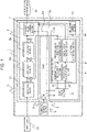
- Fig. 1 is a configuration example of a controller 11 on which a FPGA 1 according to a first implementation example is mounted.
- the FPGA 1 connects, to the outside, a CAM data storage section 12 including, for example, a flash ROM storing CRAM data defining logical circuit information.
- a CAM data storage section 12 including, for example, a flash ROM storing CRAM data defining logical circuit information.
- the CRAM data stored on the CAM data storage section 12 is downloaded to a CRAM 2 via a CRAM access interface circuit 5, a user-defined logical circuit is decided for the FPGA 1, and the FPGA 1 starts operation.
- the FPGA 1 includes: the CRAM 2 representing a region storing logical circuit information; a user logic section 3 that performs calculations for control of user logics; an error diagnosing section 4 for the user logics; a shutdown control section 10 for the user logics; and the CRAM access interface circuit 5.
- the user logic section 3 includes: duplicated user logic blocks (6a to 6c) for realizing a controller functionality; and a previous value retaining section 7 that retains output of the user logic block (6c) at the last stage in the user logic blocks in accordance with an instruction from the error diagnosing section 4.
- the user logic section 3 executes calculations at the user logic blocks (6a to 6c), retains calculation execution results at the previous value retaining section 7, and outputs output data 21.
- Each user logic block is duplicated, and calculation results of both user logic blocks are compared at a comparator. In a case that there is an inconsistency, an error occurrence notification 33 is given to a previous-value-retention instructing section of the error diagnosing section 4.
- the error diagnosing section 4 includes: a CRAM check section 8 that performs a CRAM cyclic check; and an error handling section 9 that gives an instruction for error handling in accordance with an assessment as to whether or not an error having occurred in the FPGA is caused by a soft error.
- the CRAM check section 8 reads out data from the CRAM 2 storing configuration information (logical circuit information) of the user logic section 3, and checks data validity.
- a scan interrupt signal 31 including scan region information e.g. in a case that there is an inconsistency in calculation results of the user logic block 2 (6b)
- a notification to that effect (an error occurrence notification) 33 arrives at the error handling section 9, and an interrupt scan instructing section of the error handling section 9 generates a scan interrupt signal 31 as scan region information representing an address of CRAM data stored on the CRAM 2 defining the configuration of the user logic block 2) is received from the error handling section 9, the CRAM check section 8 suspends a data validity check of the CRAM cyclic check that is being executed constantly, and checks the validity of the CRAM data in a region specified by the input scan region information.
- a validity check result 32 including an error correction possibility/impossibility result is notified to the error handling section 9.
- ECC Error Correction Code
- CRC Cycric Redundancy Code
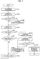
- FIG. 2 A flowchart of processes of the validity check of the CRAM data by the CRAM check section 8 is depicted in Fig. 2 .
- a read address of the CRAM data stored on the CRAM 2 whose data validity is to be checked is initialized (S101).
- the CRAM data is read out in accordance with the read address, an error check is performed by using ECC (S102), and it is checked whether there is an error (S103).
- error correction is performed (S104).
- the error correction in this procedure there are differences in performance such as capability of 1-bit correction or capability of 2-bit correction depending on ECC to be used. For example, in a case that the correction is performed on data having a 2-bit error by using ECC capable of 1-bit correction, the data is not corrected correctly, or it is recognized mistakenly that there are no errors, in some cases.
- a CRC check is performed by rereading the CRAM data (S105), and it is checked whether or not there is a CRC error (S106).
- the read address is updated (S109), and the procedure proceeds to a check (S102) of the next CRAM data.
- the read address is updated to a read address of the next CRAM at a time of the CRAM cyclic check.
- the read address is updated to a read address of the next CRAM in the scan region information. If checks of all read addresses in the scan region information have been ended, the read address is update to a read address of the CRAM cyclic check that has been suspended at a time point when the scan interrupt signal is received.
- a CRC check is performed by rereading the CRAM data from the CRAM 2 (S111), and it is checked whether or not there is a CRC error (S112).
- an error-correction-completion notification 32 is transmitted to the error handling section 9 (S108), and the procedure proceeds to a process of updating the read address at S109.
- the procedure returns to the read address initialization procedure S101, the CRAM data address of the region specified by the scan region information is set as a read address, and the operation of, and after the procedure S102 is performed. In the updating of the read address at the procedure S109, an address in the specified scan region is set.
- redundant bits for ECC and CRC are retained in a SRAM (not depicted) in the FPGA 1 in advance, both redundant bits are added when the CRAM data is downloaded from the CAM data storage section 12, and stored on the CRAM 2.
- redundant bits for ECC, and CRC may be added in advance to the CRAM data in the CAM data storage section 12.
- FIG. 3 A flowchart of operation by the error handling section 9 is depicted in Fig. 3 .
- the procedure waits until the error-correction-completion notification 32 or the error-correction-impossibility notification 32 is received from the CRAM check section 8 (S204).
- a shutdown instruction 36 is transmitted to the shutdown control section 10 (S208), and the procedure is ended.
- the shutdown control section 10 shuts down the FPGA 1.
- a user logic block to be reset is decided (S205), and a logical reset instruction 35 is transmitted (S206).
- a method of deciding a user logic block to be reset for example, there is a method in which a user logic block where there is an error, and user logic blocks following the block are treated as reset subjects.
- a previous-value-retention cancellation signal 34 is transmitted to the previous value retaining section 7 (S207), subsequently the procedure proceeds to S201, and the operation is continued.
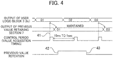
- the previous-value retention state of the previous value retaining section 7 is turned on 42. Thereafter, until the error handling section 9 transmits the previous-value-retention cancellation signal 34, and the previous-value retention state of the previous value retaining section 7 is turned off 43 after error correction of CRAM data stored on the CRAM 2 succeeds, the previous value retaining section 7 keeps the output values. That is, even if the value acquisition timing 41 of a control period signal has come while the previous-value retention state that had been turned on 42 has not been turned off 43, output values of the user logic block 3 are not received, and the previous value D1 is kept being output.
- the configuration of the present implementation example can enhance the availability.
- the functionalities of the FPGA 1 can be maintained, but if an error occurs in the user logic blocks (6a to 6c), it becomes not possible to perform detection, and correction.
- the error diagnosing section 4 is redundantized in order to enhance the error correction reliability of the error diagnosing section 4.
- An error monitoring section of an error diagnosing section that monitors inconsistencies between output of the redundantized error diagnosing sections may be provided, and the error monitoring section may output a shutdown control signal to the shutdown control section 10 at a time of occurrence an inconsistency between the output.
- diagnostic data is output for each step of operation of the CRAM check section 8 and the error handling section 9, and checks are performed outside.
- the FPGA 1 in the present implementation example it is possible to reduce the likelihood that the controller is shut down due to an error detected by an error check mechanism of user circuits such as redundancy, and it is possible to enhance the availability of the controller.
- Fig. 5 is a second implementation example. Portions that have counterparts in Fig. 1 are given the same reference signs, and because their configuration, and operation are the same, explanations thereof are omitted.
- the CRAM check is executed by giving priorities to the user logic blocks.
- a FPGA 14 in the present implementation example has, as a constituent element, an error diagnosing section 15 including: a check order deciding section 17 that decides a check order of the CRAM check; and a CRAM check section 16 that constantly executes the CRAM check in accordance with the check order decided at the check order deciding section 17.
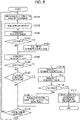
- Fig. 6 depicts a flow of operation by the CRAM check section 16. Portions that have counterparts in the flow of operation in Fig. 2 are gave the same step numbers, and because their operation is the same, explanations thereof are omitted.
- the CRAM check section 16 acquires region information to be checked from the check order deciding section 17 (S114).
- region information at least one or more CRAM address ranges included in a region are included.
- the CRAM check section 16 sets, as a read address, one of addresses in the CRAM address ranges in the acquired region information (S115), and executes the CRAM check operation (S102 to S113).
- Step S116 If checks of the entire CRAM data in the region have not been completed at Step S116, the procedure proceeds to S115, a read address is decided again (S115), and the CRAM check operation is repeated.
- Step S116 If checks of the entire CRAM data in the region have been completed at Step S116, the procedure proceeds to S114, the next check region information is acquired from the check order deciding section 17 (S114), a read address is set (S115), and the CRAM check operation is repeated.
- the check order deciding section 17 Upon receiving a region information request from the CRAM check section 16, the check order deciding section 17 generates region information by using a check count table, and a CRAM address range information table that are retained therein, and transmits the region information to the CRAM check section 16.
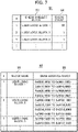
- Fig. 7 is configuration examples of a check count table 51, and a CRAM address range information table 52.
- the check count table 51 is a table representing correspondence between names (53) of check subject blocks, and check counts (54) of the blocks.
- the example in Fig. 7 depicts that the user logic block 1 is checked 20 times, the user logic block 3 is checked once, and the user logic block 2 is checked once, in this order.
- the CRAM address range information table 52 is a table representing correspondence between names (55) the blocks, and one or more address ranges (56) of the CRAM forming the blocks.
- the check order deciding section 17 Upon receiving a region information request from the CRAM check section 16, the check order deciding section 17 performs conversion into a CRAM address range 56 by using the CRAM address range information table 52 relevant to a check subject block decided by using the check count table 51, and transmits the CRAM address range 56 to the CRAM check section 16.
- CRAM check frequencies of user logic blocks in the FPGA 14 mounted on a controller 18 can be set freely.
- the CRAM check of a user logic block (6d in Fig. 5 ) for which an error check mechanism such as duplication cannot be provided, and which is less error-tolerant is performed frequently the CRAM check of user logic blocks (6b, and 6c in Fig. 5 ) for which an error check mechanism such as duplication is provided is performed less frequently, and so on, in one possible method.
- user logic blocks are divided into one that achieves a control functionality of a sequencer and the like, and a data processing functionality of calculation and the like, a CRAM of the user logic block that realizes the control functionality is checked frequently, and a CRAM of the user logic block that realizes the data processing functionality is checked less frequently, and so on.
Landscapes
- Engineering & Computer Science (AREA)
- Theoretical Computer Science (AREA)
- General Engineering & Computer Science (AREA)
- Physics & Mathematics (AREA)
- Quality & Reliability (AREA)
- General Physics & Mathematics (AREA)
- Mathematical Physics (AREA)
- Computer Security & Cryptography (AREA)
- Computer Hardware Design (AREA)
- Computing Systems (AREA)
- Detection And Correction Of Errors (AREA)
- Programmable Controllers (AREA)
- For Increasing The Reliability Of Semiconductor Memories (AREA)
Applications Claiming Priority (2)
| Application Number | Priority Date | Filing Date | Title |
|---|---|---|---|
| JP2020010493A JP7157773B2 (ja) | 2020-01-27 | 2020-01-27 | プログラマブルデバイス及びこれを用いた制御コントローラ |
| PCT/JP2020/031159 WO2021152887A1 (ja) | 2020-01-27 | 2020-08-18 | プログラマブルデバイス及びこれを用いた制御コントローラ |
Publications (2)
| Publication Number | Publication Date |
|---|---|
| EP4099105A1 true EP4099105A1 (de) | 2022-12-07 |
| EP4099105A4 EP4099105A4 (de) | 2024-02-28 |
Family
ID=77079834
Family Applications (1)
| Application Number | Title | Priority Date | Filing Date |
|---|---|---|---|
| EP20916427.6A Withdrawn EP4099105A4 (de) | 2020-01-27 | 2020-08-18 | Programmierbare vorrichtung und kontrollregler damit |
Country Status (4)
| Country | Link |
|---|---|
| US (1) | US11822425B2 (de) |
| EP (1) | EP4099105A4 (de) |
| JP (1) | JP7157773B2 (de) |
| WO (1) | WO2021152887A1 (de) |
Families Citing this family (1)
| Publication number | Priority date | Publication date | Assignee | Title |
|---|---|---|---|---|
| US20250278525A1 (en) * | 2024-03-04 | 2025-09-04 | Xilinx, Inc. | Cram validation using an external device |
Family Cites Families (14)
| Publication number | Priority date | Publication date | Assignee | Title |
|---|---|---|---|---|
| US7111224B1 (en) * | 2001-02-28 | 2006-09-19 | Xilinx, Inc. | FPGA configuration memory with built-in error correction mechanism |
| US20120011423A1 (en) * | 2010-07-10 | 2012-01-12 | Mehdi Entezari | Silent error detection in sram-based fpga devices |
| WO2012047735A2 (en) * | 2010-09-29 | 2012-04-12 | The Regents Of The University Of California | In-place resynthesis and remapping techniques for soft error mitigation in fpga |
| US8436646B1 (en) * | 2011-07-01 | 2013-05-07 | Altera Corporation | Reconfigurable logic block with user RAM |
| JP6326422B2 (ja) * | 2013-09-30 | 2018-05-16 | 株式会社日立製作所 | プログラマブルロジックデバイス、及び、論理集積ツール |
| JP6408482B2 (ja) | 2013-11-08 | 2018-10-17 | 株式会社日立製作所 | プログラマブルデバイス及びこれを用いた電子システム装置 |
| JP2015115727A (ja) * | 2013-12-11 | 2015-06-22 | 三菱電機株式会社 | プログラマブルロジックデバイス |
| JP6488541B2 (ja) | 2013-12-18 | 2019-03-27 | 富士通株式会社 | 論理回路及び論理回路の制御方法 |
| WO2016110968A1 (ja) * | 2015-01-07 | 2016-07-14 | 株式会社日立製作所 | プログラマブルデバイス及びそれを用いた制御装置、及びその障害対策方法 |
| JP2016167669A (ja) * | 2015-03-09 | 2016-09-15 | 富士通株式会社 | プログラマブル論理回路装置及びそのエラー検出方法 |
| WO2016207933A1 (ja) * | 2015-06-22 | 2016-12-29 | 株式会社日立製作所 | フィールドプログラマブルゲートアレイ |
| US9934841B1 (en) * | 2016-10-21 | 2018-04-03 | Altera Corporation | Systems and methods for refreshing data in memory circuits |
| US10248484B2 (en) * | 2017-02-21 | 2019-04-02 | Intel Corporation | Prioritized error-detection and scheduling |
| JP2018181206A (ja) * | 2017-04-20 | 2018-11-15 | 日本電気株式会社 | データ処理装置、データ処理方法およびプログラム |
-
2020
- 2020-01-27 JP JP2020010493A patent/JP7157773B2/ja active Active
- 2020-08-18 EP EP20916427.6A patent/EP4099105A4/de not_active Withdrawn
- 2020-08-18 US US17/795,025 patent/US11822425B2/en active Active
- 2020-08-18 WO PCT/JP2020/031159 patent/WO2021152887A1/ja not_active Ceased
Also Published As
| Publication number | Publication date |
|---|---|
| US20230082529A1 (en) | 2023-03-16 |
| JP2021117720A (ja) | 2021-08-10 |
| EP4099105A4 (de) | 2024-02-28 |
| WO2021152887A1 (ja) | 2021-08-05 |
| JP7157773B2 (ja) | 2022-10-20 |
| US11822425B2 (en) | 2023-11-21 |
Similar Documents
| Publication | Publication Date | Title |
|---|---|---|
| CN107534592B (zh) | 用于保护数据总线收发器的配置数据的方法、数据总线收发器和数据总线系统 | |
| US9535784B2 (en) | Self monitoring and self repairing ECC | |
| US10379946B2 (en) | Controller | |
| CN110716823A (zh) | 用于连续验证器件状态完整性的系统和方法 | |
| EP3968162B1 (de) | Abschwächung von einzelereignisstörungen durch containerisierung | |
| US11822425B2 (en) | Programmable device, and controller using the same | |
| JP2013175118A (ja) | 制御装置、及びそのメモリ故障検出方法、その自己診断方法 | |
| CN106716387B (zh) | 存储器诊断电路 | |
| US10191793B2 (en) | Microprocessor device with reset timer | |
| US11831337B2 (en) | Semiconductor device and error detection methods | |
| US10514970B2 (en) | Method of ensuring operation of calculator | |
| JP4941954B2 (ja) | データエラー検出装置およびデータエラー検出方法 | |
| JP7379932B2 (ja) | 制御装置、ユーザプログラムの実行制御方法、およびシステムプログラム | |
| EP3882774A1 (de) | Datenverarbeitungsvorrichtung und datenverarbeitungsverfahren | |
| US20230055743A1 (en) | Information processing device, control method, and non-transitory computer readable medium | |
| US12524304B2 (en) | Electronic device, electronic system, method for operating an electronic device, and method for operating an electronic system | |
| US8074120B2 (en) | Method for recognizing a power failure in a data memory and recovering the data memory | |
| US20250077339A1 (en) | Data processing system and data processing method | |
| WO2024190403A1 (ja) | 半導体装置、およびそれを備えた情報処理装置 | |
| Beningo | A review of watchdog architectures and their application to Cubesats | |
| CN105830162B (zh) | 用于识别至少一个存储器元件中的错误数据的方法和装置 | |
| JP2015201814A (ja) | プログラマブルゲートアレイ及び電子装置 |
Legal Events
| Date | Code | Title | Description |
|---|---|---|---|
| STAA | Information on the status of an ep patent application or granted ep patent |
Free format text: STATUS: THE INTERNATIONAL PUBLICATION HAS BEEN MADE |
|
| PUAI | Public reference made under article 153(3) epc to a published international application that has entered the european phase |
Free format text: ORIGINAL CODE: 0009012 |
|
| STAA | Information on the status of an ep patent application or granted ep patent |
Free format text: STATUS: REQUEST FOR EXAMINATION WAS MADE |
|
| 17P | Request for examination filed |
Effective date: 20220620 |
|
| AK | Designated contracting states |
Kind code of ref document: A1 Designated state(s): AL AT BE BG CH CY CZ DE DK EE ES FI FR GB GR HR HU IE IS IT LI LT LU LV MC MK MT NL NO PL PT RO RS SE SI SK SM TR |
|
| DAV | Request for validation of the european patent (deleted) | ||
| DAX | Request for extension of the european patent (deleted) | ||
| A4 | Supplementary search report drawn up and despatched |
Effective date: 20240131 |
|
| RIC1 | Information provided on ipc code assigned before grant |
Ipc: H03K 19/17764 20200101ALI20240125BHEP Ipc: H03K 19/1776 20200101ALI20240125BHEP Ipc: G05B 19/042 20060101AFI20240125BHEP |
|
| STAA | Information on the status of an ep patent application or granted ep patent |
Free format text: STATUS: THE APPLICATION IS DEEMED TO BE WITHDRAWN |
|
| 18D | Application deemed to be withdrawn |
Effective date: 20240821 |