EP4099403A1 - Solarzelle und frontelektrode dafür sowie herstellungsverfahren - Google Patents
Solarzelle und frontelektrode dafür sowie herstellungsverfahren Download PDFInfo
- Publication number
- EP4099403A1 EP4099403A1 EP21914089.4A EP21914089A EP4099403A1 EP 4099403 A1 EP4099403 A1 EP 4099403A1 EP 21914089 A EP21914089 A EP 21914089A EP 4099403 A1 EP4099403 A1 EP 4099403A1
- Authority
- EP
- European Patent Office
- Prior art keywords
- fine
- busbar
- busbars
- solar cell
- front electrode
- Prior art date
- Legal status (The legal status is an assumption and is not a legal conclusion. Google has not performed a legal analysis and makes no representation as to the accuracy of the status listed.)
- Pending
Links
Images


Classifications
-
- H—ELECTRICITY
- H10—SEMICONDUCTOR DEVICES; ELECTRIC SOLID-STATE DEVICES NOT OTHERWISE PROVIDED FOR
- H10F—INORGANIC SEMICONDUCTOR DEVICES SENSITIVE TO INFRARED RADIATION, LIGHT, ELECTROMAGNETIC RADIATION OF SHORTER WAVELENGTH OR CORPUSCULAR RADIATION
- H10F77/00—Constructional details of devices covered by this subclass
- H10F77/20—Electrodes
- H10F77/206—Electrodes for devices having potential barriers
- H10F77/211—Electrodes for devices having potential barriers for photovoltaic cells
- H10F77/215—Geometries of grid contacts
-
- H—ELECTRICITY
- H10—SEMICONDUCTOR DEVICES; ELECTRIC SOLID-STATE DEVICES NOT OTHERWISE PROVIDED FOR
- H10F—INORGANIC SEMICONDUCTOR DEVICES SENSITIVE TO INFRARED RADIATION, LIGHT, ELECTROMAGNETIC RADIATION OF SHORTER WAVELENGTH OR CORPUSCULAR RADIATION
- H10F77/00—Constructional details of devices covered by this subclass
- H10F77/93—Interconnections
- H10F77/933—Interconnections for devices having potential barriers
- H10F77/935—Interconnections for devices having potential barriers for photovoltaic devices or modules
- H10F77/937—Busbar structures for modules
-
- H—ELECTRICITY
- H10—SEMICONDUCTOR DEVICES; ELECTRIC SOLID-STATE DEVICES NOT OTHERWISE PROVIDED FOR
- H10F—INORGANIC SEMICONDUCTOR DEVICES SENSITIVE TO INFRARED RADIATION, LIGHT, ELECTROMAGNETIC RADIATION OF SHORTER WAVELENGTH OR CORPUSCULAR RADIATION
- H10F71/00—Manufacture or treatment of devices covered by this subclass
- H10F71/121—The active layers comprising only Group IV materials
-
- H—ELECTRICITY
- H10—SEMICONDUCTOR DEVICES; ELECTRIC SOLID-STATE DEVICES NOT OTHERWISE PROVIDED FOR
- H10F—INORGANIC SEMICONDUCTOR DEVICES SENSITIVE TO INFRARED RADIATION, LIGHT, ELECTROMAGNETIC RADIATION OF SHORTER WAVELENGTH OR CORPUSCULAR RADIATION
- H10F77/00—Constructional details of devices covered by this subclass
- H10F77/20—Electrodes
- H10F77/206—Electrodes for devices having potential barriers
- H10F77/211—Electrodes for devices having potential barriers for photovoltaic cells
-
- H—ELECTRICITY
- H10—SEMICONDUCTOR DEVICES; ELECTRIC SOLID-STATE DEVICES NOT OTHERWISE PROVIDED FOR
- H10F—INORGANIC SEMICONDUCTOR DEVICES SENSITIVE TO INFRARED RADIATION, LIGHT, ELECTROMAGNETIC RADIATION OF SHORTER WAVELENGTH OR CORPUSCULAR RADIATION
- H10F77/00—Constructional details of devices covered by this subclass
- H10F77/30—Coatings
- H10F77/306—Coatings for devices having potential barriers
- H10F77/311—Coatings for devices having potential barriers for photovoltaic cells
- H10F77/315—Coatings for devices having potential barriers for photovoltaic cells the coatings being antireflective or having enhancing optical properties
-
- H—ELECTRICITY
- H10—SEMICONDUCTOR DEVICES; ELECTRIC SOLID-STATE DEVICES NOT OTHERWISE PROVIDED FOR
- H10F—INORGANIC SEMICONDUCTOR DEVICES SENSITIVE TO INFRARED RADIATION, LIGHT, ELECTROMAGNETIC RADIATION OF SHORTER WAVELENGTH OR CORPUSCULAR RADIATION
- H10F10/00—Individual photovoltaic cells, e.g. solar cells
- H10F10/10—Individual photovoltaic cells, e.g. solar cells having potential barriers
- H10F10/14—Photovoltaic cells having only PN homojunction potential barriers
-
- H—ELECTRICITY
- H10—SEMICONDUCTOR DEVICES; ELECTRIC SOLID-STATE DEVICES NOT OTHERWISE PROVIDED FOR
- H10F—INORGANIC SEMICONDUCTOR DEVICES SENSITIVE TO INFRARED RADIATION, LIGHT, ELECTROMAGNETIC RADIATION OF SHORTER WAVELENGTH OR CORPUSCULAR RADIATION
- H10F77/00—Constructional details of devices covered by this subclass
- H10F77/93—Interconnections
- H10F77/933—Interconnections for devices having potential barriers
- H10F77/935—Interconnections for devices having potential barriers for photovoltaic devices or modules
-
- Y—GENERAL TAGGING OF NEW TECHNOLOGICAL DEVELOPMENTS; GENERAL TAGGING OF CROSS-SECTIONAL TECHNOLOGIES SPANNING OVER SEVERAL SECTIONS OF THE IPC; TECHNICAL SUBJECTS COVERED BY FORMER USPC CROSS-REFERENCE ART COLLECTIONS [XRACs] AND DIGESTS
- Y02—TECHNOLOGIES OR APPLICATIONS FOR MITIGATION OR ADAPTATION AGAINST CLIMATE CHANGE
- Y02E—REDUCTION OF GREENHOUSE GAS [GHG] EMISSIONS, RELATED TO ENERGY GENERATION, TRANSMISSION OR DISTRIBUTION
- Y02E10/00—Energy generation through renewable energy sources
- Y02E10/50—Photovoltaic [PV] energy
-
- Y—GENERAL TAGGING OF NEW TECHNOLOGICAL DEVELOPMENTS; GENERAL TAGGING OF CROSS-SECTIONAL TECHNOLOGIES SPANNING OVER SEVERAL SECTIONS OF THE IPC; TECHNICAL SUBJECTS COVERED BY FORMER USPC CROSS-REFERENCE ART COLLECTIONS [XRACs] AND DIGESTS
- Y02—TECHNOLOGIES OR APPLICATIONS FOR MITIGATION OR ADAPTATION AGAINST CLIMATE CHANGE
- Y02P—CLIMATE CHANGE MITIGATION TECHNOLOGIES IN THE PRODUCTION OR PROCESSING OF GOODS
- Y02P70/00—Climate change mitigation technologies in the production process for final industrial or consumer products
- Y02P70/50—Manufacturing or production processes characterised by the final manufactured product
Definitions
- This disclosure relates to the solar cell technology, and in particular, to a solar cell and a front electrode thereof, and a manufacturing method.
- a crystalline silicon solar cell is a device that uses the photovoltaic effect of PN junction to convert light energy into electrical energy.
- a passivated emitter and rear contact (PERC) cell has been gradually developed to a mainstream high-efficiency solar cell product and technology in the market. How to further improve the conversion efficiency of the PERC cell, narrow the conversion efficiency difference with other high-efficiency cells such as a heterojunction technology (HJT) cell, a tunnel oxide passive contact (TOPCon) cell, and maintain the comprehensive cost-performance advantage of the PERC cell is an issue that PERC+ technology continues to face in future.
- HJT heterojunction technology
- TOPCon tunnel oxide passive contact
- the PERC cell module has received increasing attention from researchers and customers in reliability and durability performance.
- Various attenuation phenomena such as PID effect, LID, LETID, backplane's aging and cracking, EVA's yellowing and other issues can affect the lifetime of photovoltaic modules.
- the warranty period of photovoltaic modules has been extended from 5 years to at least 25 years.
- the International Renewable Energy Laboratory IRL has conducted indoor accelerated aging tests on crystalline silicon modules (including ISC61215 and UL1703 standards) to assess the factory quality of the modules and to approximate the long-term reliability of the modules during their warranty period under outdoor operating conditions. From a long-term perspective, high-efficiency and high-reliability cells and modules are still the main direction for the future development of the photovoltaic industry.
- a Multi-Busbar (MBB) cell (with nine or more busbars), on the one hand, can significantly improve cell efficiency, and on the other hand, can effectively reduce consumption of silver paste, thus the MBB technology is gradually increasing its market share and further developing to busbar-free technology.
- MBB Multi-Busbar
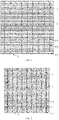
- a design of a MBB pattern is generally focus on solder joints 3-1, fine busbars 3-2 and edge harpoon-shaped fine busbars 3-3 in a busbar area.
- a molten tin of a solder strip and silver paste of the busbar form a silver-tin alloy at high temperature to achieve metal connection.
- the tension is mainly provided by the welding between the solder joint and the solder strip on the busbar.
- the fine busbar may have an increased resistance after soldering because of less silver paste, which affects the current collection in some areas.
- the solder strip may be misaligned to a certain extent during the soldering process, so that the solder strip in the fine busbar area may be soldered with a finger perpendicular to the busbar, which may easily cause the finger to be broken or partial broken in the soldering area, resulting that the electroluminescence (EL) may indicate a broken line after the soldering process.
- the resistance in this area may become larger due to smaller adhesion or fracture problem, eventually leading to a continuous decline in power generation, affecting product quality and reliability.
- a patent application No. CN201820897922.0 provides a front electrode structure of a multi-busbar solar cell and a solar cell having the same.
- the finger includes a straight section and a deformation section, the deformation section is disposed at an intersection area of the finger and the busbar, a width of the deformation section gradually widens from an end of the straight section to the busbar, a height of the deformation section is greater than a height of the straight section, and a total width of the deformation section is greater than or equal to a width of a solder pad.
- a deformation area is designed at a connection area of a fine busbar and the finger to increase the total amount of silver paste in the area, thereby addressing the problem of the finger breakage in the soldering process of the multiple busbar solar cell to a certain extent. Nevertheless, the effect is not very satisfactory, and further improvement is still needed.
- a Chinese patent application No. CN201711417592.7 discloses a new type of multi-busbar solar cell and a photovoltaic module using the multi-busbar solar cell, the busbar is designed as a double-line and flat ellipse-type composite shape structure, an end point of each small flat ellipse is taken as a welding reinforcement point to improve its reliability.
- the double-line composite busbar when one end of the busbar has defects such as aging and broken, the other end of the busbar can still collect current normally, which would not cause reduction of the overall power generation substantially.
- the use of the busbar structure in this application is beneficial to avoid the soldering effect of the fine busbar and the solder strip to a certain extent, but may reduce the current collection effect of the fine busbar and the soldering connection.
- a purpose of the present disclosure is to solve the problem that the quality and reliability of an existing PERC solar cell need to be further improved, and to provide a high-efficiency and high-reliability PERC solar cell, a front electrode thereof and a manufacturing method.
- the technical solutions of the present disclosure can effectively improve the quality and reliability of the solar cell while improving the conversion efficiency of the solar cell.
- a busbar of the front electrode includes fine busbars and solder joints distributed on the fine busbars at intervals.
- Each fine busbar between adjacent solder joints includes a straight fine busbar connecting the two solder joints, and side fine busbars located on both sides of the straight fine busbar respectively.
- a width of the straight fine busbars and a width of the side fine busbars are both 0.06 ⁇ 0.04mm.
- the side fine busbars are disposed divergently with respect to each solder joint, and a spacing W2 between the two side fine busbars is greater than a width W1 of the solder joint.
- each side fine busbar between adjacent solder joints is a straight line or a curve line. More preferably, each side fine busbar between adjacent solder joints is a straight line parallel to the straight fine busbar, and two ends of each side fine busbar are connected to the solder joints respectively by a transition connection line.
- each straight fine busbar is respectively connected to a central region of the two solder joints, and the side fine busbars on both sides of each straight fine busbar are symmetrically distributed with respect to the corresponding straight fine busbar.
- fingers of the front electrode are printed by a knotless screen.
- the two ends of the fine busbars are provided with edge harpoon fine busbars, and the edge harpoon fine busbars are designed with an S-type curve line.
- the fingers are vertically distributed with the busbars, and a spacing between adjacent fingers ranges from 1.00mm to 1.32mm, and a width of the fingers ranges from 10 ⁇ m to 26 ⁇ m.
- the present disclosure further provides a method for manufacturing the front electrode of the solar cell, including: forming the busbars and the fingers by using a step-by-step printing process.
- solder joints and the fine busbars are synchronously printed during a process of printing the busbar area; and the fingers and the edge harpoon-shaped fine busbars are synchronously printed during a process of printing the finger area.
- the fingers area is printed by a knotless screen.
- the present disclosure further provides a solar cell includes the front electrode as described.
- the design of the structure of the busbars is optimized, the fine busbar between adjacent solder joints is designed as a composite structure including a straight fine busbar and side fine busbars on both sides.
- the fingers can be prevented from breaking at the soldering area of the busbars. That is, the influence on the solar cell and the solar cell module caused by the soldering connections between the fine busbars and the solder scrips in an existing front electrode can be overcome, thereby improving the quality and reliability of the solar cell and the solar cell module.
- the fingers are printed by using the knotless screen, which can eliminate the knots in the warp and weft in the steel wire mesh on the fingers, and effectively improve the ink permeability of silver paste of screen printing and the fluctuation issue of 3D topography of grid lines.
- the present disclosure can effectively solve the problem that missing print may be easily formed at the knot positions of the busbar area when using the knotless screen printing technology, which further ensures the quality and reliability of the solar cell products.
- the edge harpoon-shaped fine busbar at each of the both ends of the fine busbar is designed as a S-type curve line, which can effectively reduce the knots formed by the longitudinal and transverse wires of the wire mesh in the harpoon-shaped busbar area by more than 80%, thereby further improving the quality and reliability of the solar cell products.
- the photoelectric conversion efficiency of the PERC solar cell can be improved by more than 0.1%, and the consumption of front silver paste can be reduced by 3-10mg. Meanwhile, the quality and reliability of the solar cell and the solar cell module can also be effectively improved.
- the fingers are printed by using the knotless screen technology and the step-by-step printing process, which eliminates the problem of poor ink permeability of the front silver paste and the fluctuation issue of the grid lines caused by knots of the steel mesh.
- This can break the limitation that the paste of fingers has a high requirement of tensile force on the busbar area, thereby improving the metallization performance of the fingers area, and reducing the width of the fingers to 10-26 ⁇ m, and reducing the shading area and the consumption of the silver paste.
- the spacing between adjacent fingers can be effectively reduced to 1.00mm-1.32mm, which matches the diffusion sheet resistance of 155-250 ⁇ / ⁇ , and improves the conversion efficiency of the solar cell.
- the impact caused by the soldering of the busbar area of the front electrode and the knotless screen process for printing the fingers can be effectively overcome.
- the photoelectric conversion efficiency of PERC solar cells can be effectively promoted, and the quality and reliability of the solar cells improved as well.
- 1 front electrode
- 2 finger
- 3 busbar
- 3-1 solder joint
- 3-2 fine busbar
- 3-2-1 side fine busbar
- 3-2-2 straight fine busbar
- 3-3 edge harpoon-shaped fine busbar
- 4 transverse wire of wire mesh
- 5 longitudinal wire of wire mesh
- 6 knot of longitudinal and transverse wires
- 7 finger printing area
- 8 transverse wire cut by laser in the finger printing area
- 9-1 straight harpoon-shaped busbar printing area
- 9-2 S-type harpoon-shaped busbar printing area
- 10 silicon substrate
- 11 front emitter
- 11-1 lightly doped region
- 11-2 heavily doped region
- 12 front passivation and anti-reflection layer
- 13 front oxide layer
- 14 back passivation layer
- 15 back finger electrode
- 16 laser doping area of fingers
- 16-1 laser spot.
- the present disclosure provides an optimized design of the busbar structure of the front electrode, that is, the structure of the busbar is designed as a composite structure which includes straight fine busbars 3-2-2 connected between adjacent solder joints and side fine busbars 3-2-1 located on both sides of the straight fine busbars 3-2-2 respectively.
- the busbar of the composite structure can effectively guarantee the current collection effect of the connection between the fine busbars and the solder scrips, and prevent the fingers from breaking at the soldering area of the busbars, that is, overcome the influence of the soldering of the fine busbar and the solder scrips in the existing front electrode on a solar cell and a solar cell module, and improve the quality and reliability of the solar cell and the solar cell module.
- the side fine busbars 3-2-1 are disposed divergently with respect to the solder joint 3-1, and a spacing W2 between the two side fine busbars 3-2-1 is greater than a width W1 of the solder joint 3-1, and each side fine busbar 3-2-1 can be a straight line or a curve line, preferably a straight line.
- the knotless screen mainly adopts a laser removal process of filaments, which has the advantages of high pattern making efficiency and high yield rate, and further does not need to change a pattern of the front electrode, etc., and gradually becomes mainstream.
- the fingers are printed by using a knotless screen, which can eliminate knots in the warp and weft of the wire mesh on the fingers and effectively improve the ink permeability of the paste of the screen printing and fluctuation of a 3D shape of the grid lines.
- the busbar 3 includes fine busbars 3-2 and solder joints 3-1 distributed on the fine busbars 3-2 at intervals.
- Each fine busbar 3-2 between two adjacent solder joints 3-1 includes a straight fine busbar 3-2-2 connecting the two adjacent solder joints 3-1, and side fine busbars 3-2-1 located on both sides of the straight fine busbar 3-2-2 respectively.
- the structure of the front electrode of the solar cell in this embodiment is basically the same as that in the first example, specifically, in this embodiment, a width of the straight fine busbar 3-2-2 and a width of the side fine busbar 3-2-1 are both 0.06 ⁇ 0.04mm.
- the side fine busbars 3-2-1 are disposed divergently with respect to the solder joints 3-1, and a spacing W2 between the two side fine busbars 3-2-1 is greater than a width of the solder joint 3-1, and each side fine busbar 3-2-1 between adjacent solder joints 3-1 can be a straight line or a curve line.
- each side fine busbar 3-2-1 between adjacent solder joints 3-1 is a curve line.
- each side fine busbar 3-2-1 between adjacent solder joints 3-1 is a straight line, as shown in FIG. 4 and FIG. 5 .
- the side fine busbars 3-2-1 are straight lines parallel to the straight fine busbar 3-2-2, it is better to configure the two ends of each side fine busbar 3-2-1 to be connected to the solder joint 3-1 respectively through a transition connection line.
- each straight fine busbar 3-2-2 are respectively connected to central regions of the two solder joints 3-1, and the two side fine busbars 3-2-1 are symmetrically distributed with respect to the straight fine busbar 3-2-2, that is, the straight fine busbar 3-2-2 between different solder joints 3-1 are in a common line.
- the structure of the front electrode of the solar cell in this embodiment is basically the same as that in the fourth example.
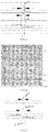
- the difference mainly lies in that, in this example, the fingers 2 are printed by using the knotless screen technology, and two ends of the fine busbars 3-2 are provided with edge harpoon-shaped fine busbars 3-3, and the edge harpoon-shaped fine busbar 3-3 is designed as an S-type curve line. As shown in FIG. 7 and FIG.
- the comparison between a straight harpoon-shaped busbar printing area 9-1 and a S-type harpoon-shaped busbar printing area 9-2 shows that the use of S-type design can effectively reduce the knots formed by the longitudinal and transverse wires of the wire mesh in the harpoon-shaped busbar area by more than 80%, which is beneficial to further improve the quality and reliability of the solar cell products.
- the busbars 3 and the fingers 2 are prepared by using a step-by-step printing process. Specifically, the solder joints 3-1 and the fine busbars 3-2 are simultaneously printed during the printing of the busbar area, and the fingers 2 and the edge harpoon-shaped fine busbars 3-3 are simultaneously printed during the printing of the fingers area.
- the printing of the fingers area is performed by using the knotless screen, a spacing between adjacent fingers 2 ranges from 1.00mm to 1.32mm, and a width of the finger 2 ranges from 10 ⁇ m to 26 ⁇ m.
- a high-efficiency and high-reliability PERC solar cell of the present embodiment includes back finger electrodes 15, a back passivation layer 14, a silicon substrate 10, a front emitter 11, and a front passivation and anti-reflection layer 12.
- the front electrode 1 is located on a front surface of the front passivation and anti-reflection layer 12, and forms ohmic contact with the front emitter 11.
- the structure of the front electrode 1 is the same as that of the embodiment 5.
- a method for manufacturing the solar cell of this embodiment includes the following steps.
- a texturing treatment is performed with alkali on a P-type monocrystalline silicon substrate 10 to form a textured surface structure on both a front surface and a back surface.
- the texturized silicon substrate is reacted with phosphorus oxychloride at a high temperature, so that the front surface of the silicon substrate diffuses to form a PN emitter junction (i.e., the front emitter 11).
- a sheet resistance of a thin layer of the front surface after diffusion is between 160 ⁇ / ⁇ .
- the diffused phospho silicate glass serves as a phosphorus source
- a laser doping process is performed on a metallization area located on the front surface of the diffused silicon substrate and corresponding to gate lines of the front electrode, to form a heavily doped region 11-2, thus the structure of the selective emitter (the heavily doped region 11-2 and the lightly doped region 11-1) is formed on the front surface of the silicon substrate.
- the sheet resistance of the heavily doped region is between 60 ⁇ / ⁇ . As shown in FIG.
- the laser SE doping is performed on the finger area of the pattern of the front electrode, as compared to the conventional laser pattern , the laser doping in the busbar area is eliminated, that is, the laser doping is performed only on a finger area 16, which increases the area of the lightly doped region, reduces surface recombination caused by heavy doping and laser process in this area, improves the short-wave effect, and is beneficial to further improve the conversion efficiency of the solar cell. As shown in FIG.
- a laser SE spot is square or rectangular with a width of 90 ⁇ m to 110 ⁇ m, and a spacing between laser spots 16-1 varies between 0 ⁇ m to 10 ⁇ m.
- the silicon substrate is oxidized by oxygen after the laser SE process.
- a hydrofluoric (HF) is used to remove the PSG from the back surface and surrounding area of the silicon substrate after thermal oxidation.
- Step 6 of alkali polishing the back surface and edges of the silicon substrate are polished after the PSG removing process, and the PSG on the front surface of the silicon substrate is removed.
- Step 7 of oxidation annealing oxidation and annealing treatments are performed on the alkali polished silicon substrate to form the front oxide layer 13.
- a passivation film is formed on the back surface of the annealed silicon substrate to form a back passivation layer 14.
- a front passivation and anti-reflection layer 12 is formed on the front surface of the silicon substrate.
- Step 10 of laser drilling is performed on the back surface of the silicon substrate having the passivation film.
- the back electrodes are formed on the silicon substrate by screen printing after the laser drilling is performed on the front and back surfaces.
- back finger electrodes 15 are formed on the silicon substrate having printed back electrodes, by screen printing.
- front silver paste is used to perform screen printing on the silicon substrate, which includes printed back aluminum grid lines, to form the busbars of the front electrode.
- the front silver paste has a high solid content, a high solderability, and would not burn through silicon nitride (e.g., a solid content is 80-95%, tin area is more than 80%, an average value of tensile force is more than 1.0N, in this embodiment, polymerization M3M-FB07-6 is used).
- the busbar pattern is configured in a manner of using the solder joints of the busbars and the fine busbars (as shown in FIG. 9 ).
- the busbar adopts a multi-busbar structure which includes nine or more busbars, a width of each fine busbar is 0.05mm.
- the fine busbar can be designed with a bamboo gradient structure, and a gradient specification is 0.03mm to 0.1mm.
- knotless front silver paste is used to perform screen print on the silicon substrate, which includes printed front busbars of the front electrode, by using the knotless screen, to form the fingers of the front electrode.
- the front silver paste has a good high aspect ratio, and would burn through the silicon nitride (e.g., a high aspect ratio greater than 35%, in this embodiment, polymerization CSP-M3D-S6009V229 is used). Referring to FIG.
- a process e.g., a laser removal of filaments is performed to remove the wires parallel to the fingers in the printing area of fingers 7 (transverse wires 8 to be removed by laser in the printing area of fingers), thus eliminating the originally existed knots (i.e., the longitudinal and transverse wire knots 6) formed by the longitudinal wires 5 of the wire mesh and the transverse wires 4 of the wire mesh in the finger area.
- a pattern with fingers corresponding to the busbar pattern and the harpoon-shaped fine busbars (as shown in FIG. 10 ) is used.
- a spacing between adjacent fingers is 1.22mm, and the fingers are parallel and evenly spaced.
- a width of the finger is designed to be 22 ⁇ m, and the harpoon-shaped fine busbars (as shown in FIG. 7 ) are designed to be S-type curve lines.
- the silicon substrate printed with the front electrode is co-sintered, and a peak sintering temperature can be selected between 720°C to 800°C as needed, in this embodiment, the temperature is 750°C.
- Step 16 of electrical injection and preparing finished product the electrical injection process is performed on the sintered solar cells, after that, the solar cells are tested, sorted and packed into storage.
- a solar cell of this embodiment has a same structure as the example 6.
- the spacing between adjacent fingers 2 can be reduced to 1.13mm, the width of the finger 2 can be reduced to 20 ⁇ m, and the sintering temperature is 750°C.
- a solar cell of this embodiment has a same structure as the example 6.
- the spacing between adjacent fingers 2 can be reduced to 1.32mm, the width of the finger 2 can be reduced to 24 ⁇ m, and the sintering temperature is 760°C.
- a solar cell of this embodiment has a same structure as the example 6.
- the spacing between adjacent fingers 2 can be reduced to 1.00mm, the width of the finger 2 can be reduced to 10 ⁇ m, and the sintering temperature is 755°C.
- the photoelectric conversion efficiency of the PERC solar cell can be improved by more than 0.1%, and the consumption of front silver paste can be reduced by 3-10mg.
- This can break the limitation that the paste of the fingers has a high requirement of tensile force on the busbar area, and the paste of the busbar area and the paste of the finger area can be selected separately as needed, thereby improving the metallization performance of the finger area.
- the width of the finger can be reduced to 10 ⁇ m-26 ⁇ m, and the spacing between adjacent fingers can be effectively reduced to 1.00mm -1.32mm.
Landscapes
- Photovoltaic Devices (AREA)
- Life Sciences & Earth Sciences (AREA)
- Sustainable Development (AREA)
- Engineering & Computer Science (AREA)
- Sustainable Energy (AREA)
Applications Claiming Priority (2)
| Application Number | Priority Date | Filing Date | Title |
|---|---|---|---|
| CN202011621762.5A CN112635586A (zh) | 2020-12-30 | 2020-12-30 | 一种高效高可靠性perc太阳能电池及其正面电极和制作方法 |
| PCT/CN2021/140577 WO2022143352A1 (zh) | 2020-12-30 | 2021-12-22 | 太阳能电池及其正面电极和制作方法 |
Publications (2)
| Publication Number | Publication Date |
|---|---|
| EP4099403A1 true EP4099403A1 (de) | 2022-12-07 |
| EP4099403A4 EP4099403A4 (de) | 2024-03-13 |
Family
ID=75287359
Family Applications (1)
| Application Number | Title | Priority Date | Filing Date |
|---|---|---|---|
| EP21914089.4A Pending EP4099403A4 (de) | 2020-12-30 | 2021-12-22 | Solarzelle und frontelektrode dafür sowie herstellungsverfahren |
Country Status (5)
| Country | Link |
|---|---|
| US (1) | US20230343878A1 (de) |
| EP (1) | EP4099403A4 (de) |
| CN (1) | CN112635586A (de) |
| AU (1) | AU2021414045A1 (de) |
| WO (1) | WO2022143352A1 (de) |
Cited By (1)
| Publication number | Priority date | Publication date | Assignee | Title |
|---|---|---|---|---|
| GB2612449A (en) * | 2021-10-29 | 2023-05-03 | Jinko Solar Co Ltd | Electrode structure, solar cell, and photovoltaic module |
Families Citing this family (16)
| Publication number | Priority date | Publication date | Assignee | Title |
|---|---|---|---|---|
| CN112635586A (zh) * | 2020-12-30 | 2021-04-09 | 通威太阳能(成都)有限公司 | 一种高效高可靠性perc太阳能电池及其正面电极和制作方法 |
| CN113421947A (zh) * | 2021-06-21 | 2021-09-21 | 苏州潞能能源科技有限公司 | 双面太阳能电池制作工艺 |
| CN117936599B (zh) | 2021-08-27 | 2025-11-04 | 晶科能源股份有限公司 | 一种光伏电池及光伏组件 |
| CN113903818A (zh) * | 2021-11-05 | 2022-01-07 | 通威太阳能(成都)有限公司 | 一种perc电池的se激光掺杂图形和perc电池制备方法 |
| WO2023123278A1 (zh) | 2021-12-30 | 2023-07-06 | 深圳市元征科技股份有限公司 | 车辆诊断方法、诊断连接器以及诊断设备 |
| CN114709276A (zh) * | 2022-03-31 | 2022-07-05 | 上饶捷泰新能源科技有限公司 | 分步印刷太阳能电池的方法及太阳能电池 |
| CN114695574A (zh) * | 2022-04-27 | 2022-07-01 | 浙江爱康光电科技有限公司 | 一种无主栅的异质结电池片 |
| CN218215317U (zh) * | 2022-08-03 | 2023-01-03 | 隆基绿能科技股份有限公司 | 一种太阳能电池和太阳能组件 |
| US12080819B2 (en) * | 2022-10-24 | 2024-09-03 | Zhejiang Jinko Solar Co., Ltd. | Solar cell and photovoltaic module |
| CN115763586A (zh) * | 2022-12-29 | 2023-03-07 | 江苏润阳世纪光伏科技有限公司 | 一种用于TOP-Con电池片主副栅搭接电阻测量的网板及方法 |
| CN116031314A (zh) | 2023-02-14 | 2023-04-28 | 浙江晶科能源有限公司 | 光伏电池及光伏组件 |
| CN117199152B (zh) * | 2023-09-11 | 2024-06-04 | 淮安捷泰新能源科技有限公司 | 一种太阳能电池及其制备方法 |
| CN117238985A (zh) | 2023-11-16 | 2023-12-15 | 浙江晶科能源有限公司 | 太阳能电池及光伏组件 |
| CN117712232B (zh) * | 2024-02-05 | 2024-05-07 | 晶科能源(海宁)有限公司 | 太阳能电池制备方法、太阳能电池及其光伏组件 |
| CN118073469B (zh) * | 2024-02-18 | 2025-06-03 | 天合光能股份有限公司 | 太阳能电池及其制备方法和光伏组件 |
| CN120936132B (zh) * | 2025-10-13 | 2026-03-31 | 晶科能源(海宁)有限公司 | 太阳能电池及其制备方法 |
Family Cites Families (21)
| Publication number | Priority date | Publication date | Assignee | Title |
|---|---|---|---|---|
| JP5025135B2 (ja) * | 2006-01-24 | 2012-09-12 | 三洋電機株式会社 | 光起電力モジュール |
| JP4294048B2 (ja) * | 2006-11-29 | 2009-07-08 | 三洋電機株式会社 | 太陽電池モジュール |
| EP2278623A2 (de) * | 2007-12-11 | 2011-01-26 | Evergreen Solar, Inc. | Photovoltaikpanel und -zelle mit feinen Fingern und Herstellungsverfahren dafür |
| WO2013039158A1 (ja) * | 2011-09-13 | 2013-03-21 | 京セラ株式会社 | 太陽電池モジュール |
| US10383207B2 (en) * | 2011-10-31 | 2019-08-13 | Cellink Corporation | Interdigitated foil interconnect for rear-contact solar cells |
| DE102014118332A1 (de) * | 2014-12-10 | 2016-06-16 | Solarworld Innovations Gmbh | Photovoltaikmodul |
| WO2016131222A1 (zh) * | 2015-02-16 | 2016-08-25 | 保定市易通光伏科技有限公司 | 光伏组件及其制造方法 |
| CN105529373B (zh) * | 2016-01-28 | 2018-01-16 | 黄河水电光伏产业技术有限公司 | 一种晶硅太阳能电池的正面电极 |
| CN206040654U (zh) * | 2016-08-31 | 2017-03-22 | 连云港神舟新能源有限公司 | 一种多主栅双面太阳电池组件 |
| CN106229356A (zh) * | 2016-08-31 | 2016-12-14 | 连云港神舟新能源有限公司 | 一种多主栅双面太阳电池组件 |
| US11462652B2 (en) * | 2016-09-27 | 2022-10-04 | Lg Electronics Inc. | Solar cell and solar cell panel including the same |
| WO2018207312A1 (ja) * | 2017-05-11 | 2018-11-15 | 三菱電機株式会社 | 太陽電池セルおよび太陽電池セルの製造方法 |
| CN207038540U (zh) * | 2017-06-22 | 2018-02-23 | 通威太阳能(合肥)有限公司 | 一种分步印刷多晶电池片 |
| CN107946385A (zh) * | 2017-12-25 | 2018-04-20 | 浙江晶科能源有限公司 | 一种新型多主栅电池片及应用该类电池片的光伏组件 |
| CN208189601U (zh) * | 2018-06-11 | 2018-12-04 | 泰州隆基乐叶光伏科技有限公司 | 一种多主栅电池的正面主栅结构及太阳能电池 |
| CN109545862A (zh) * | 2018-10-08 | 2019-03-29 | 江西展宇新能源股份有限公司 | 一种太阳能电池及其制作方法 |
| CN210478084U (zh) * | 2019-06-27 | 2020-05-08 | 苏州阿特斯阳光电力科技有限公司 | 一种电池片及网版 |
| CN210805806U (zh) * | 2019-09-26 | 2020-06-19 | 通威太阳能(眉山)有限公司 | 一种可靠性高的多主栅单晶高效电池印刷网版 |
| CN111055589A (zh) * | 2019-12-23 | 2020-04-24 | 晋能光伏技术有限责任公司 | 一种太阳能电池印刷网版 |
| CN112635586A (zh) * | 2020-12-30 | 2021-04-09 | 通威太阳能(成都)有限公司 | 一种高效高可靠性perc太阳能电池及其正面电极和制作方法 |
| CN213583811U (zh) * | 2020-12-30 | 2021-06-29 | 通威太阳能(成都)有限公司 | 一种高效高可靠性perc太阳能电池及其正面电极 |
-
2020
- 2020-12-30 CN CN202011621762.5A patent/CN112635586A/zh active Pending
-
2021
- 2021-12-22 EP EP21914089.4A patent/EP4099403A4/de active Pending
- 2021-12-22 US US17/908,483 patent/US20230343878A1/en not_active Abandoned
- 2021-12-22 AU AU2021414045A patent/AU2021414045A1/en not_active Abandoned
- 2021-12-22 WO PCT/CN2021/140577 patent/WO2022143352A1/zh not_active Ceased
Cited By (6)
| Publication number | Priority date | Publication date | Assignee | Title |
|---|---|---|---|---|
| GB2612449A (en) * | 2021-10-29 | 2023-05-03 | Jinko Solar Co Ltd | Electrode structure, solar cell, and photovoltaic module |
| GB2612449B (en) * | 2021-10-29 | 2023-10-25 | Jinko Solar Co Ltd | Electrode structure, solar cell, and photovoltaic module |
| GB2622146A (en) * | 2021-10-29 | 2024-03-06 | Jinko Solar Co Ltd | Electrode structure, solar cell, and photovoltaic module |
| US12021157B2 (en) | 2021-10-29 | 2024-06-25 | Jinko Solar Co. Ltd. | Electrode structure, solar cell, and photovoltaic module |
| GB2622146B (en) * | 2021-10-29 | 2025-02-19 | Jinko Solar Co Ltd | Electrode structure, solar cell, and photovoltaic module |
| US12328970B2 (en) | 2021-10-29 | 2025-06-10 | Jinko Solar Co., Ltd. | Electrode structure, solar cell, and photovoltaic module |
Also Published As
| Publication number | Publication date |
|---|---|
| AU2021414045A1 (en) | 2022-09-29 |
| US20230343878A1 (en) | 2023-10-26 |
| EP4099403A4 (de) | 2024-03-13 |
| WO2022143352A1 (zh) | 2022-07-07 |
| CN112635586A (zh) | 2021-04-09 |
Similar Documents
| Publication | Publication Date | Title |
|---|---|---|
| EP4099403A1 (de) | Solarzelle und frontelektrode dafür sowie herstellungsverfahren | |
| JP7401700B2 (ja) | 背面接触電池の電極構造、電池、モジュール及び電池システム | |
| CN112234109A (zh) | 一种太阳能电池及其正面电极、制备方法和应用 | |
| CN101656273A (zh) | 选择性发射极太阳能电池单元及其制造方法 | |
| CN213583811U (zh) | 一种高效高可靠性perc太阳能电池及其正面电极 | |
| CN205985031U (zh) | 高效太阳能无主栅线晶硅电池片 | |
| CN214313219U (zh) | 一种太阳能电池及其正面电极 | |
| CN215220734U (zh) | 一种perc双面电池及其背面电极 | |
| CN213635996U (zh) | 一种能够降低切割损失的太阳能电池 | |
| CN112635588A (zh) | 一种太阳能电池及其背面电极和制备方法 | |
| EP4589634A1 (de) | Fotovoltaisches modul und fotovoltaische vorrichtung | |
| CN216120314U (zh) | 一种高效叠瓦太阳能电池及其正面电极 | |
| CN210325818U (zh) | 多主栅太阳能电池及电池正面电极结构 | |
| CN202633328U (zh) | 一种可节约银浆的太阳电池 | |
| CN107895748A (zh) | 高效太阳能无主栅晶硅电池片 | |
| CN112289874A (zh) | 太阳能电池电极及其制备方法 | |
| CN218769550U (zh) | 一种双面电池片和印刷板 | |
| CN206727078U (zh) | 高效无主栅电池片太阳能组件 | |
| CN213782027U (zh) | 一种太阳能电池及其背面电极 | |
| CN211957663U (zh) | 一种光伏焊带 | |
| CN214313222U (zh) | 一种双面电池及其背面电极 | |
| CN209804669U (zh) | 贯孔双面直连太阳能电池组件 | |
| CN209804686U (zh) | 分片贯孔单面直连太阳能电池组件 | |
| CN206490077U (zh) | 增强电连接效果的无主栅电池片太阳能组件 | |
| CN118448481B (zh) | 一种太阳电池及其制备方法 |
Legal Events
| Date | Code | Title | Description |
|---|---|---|---|
| STAA | Information on the status of an ep patent application or granted ep patent |
Free format text: STATUS: THE INTERNATIONAL PUBLICATION HAS BEEN MADE |
|
| PUAI | Public reference made under article 153(3) epc to a published international application that has entered the european phase |
Free format text: ORIGINAL CODE: 0009012 |
|
| STAA | Information on the status of an ep patent application or granted ep patent |
Free format text: STATUS: REQUEST FOR EXAMINATION WAS MADE |
|
| 17P | Request for examination filed |
Effective date: 20220830 |
|
| AK | Designated contracting states |
Kind code of ref document: A1 Designated state(s): AL AT BE BG CH CY CZ DE DK EE ES FI FR GB GR HR HU IE IS IT LI LT LU LV MC MK MT NL NO PL PT RO RS SE SI SK SM TR |
|
| P01 | Opt-out of the competence of the unified patent court (upc) registered |
Effective date: 20230530 |
|
| A4 | Supplementary search report drawn up and despatched |
Effective date: 20240209 |
|
| RIC1 | Information provided on ipc code assigned before grant |
Ipc: H01L 31/02 20060101ALI20240205BHEP Ipc: H01L 31/18 20060101ALI20240205BHEP Ipc: H01L 31/068 20120101ALI20240205BHEP Ipc: H01L 31/0224 20060101AFI20240205BHEP |
|
| DAV | Request for validation of the european patent (deleted) | ||
| DAX | Request for extension of the european patent (deleted) |