EP4099408B1 - Structure de contact et cellule solaire à région de contact sélective arrière enterrée la comprenant - Google Patents
Structure de contact et cellule solaire à région de contact sélective arrière enterrée la comprenant Download PDFInfo
- Publication number
- EP4099408B1 EP4099408B1 EP21000194.7A EP21000194A EP4099408B1 EP 4099408 B1 EP4099408 B1 EP 4099408B1 EP 21000194 A EP21000194 A EP 21000194A EP 4099408 B1 EP4099408 B1 EP 4099408B1
- Authority
- EP
- European Patent Office
- Prior art keywords
- layer
- dielectric layer
- type doped
- recesses
- silicon
- Prior art date
- Legal status (The legal status is an assumption and is not a legal conclusion. Google has not performed a legal analysis and makes no representation as to the accuracy of the status listed.)
- Active
Links
Images





Classifications
-
- H—ELECTRICITY
- H10—SEMICONDUCTOR DEVICES; ELECTRIC SOLID-STATE DEVICES NOT OTHERWISE PROVIDED FOR
- H10F—INORGANIC SEMICONDUCTOR DEVICES SENSITIVE TO INFRARED RADIATION, LIGHT, ELECTROMAGNETIC RADIATION OF SHORTER WAVELENGTH OR CORPUSCULAR RADIATION
- H10F77/00—Constructional details of devices covered by this subclass
- H10F77/20—Electrodes
- H10F77/206—Electrodes for devices having potential barriers
- H10F77/211—Electrodes for devices having potential barriers for photovoltaic cells
- H10F77/219—Arrangements for electrodes of back-contact photovoltaic cells
-
- H—ELECTRICITY
- H10—SEMICONDUCTOR DEVICES; ELECTRIC SOLID-STATE DEVICES NOT OTHERWISE PROVIDED FOR
- H10F—INORGANIC SEMICONDUCTOR DEVICES SENSITIVE TO INFRARED RADIATION, LIGHT, ELECTROMAGNETIC RADIATION OF SHORTER WAVELENGTH OR CORPUSCULAR RADIATION
- H10F10/00—Individual photovoltaic cells, e.g. solar cells
- H10F10/10—Individual photovoltaic cells, e.g. solar cells having potential barriers
- H10F10/14—Photovoltaic cells having only PN homojunction potential barriers
- H10F10/146—Back-junction photovoltaic cells, e.g. having interdigitated base-emitter regions on the back side
-
- H—ELECTRICITY
- H10—SEMICONDUCTOR DEVICES; ELECTRIC SOLID-STATE DEVICES NOT OTHERWISE PROVIDED FOR
- H10F—INORGANIC SEMICONDUCTOR DEVICES SENSITIVE TO INFRARED RADIATION, LIGHT, ELECTROMAGNETIC RADIATION OF SHORTER WAVELENGTH OR CORPUSCULAR RADIATION
- H10F10/00—Individual photovoltaic cells, e.g. solar cells
- H10F10/10—Individual photovoltaic cells, e.g. solar cells having potential barriers
- H10F10/16—Photovoltaic cells having only PN heterojunction potential barriers
- H10F10/164—Photovoltaic cells having only PN heterojunction potential barriers comprising heterojunctions with Group IV materials, e.g. ITO/Si or GaAs/SiGe photovoltaic cells
- H10F10/165—Photovoltaic cells having only PN heterojunction potential barriers comprising heterojunctions with Group IV materials, e.g. ITO/Si or GaAs/SiGe photovoltaic cells the heterojunctions being Group IV-IV heterojunctions, e.g. Si/Ge, SiGe/Si or Si/SiC photovoltaic cells
- H10F10/166—Photovoltaic cells having only PN heterojunction potential barriers comprising heterojunctions with Group IV materials, e.g. ITO/Si or GaAs/SiGe photovoltaic cells the heterojunctions being Group IV-IV heterojunctions, e.g. Si/Ge, SiGe/Si or Si/SiC photovoltaic cells the Group IV-IV heterojunctions being heterojunctions of crystalline and amorphous materials, e.g. silicon heterojunction [SHJ] photovoltaic cells
-
- H—ELECTRICITY
- H10—SEMICONDUCTOR DEVICES; ELECTRIC SOLID-STATE DEVICES NOT OTHERWISE PROVIDED FOR
- H10F—INORGANIC SEMICONDUCTOR DEVICES SENSITIVE TO INFRARED RADIATION, LIGHT, ELECTROMAGNETIC RADIATION OF SHORTER WAVELENGTH OR CORPUSCULAR RADIATION
- H10F71/00—Manufacture or treatment of devices covered by this subclass
- H10F71/121—The active layers comprising only Group IV materials
-
- H—ELECTRICITY
- H10—SEMICONDUCTOR DEVICES; ELECTRIC SOLID-STATE DEVICES NOT OTHERWISE PROVIDED FOR
- H10F—INORGANIC SEMICONDUCTOR DEVICES SENSITIVE TO INFRARED RADIATION, LIGHT, ELECTROMAGNETIC RADIATION OF SHORTER WAVELENGTH OR CORPUSCULAR RADIATION
- H10F71/00—Manufacture or treatment of devices covered by this subclass
- H10F71/129—Passivating
-
- H—ELECTRICITY
- H10—SEMICONDUCTOR DEVICES; ELECTRIC SOLID-STATE DEVICES NOT OTHERWISE PROVIDED FOR
- H10F—INORGANIC SEMICONDUCTOR DEVICES SENSITIVE TO INFRARED RADIATION, LIGHT, ELECTROMAGNETIC RADIATION OF SHORTER WAVELENGTH OR CORPUSCULAR RADIATION
- H10F77/00—Constructional details of devices covered by this subclass
- H10F77/10—Semiconductor bodies
- H10F77/12—Active materials
- H10F77/122—Active materials comprising only Group IV materials
-
- H—ELECTRICITY
- H10—SEMICONDUCTOR DEVICES; ELECTRIC SOLID-STATE DEVICES NOT OTHERWISE PROVIDED FOR
- H10F—INORGANIC SEMICONDUCTOR DEVICES SENSITIVE TO INFRARED RADIATION, LIGHT, ELECTROMAGNETIC RADIATION OF SHORTER WAVELENGTH OR CORPUSCULAR RADIATION
- H10F77/00—Constructional details of devices covered by this subclass
- H10F77/10—Semiconductor bodies
- H10F77/14—Shape of semiconductor bodies; Shapes, relative sizes or dispositions of semiconductor regions within semiconductor bodies
-
- H—ELECTRICITY
- H10—SEMICONDUCTOR DEVICES; ELECTRIC SOLID-STATE DEVICES NOT OTHERWISE PROVIDED FOR
- H10F—INORGANIC SEMICONDUCTOR DEVICES SENSITIVE TO INFRARED RADIATION, LIGHT, ELECTROMAGNETIC RADIATION OF SHORTER WAVELENGTH OR CORPUSCULAR RADIATION
- H10F77/00—Constructional details of devices covered by this subclass
- H10F77/10—Semiconductor bodies
- H10F77/14—Shape of semiconductor bodies; Shapes, relative sizes or dispositions of semiconductor regions within semiconductor bodies
- H10F77/147—Shapes of bodies
-
- H—ELECTRICITY
- H10—SEMICONDUCTOR DEVICES; ELECTRIC SOLID-STATE DEVICES NOT OTHERWISE PROVIDED FOR
- H10F—INORGANIC SEMICONDUCTOR DEVICES SENSITIVE TO INFRARED RADIATION, LIGHT, ELECTROMAGNETIC RADIATION OF SHORTER WAVELENGTH OR CORPUSCULAR RADIATION
- H10F77/00—Constructional details of devices covered by this subclass
- H10F77/20—Electrodes
- H10F77/244—Electrodes made of transparent conductive layers, e.g. transparent conductive oxide [TCO] layers
-
- H—ELECTRICITY
- H10—SEMICONDUCTOR DEVICES; ELECTRIC SOLID-STATE DEVICES NOT OTHERWISE PROVIDED FOR
- H10F—INORGANIC SEMICONDUCTOR DEVICES SENSITIVE TO INFRARED RADIATION, LIGHT, ELECTROMAGNETIC RADIATION OF SHORTER WAVELENGTH OR CORPUSCULAR RADIATION
- H10F77/00—Constructional details of devices covered by this subclass
- H10F77/30—Coatings
- H10F77/306—Coatings for devices having potential barriers
- H10F77/311—Coatings for devices having potential barriers for photovoltaic cells
-
- H—ELECTRICITY
- H10—SEMICONDUCTOR DEVICES; ELECTRIC SOLID-STATE DEVICES NOT OTHERWISE PROVIDED FOR
- H10F—INORGANIC SEMICONDUCTOR DEVICES SENSITIVE TO INFRARED RADIATION, LIGHT, ELECTROMAGNETIC RADIATION OF SHORTER WAVELENGTH OR CORPUSCULAR RADIATION
- H10F77/00—Constructional details of devices covered by this subclass
- H10F77/30—Coatings
- H10F77/306—Coatings for devices having potential barriers
- H10F77/311—Coatings for devices having potential barriers for photovoltaic cells
- H10F77/315—Coatings for devices having potential barriers for photovoltaic cells the coatings being antireflective or having enhancing optical properties
-
- H—ELECTRICITY
- H10—SEMICONDUCTOR DEVICES; ELECTRIC SOLID-STATE DEVICES NOT OTHERWISE PROVIDED FOR
- H10F—INORGANIC SEMICONDUCTOR DEVICES SENSITIVE TO INFRARED RADIATION, LIGHT, ELECTROMAGNETIC RADIATION OF SHORTER WAVELENGTH OR CORPUSCULAR RADIATION
- H10F77/00—Constructional details of devices covered by this subclass
- H10F77/40—Optical elements or arrangements
- H10F77/42—Optical elements or arrangements directly associated or integrated with photovoltaic cells, e.g. light-reflecting means or light-concentrating means
- H10F77/48—Back surface reflectors [BSR]
-
- H—ELECTRICITY
- H10—SEMICONDUCTOR DEVICES; ELECTRIC SOLID-STATE DEVICES NOT OTHERWISE PROVIDED FOR
- H10F—INORGANIC SEMICONDUCTOR DEVICES SENSITIVE TO INFRARED RADIATION, LIGHT, ELECTROMAGNETIC RADIATION OF SHORTER WAVELENGTH OR CORPUSCULAR RADIATION
- H10F77/00—Constructional details of devices covered by this subclass
- H10F77/70—Surface textures, e.g. pyramid structures
- H10F77/703—Surface textures, e.g. pyramid structures of the semiconductor bodies, e.g. textured active layers
-
- Y—GENERAL TAGGING OF NEW TECHNOLOGICAL DEVELOPMENTS; GENERAL TAGGING OF CROSS-SECTIONAL TECHNOLOGIES SPANNING OVER SEVERAL SECTIONS OF THE IPC; TECHNICAL SUBJECTS COVERED BY FORMER USPC CROSS-REFERENCE ART COLLECTIONS [XRACs] AND DIGESTS
- Y02—TECHNOLOGIES OR APPLICATIONS FOR MITIGATION OR ADAPTATION AGAINST CLIMATE CHANGE
- Y02E—REDUCTION OF GREENHOUSE GAS [GHG] EMISSIONS, RELATED TO ENERGY GENERATION, TRANSMISSION OR DISTRIBUTION
- Y02E10/00—Energy generation through renewable energy sources
- Y02E10/50—Photovoltaic [PV] energy
- Y02E10/52—PV systems with concentrators
-
- Y—GENERAL TAGGING OF NEW TECHNOLOGICAL DEVELOPMENTS; GENERAL TAGGING OF CROSS-SECTIONAL TECHNOLOGIES SPANNING OVER SEVERAL SECTIONS OF THE IPC; TECHNICAL SUBJECTS COVERED BY FORMER USPC CROSS-REFERENCE ART COLLECTIONS [XRACs] AND DIGESTS
- Y02—TECHNOLOGIES OR APPLICATIONS FOR MITIGATION OR ADAPTATION AGAINST CLIMATE CHANGE
- Y02E—REDUCTION OF GREENHOUSE GAS [GHG] EMISSIONS, RELATED TO ENERGY GENERATION, TRANSMISSION OR DISTRIBUTION
- Y02E10/00—Energy generation through renewable energy sources
- Y02E10/50—Photovoltaic [PV] energy
- Y02E10/547—Monocrystalline silicon PV cells
Definitions
- the disclosure relates to the field of solar cells, and more particularly to a back contact structure and a selective contact region buried solar cell comprising the same.
- efficiency losses of the cell may be divided into two aspects, i.e., electric losses and optical losses.
- Important parts of the electric losses are composite losses and resistance losses caused by metal-semiconductor contacts, while an important part of the optical losses is a shading of metal grid lines of illuminated faces.
- a passivated metal contact structure has remarkable electrical performance, and can obtain a low contact resistivity and low surface composition at the same time; this structure comprises an ultrathin tunneling oxide layer and an N-type doped or P-type doped polycrystalline silicon layer. Since the absorption of light by the doped polycrystalline silicon layer belongs to "parasitic" absorption, i.e., no contribution to a photo-generated current, the passivated metal contact structure is chiefly applied to a back of the cell, so that a front surface thoroughly avoids the shielding of the metal grid lines. Solar radiation received on the solar cell generates electrons and holes; these electrons and holes are migrated to the doped polycrystalline silicon layer, to generate a voltage difference in the doped polycrystalline silicon layer. For example, WO 2018/016548 A1 and US 2011/000532 A1 disclose a contact structure for a solar cell.
- the existing P-type doped polycrystalline silicon layer and the N-type doped polycrystalline silicon layer are directly deposited on a back of a silicon slice; however, when they are connected to each other without separation, undesirable phenomena such as electric leakage would occur.
- the P-type doped polycrystalline silicon layer is separated from the N-type doped polycrystalline silicon layer, to prevent a cell open-circuit voltage reduction from electric leakage.
- the existing trench is prepared through laser perforation or wet etching; in this case, since the width of the existing trench is dozens of microns, and thus width control is highly required, so that the preparation is difficult.
- the passivation is performed using only a single dielectric layer; however, using the single dielectric layer for passivation has a relatively poor passivation effect and a poor inner back reflection effect.
- An objective of an embodiment of the disclosure is to provide a back contact structure of a solar cell, aiming at solving the existing problems of a high trench width control requirement and a poor passivation effect.
- the disclosure provides a back contact structure of a solar cell as defined by the subject-matter of claim 1, the back contact structure comprising:
- the plurality of P-type doped regions and the plurality of N-type doped regions comprise doped polycrystalline silicon, doped silicon carbide or doped amorphous silicon.
- the first dielectric layer is one of a tunneling oxide layer, an intrinsic silicon carbide layer and an intrinsic amorphous silicon layer, or a combination thereof.
- the second dielectric layer is one of an aluminum oxide layer, a silicon nitride layer, a silicon oxynitride layer, an intrinsic silicon carbide layer, an intrinsic amorphous silicon layer and a silicon oxide layer, or a combination thereof.
- the second dielectric layer covers regions between the recesses of the silicon substrate, and extends to cover the P-type doped regions and the N-type doped regions.
- a part of the back surface of the silicon substrate between the plurality of recesses comprises a rough texture structure.
- a plurality of first doped layers is disposed on part or all of the silicon substrate located on regions between the recesses.
- the width of the plurality of recesses receiving the plurality of P-type doped regions is set to 300-600 ⁇ m
- the width of the plurality of recesses receiving the plurality of N-type doped regions is set to 100-500 ⁇ m
- the depth of each of the recesses is 0.01-10 ⁇ m
- the between every two adjacent recesses is 20-500 ⁇ m.
- the first dielectric layer covers the recesses, or covers an entire back surface of the silicon substrate.
- the first dielectric layer is connected to bottom walls and sidewalls of the recesses.
- the first dielectric layer is connected to bottom walls of the recesses and the second dielectric layer is further connected to sidewalls of the recesses.
- the plurality of recesses is in the shape of a trapezoid, or a square.
- the thickness of the first dielectric layer is 1-20 nm
- the total thickness of the first dielectric layer and the plurality of P-type doped regions is greater than 20 nm
- the total thickness of the first dielectric layer and the plurality of N-type doped regions is greater than 20 nm.
- the total thickness of the first dielectric layer and the plurality of P-type doped regions and/or the total thickness of the first dielectric layer and the plurality of N-type doped regions disposed in the plurality of recesses is less than the depth of the recess.
- the total thickness of the first dielectric layer and the plurality of P-type doped regions and/or the total thickness of the first dielectric layer and the plurality of N-type doped regions disposed in the plurality of recesses is greater than the depth of the recess.
- the doped silicon carbide comprises doped hydrogenated silicon carbide.
- the first dielectric layer comprises the tunneling oxide layer and the intrinsic silicon carbide layer.
- the tunneling oxide layer comprises one or more of a silicon oxide layer and an aluminum oxide layer.
- the intrinsic silicon carbide layer in the first dielectric layer comprises an intrinsic hydrogenated silicon carbide layer.
- the second dielectric layer comprises the aluminum oxide layer and the intrinsic silicon carbide layer or the silicon oxide layer and the intrinsic silicon carbide layer, and the thickness of the second dielectric layer is greater than 25 nm.
- the thickness of the aluminum oxide layer or the silicon oxide layer in the second dielectric layer is less than 25 nm, and the thickness of the intrinsic silicon carbide layer in the second dielectric layer is greater than 10 nm.
- the intrinsic silicon carbide layer in the second dielectric layer comprises at least one first intrinsic silicon carbide film.
- the refractive indexes of the first intrinsic silicon carbide films successively decrease outward from the back surface of the silicon substrate.
- a magnesium fluoride layer is disposed at an outer layer of the second dielectric layer.
- the conductive layer is a transparent conductive oxide (TCO) film and/or a metal electrode.
- TCO transparent conductive oxide
- the metal electrode comprises a silver electrode, a copper electrode, an aluminum electrode, a tin-clad copper electrode, or a silver-clad copper electrode.
- the copper electrode is electro-plated copper prepared through an electroplating process or a copper electrode prepared through physical vapor deposition.
- a first dielectric layer corresponding to the P-type doped regions is different from a first dielectric layer corresponding to the N-type doped regions.
- the P-type doped regions and/or the N-type doped regions extend onto the regions between the recesses.
- the objective of another embodiment of the disclosure is to further provide a selective contact region buried solar cell, comprising:
- a third dielectric layer disposed on a front surface of the silicon substrate.
- the third dielectric layer is one of an aluminum oxide layer, a silicon nitride layer, a silicon oxynitride layer, a silicon carbide layer, an intrinsic amorphous silicon layer and a silicon oxide layer, or a combination thereof.
- the third dielectric layer comprises the silicon oxide layer and the silicon carbide layer or the aluminum oxide layer and the silicon carbide layer, and the thickness of the third dielectric layer is greater than 50 nm.
- the thickness of the aluminum oxide layer or the silicon oxide layer in the third dielectric layer is less than 40 nm, and the thickness of the silicon carbide layer in the third dielectric layer is greater than 10 nm.
- the silicon carbide layer in the third dielectric layer comprises at least one second intrinsic silicon carbide film.
- the refractive indexes of different silicon carbide films decrease from the front surface of the silicon substrate to outside.
- a magnesium fluoride layer is disposed at an outer layer of the third dielectric layer.
- an electric field layer or a floating junction is disposed between the front surface of the silicon substrate and the third dielectric layer.
- the objective of another embodiment of the disclosure is to further provide a cell assembly, comprising the selective contact region buried solar cell as stated above.
- the objective of another embodiment of the disclosure is to further provide a photovoltaic system, comprising the cell assembly as stated above.
- the step of preparing, inside the recesses, P-type doped regions and N-type doped regions disposed alternately comprises:
- the step of preparing, inside the recesses, P-type doped regions and N-type doped regions disposed alternately comprises:
- the step of preparing, inside the recesses, P-type doped regions and N-type doped regions disposed alternately comprises:
- the step of alternately performing different doping types of doping inside the recesses comprises:
- recesses are disposed at intervals on a back of a silicon substrate, and P-type doped regions and N-type doped regions are disposed alternately inside the recesses, so that separation between the P-type doped regions and the N-type doped regions inside the recesses is implemented through a protrusion structure between the recesses of the silicon substrate itself; moreover, the recesses disposed have a lower width control requirement than existing trenches, so the preparation of the recesses is easier than preparation of the existing trenches. Further, when a first dielectric layer, P-type doped regions and N-type doped regions are deposited in the recesses, the deposition effect is better.
- the carriers generated in the silicon substrate would also be easily separated through the first dielectric layer on the sidewalls of the recesses and selectively collected into the corresponding P-type doped regions and N-type doped regions, so that current leakage can be reduced and selective transport of the carriers in longitudinal and transverse directions can also be implemented, thereby facilitating multi-dimensional collection of the carriers on the bottom walls and sidewalls of the recesses.
- a second dielectric layer disposed has at least one layer, multi-layer induced passivation is achieved on the back surface of the silicon substrate through the second dielectric layer having at least one layer, and inner back reflection is enhanced, thereby solving the existing problems of a high trench width control requirement and a poor passivation effect and a poor inner back reflection.
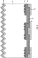
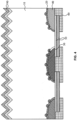
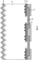
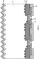
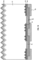
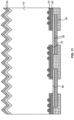
- FIG. 1 to FIG. 7 and FIG. 9 to FIG. 11 are structural schematic diagrams of various implementations of a selective contact region buried solar cell provided by embodiments not covered by the claims but useful for understanding the invention ;
- Fig. 8 is a structural schematic diagram of an implementation of a selective contact region buried solar cell according to an embodiment of the invention ;
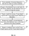
- FIG. 12 is a flow chart of a selective contact region buried solar cell manufacturing method provided by an embodiment not covered by the claims but useful for understanding the invention.
- recesses are disposed at intervals on a back of a silicon substrate, and P-type doped regions and N-type doped regions are disposed alternately inside the recesses, so that separation between the P-type doped regions and the N-type doped regions inside the recesses is implemented through a protrusion structure of the silicon substrate itself between the recesses; moreover, the recesses disposed have a higher tolerance in width control requirement than existing trenches, and preparation of the recesses is easier than preparation of the existing trenches. Further, when a first dielectric layer, P-type doped regions and N-type doped regions are deposited in the recesses, the deposition effect is better because of the higher tolerance in width control.
- the carriers generated on the silicon substrate would also be easily separated through the first dielectric layer on the sidewalls of the recesses and selectively collected into the corresponding P-type doped regions and N-type doped regions, so that current leakage can be reduced and selective transport of the carriers in longitudinal and transverse directions can also be implemented, thereby facilitating multi-dimensional collection of the carriers on the bottom walls and sidewalls of the recesses.
- a second dielectric layer disposed has at least one layer, multi-layer induced passivation is achieved at the back surface of the silicon substrate through the second dielectric layer having at least one layer, and inner back reflection is enhanced, thereby yielding a better passivation effect and a better inner back reflection effect and solving the existing problems of a high trench width control requirement and a poor passivation effect.
- the first embodiment of the disclosure provides a back contact structure of a solar cell. To facilitate explanation, merely the parts related to the embodiment of the disclosure are illustrated. With reference to FIG. 1 to FIG. 11 , the back contact structure of the solar cell provided by the embodiment of the disclosure comprises:
- the silicon substrate 10 has a front facing the sun and a back opposite to the front during a normal working period, and the front is an illuminated face; the back is disposed on the other side of the silicon substrate 10 with respect to the front, i.e., the front and the back are located on different sides, i.e., opposite sides, of the silicon substrate 10, where in this embodiment, the silicon substrate 10 is an N-type silicon slice, and it can be understood that, in other embodiments, the silicon substrate 10 may also be another silicon slice.
- the recesses are formed at intervals on the back surface of the silicon substrate 10; the recesses can be formed through laser ablation or through a combination of a mask (such as a hard mask, a silicon oxide mask, a silicon nitride mask, and a photoresist mask) and wet/dry etching; in this case, due to the recesses formed at intervals on the back surface of the silicon substrate 10, a region between two adjacent recesses located on the silicon substrate 10 is roughly in a protrusion shape, and thus a back pattern of the silicon substrate 10 generally appears to be formed by staggering the recesses and protrusions.
- a mask such as a hard mask, a silicon oxide mask, a silicon nitride mask, and a photoresist mask
- the first dielectric layer 20 is located at the back surface of the silicon substrate 10 and at least covers each recess; during specific implementation, the first dielectric layer 20 covers each recess or covers the entire back surface of the silicon substrate 10. In an embodiment of the disclosure, as shown in FIG. 1 , the first dielectric layer 20 only covers the recesses. In another embodiment of the disclosure, as shown in FIG. 2 , the first dielectric layer 20 covers the entire back surface of the silicon substrate 10, i.e., the first dielectric layer 20 thereof covers the recesses and protrusions of the silicon substrate 10. It should be indicated that, as shown in FIG. 1 and FIG. 2 , the first dielectric layer 20 covering the recesses specifically refers to covering the bottom walls and sidewalls of the recesses, and at this time, the first dielectric layer 20 is connected to the bottom walls and sidewalls of the recesses.
- the first dielectric layer 20 and the P-type doped regions 30 are disposed inside a recess
- the first dielectric layer 20 and the N-type doped regions 40 are disposed inside the another adjacent recess, so that the first dielectric layer 20 and the P-type doped regions 30 as well as the first dielectric layer 20 and the N-type doped regions 40 are disposed alternately in the recesses, where the first dielectric layer 20 is located between the silicon substrate 10 and the P-type doped regions 30 or the N-type doped regions 40 disposed in the recesses, and is used as a tunneling structure; moreover, the first dielectric layer 20 and the highly doped P-type doped regions 30 or N-type doped regions 40 connected thereto and covered thereby together form a passivated contact structure.
- the passivated contact structure provides good surface passivation for the back surface of the silicon substrate 10; in addition, generally speaking, the first dielectric layer 20 has a thin enough thickness, in which one type of the carriers achieves selective transmission through a tunneling principle, while another type of the carriers is hard to tunnel through the first dielectric layer 20 due to the existence of a barrier and a doped region field effect. Therefore, the first dielectric layer 20 may allow one type of the carriers to tunnel through and enter the doped regions while blocking another type of the carriers from passing through to cause composition, so that interface composition can be obviously reduced, the solar cell has relatively high open-circuit voltage and short-circuit current, and then photovoltaic conversion efficiency is improved. Meanwhile, as shown in FIG. 1 to FIG.
- a plurality of inner diffusion regions corresponding to the P-type doped regions 30 or N-type doped regions 40 are formed on the surface of the silicon substrate 10 in contact with the first dielectric layer 20; for example, a plurality of P+ inner diffusion regions are formed on the surface of the silicon substrate 10 in contact with the recesses provided with the first dielectric layer 20 and the P-type doped regions 30; for example, a plurality of N+ inner diffusion regions are formed on the surface of the silicon substrate 10 in contact with the recesses provided with the first dielectric layer 20 and the N-type doped regions 40.
- the carriers generated on the silicon substrate 10 would also be easily separated through the first dielectric layer 20 on the sidewalls of the recesses and selectively collected into the corresponding P-type doped regions 30 or N-type doped regions 40, thereby facilitating multi-dimensional collection of the carriers on the bottom walls and sidewalls of the recesses.
- the first dielectric layer 20 is preferably one of a tunneling oxide layer, an intrinsic silicon carbide layer and an intrinsic amorphous silicon layer, or a combination thereof.
- the first dielectric layer 20 may be a tunneling oxide layer of a single material, may also be a combination of a tunneling oxide layer and the intrinsic amorphous silicon layer of multiple materials, and may further be a combination of multiple layers of intrinsic amorphous silicon having different refractive indexes of a single material.
- the specific structural arrangement of the first dielectric layer 20 comprises, but not limited to, the several modes listed above, and according to actual usage needs, the first dielectric layer 20 is correspondingly configured, which is not specifically limited herein.
- the first dielectric layer 20 is preferably the tunneling oxide layer and the intrinsic silicon carbide layer; in this case, the tunneling oxide layer and the intrinsic silicon carbide layer are successively arranged outward from the silicon substrate 10, the tunneling oxide layer is in contact with the back surface of the silicon substrate 10 inside the recesses, and the intrinsic silicon carbide layer is in contact with the P-type doped regions 30 or the N-type doped regions 40.
- the tunneling oxide layer preferably comprises one or more of a silicon oxide layer and an aluminum oxide layer.
- the first dielectric layer 20 may also be a combination of the silicon oxide layer and the aluminum oxide layer in the tunneling oxide layer.
- the intrinsic silicon carbide layer in the first dielectric layer 20 comprises an intrinsic hydrogenated silicon carbide layer.
- the tunneling oxide layer and the intrinsic silicon carbide layer reduce the density of interface states between the silicon substrate 10 and the N-type doped regions 40 as well as the P-type doped regions 30 through chemical passivation.
- hydrogen in the intrinsic hydrogenated silicon carbide layer enters the silicon substrate 10 under the function of a diffusion mechanism and a thermal effect, to neutralize dangling bonds of the back surface of the silicon substrate 10, to passivate defects of the back surface of the silicon substrate 10, and to transfer an energy band in a forbidden band to a valence band or a conduction band to improve probability for the carriers to enter the P-type doped regions 30 or the N-type doped regions 40 through the first dielectric layer 20.
- the first dielectric layer 20 preferably adopts the silicon oxide layer of 1-2 nm and the intrinsic silicon carbide layer of 2-5 nm; as compared with only using the silicon oxide layer as the tunneling structure, the intrinsic silicon carbide layer may further provide an additional hydrogen passivation effect; a preparing process window of the tunneling structure is enlarged, without influencing the tunneling effect; certainly, the silicon oxide layer of 1-2 nm, or the silicon oxide layer of 1 nm and the aluminum oxide layer of 1 nm, or two or more of the intrinsic silicon carbide layers having different refractive indexes can also be directly adopted; as can be understood, the specific structure arrangement of the first dielectric layer 20 comprises, but not limited to, the several specific examples listed above.
- the first dielectric layer 20 may also be an intrinsic microcrystalline silicon layer, an intrinsic microcrystalline silicon oxide layer, an intrinsic amorphous silicon oxide layer, etc. As shown in FIG. 1 to FIG. 11 , it is only shown that the first dielectric layer 20 is a one-layer structure; as can be understood, the specific structure of the first dielectric layer 20 is set according to actual needs and does not completely follow the accompanying drawings of the description.
- the structure of the first dielectric layer 20 disposed on the recesses can be selected to be same or different, which specifically is: the first dielectric layer 20 corresponding to the P-type doped regions 30 is the same as or different from the first dielectric layer 20 corresponding to the N-type doped regions 40; for example, all of the first dielectric layers 20 may be selected as the silicon oxide layer and the intrinsic silicon carbide layer; the first dielectric layer 20 in the recesses provided with the P-type doped regions can also be the silicon oxide layer and the intrinsic silicon carbide layer, and the first dielectric layer 20 in the recesses provided with the N-type doped regions comprises the aluminum oxide layer and the intrinsic silicon carbide layer. According to actual usage needs, a film layer structure of the first dielectric layer 20 on each recess is correspondingly set, which is not specifically limited herein.
- the P-type doped regions 30 and the N-type doped regions 40 are respectively disposed inside the recesses; the P-type doped regions 30 and the N-type doped regions 40 preferably comprise the doped polycrystalline silicon or doped silicon carbide or doped amorphous silicon, where the doped silicon carbide may comprise doped hydrogenated silicon carbide, and the doped hydrogenated silicon carbide is specifically formed by adding hydrogen when depositing the silicon carbide. It should be indicated that when the first dielectric layer 20 comprises the silicon oxide layer and the intrinsic silicon carbide layer above, the plurality of P-type doped regions 30 and the plurality of N-type doped regions 40 are specifically doped silicon carbide.
- the P-type doped regions 30 and the N-type doped regions 40 may be doped polycrystalline silicon or the like.
- the P-type doped regions 30 and the N-type doped regions 40 are specifically doped amorphous silicon.
- the P-type doped regions 30 and the N-type doped regions 40 may be selected to be the same or different, for example, the P-type doped regions 30 and the N-type doped regions 40 are all doped polycrystalline silicon; or the P-type doped regions 30 are doped polycrystalline silicon, and the N-type doped regions 40 are doped silicon carbide, or the like; according to actual usage needs, the P-type doped regions 30 and the N-type doped regions 40 are correspondingly set, which is not specifically limited herein.
- the second dielectric layer 50 covers regions between the recesses of the silicon substrate 10, or extends to cover the P-type doped regions 30 and/or the N-type doped regions 40. That is to say, the second dielectric layer 50 may only cover the protrusions of the silicon substrate 10, as shown in FIG. 3 ; correspondingly, in this case, the conductive layer 60 covers the entire back of the P-type doped regions 30 and the N-type doped regions 40 for electrical connection. The second dielectric layer 50 may also extend from the protrusions to cover the P-type doped regions 30 and/or the N-type doped regions 40, see FIG.
- the second dielectric layer 50 may extend from the protrusions to cover part of regions of the P-type doped regions 30, or extend from the protrusions to cover part of regions of the N-type doped regions 40, or extend from the protrusions to cover part of the regions of the P-type doped regions 30 and the N-type doped regions 40, and in this case, the conductive layer 60 covers the remaining part of the back that does not cover the second dielectric layer 50 in the P-type doped regions 30 and the N-type doped regions 40 to form electrical connections to the P-type doped regions 30 and the N-type doped regions 40, respectively.
- the entire back of the back contact structure can also be completely covered, and in this case, when preparing the conductive layer 60, the conductive layer 60 penetrates through the second dielectric layer 50 by means of perforation or the like to form electric connections to the P-type doped regions 30 and the N-type doped regions 40, respectively.
- the second dielectric layer 50 at least covers the protrusion of the silicon substrate 10; at this time, the second dielectric layer 50 is in direct contact with the back of the protrusion of the silicon substrate 10 at the protrusions, as shown in FIG. 1 .
- the second dielectric layer 50 at least covers the first dielectric layer 20 at the protrusion of the silicon substrate 10, and at this time, the second dielectric layer 50 is in contact with the first dielectric layer 20, as shown in FIG. 2 .
- the second dielectric layer 50 can extend to cover the P-type doped regions 30 and/or the N-type doped regions 40.
- the second dielectric layer 50 is preferably selected from one of an aluminum oxide layer, a silicon nitride layer, a silicon oxynitride layer, an intrinsic silicon carbide layer, an intrinsic amorphous silicon layer and a silicon oxide layer, or a combination thereof.
- the second dielectric layer 50 plays a passivation function and the second dielectric layer 50 is at least set as a one-layer structure; the refractive index of each layer is set to successively decrease outward from the silicon substrate 10, so that the film layer adjacent to the silicon substrate 10 plays a passivation function, while the film layer away from the silicon substrate 10 plays an anti-reflection function, to enhance the anti-reflection effect, thereby increasing the absorption and usage of light by the silicon substrate 10, to increase the short-circuit current density.
- the second dielectric layer 50 may further be a doped silicon layer (such as a doped microcrystalline silicon layer, a doped amorphous silicon layer, and a doped polycrystalline silicon layer), a doped silicon carbide layer (such as a doped polycrystalline silicon carbide layer), a doped silicon oxide layer (such as a doped polycrystalline silicon oxide and doped amorphous silicon oxide), etc.
- a doped silicon layer such as a doped microcrystalline silicon layer, a doped amorphous silicon layer, and a doped polycrystalline silicon layer
- a doped silicon carbide layer such as a doped polycrystalline silicon carbide layer
- a doped silicon oxide layer such as a doped polycrystalline silicon oxide and doped amorphous silicon oxide
- each film layer of a different structure in the second dielectric layer 50 may comprise a plurality of films with different refractive indexes, and according to the fact that the refractive index of each film layer is set to successively decrease outward from the silicon substrate 10, for example, the silicon oxide layer in the second dielectric layer 50 may comprise a plurality of silicon oxide film layers having the refractive index successively decreasing outward from the silicon substrate 10.
- the second dielectric layer 50 may be a three-layer structure comprising the silicon oxide layer/aluminum oxide layer, intrinsic silicon carbide layer, and silicon nitride layer/silicon oxynitride layer; in this case, the thickness of the silicon oxide layer/aluminum oxide layer located at a first layer at an inner side is greater than 0.5 nm, the thickness of the intrinsic silicon carbide layer located at a second layer is greater than 1 nm, and the thickness of the silicon nitride layer/silicon oxynitride layer located at a third layer at an outer side is greater than 50 nm.
- the second dielectric layer 50 may further be a two-layer structure comprising the aluminum oxide layer, and silicon nitride layer/silicon oxynitride layer; in this case, the thickness of the aluminum oxide layer located at a first layer at an inner side is greater than 1 nm, and the thickness of the silicon nitride layer/silicon oxynitride layer located at a second layer at an outer side is greater than 50 nm.
- the second dielectric layer 50 may further be a three-layer structure comprising the silicon oxide layer/aluminum oxide layer, doped polycrystalline silicon layer/doped polycrystalline silicon carbide layer/doped polycrystalline silicon oxide layer, and silicon nitride layer/silicon oxynitride layer, in this case, the thickness of the silicon oxide layer/aluminum oxide layer located at a first layer at an inner side is 0.5-3 nm, the thickness of the doped polycrystalline silicon layer/doped polycrystalline silicon carbide layer/doped polycrystalline silicon oxide layer located at a second layer is 20-100 nm, and the thickness of the silicon nitride layer/silicon oxynitride layer located at a third layer at an outer side is greater than 50 nm.
- the second dielectric layer 50 may further be a three-layer structure comprising the intrinsic amorphous silicon layer, doped amorphous silicon layer/doped amorphous silicon oxide layer, and silicon nitride layer/silicon oxynitride layer; in this case, the thickness of the intrinsic amorphous silicon layer located at a first layer at an inner side is 2-10 nm, the thickness of the doped amorphous silicon layer/doped amorphous silicon oxide layer located at a second layer is 2-50 nm, and the thickness of the silicon nitride layer/silicon oxynitride layer located at a second layer at an outer side is greater than 50 nm.
- the second dielectric layer 50 may further be a three-layer structure comprising the silicon oxide/aluminum oxide layer, intrinsic silicon carbide layer/doped amorphous silicon oxide layer, and silicon nitride layer/silicon oxynitride layer; in this case, the thickness of the silicon oxide/aluminum oxide layer located at a first layer at an inner side is 0.5-3 nm, the thickness of the intrinsic silicon carbide layer/doped amorphous silicon oxide layer located at a second layer is 10-50 nm, and the thickness of the silicon nitride layer/silicon oxynitride layer located at a second layer at an outer side is greater than 50 nm.
- the specific structure arrangement of the second dielectric layer 50 comprises, but not limited to, several specific examples listed above.
- the second dielectric layer 50 is preferably a two-layer structure of an aluminum oxide layer and an intrinsic silicon carbide layer or a two-layer structure of a silicon oxide layer and an intrinsic silicon carbide layer, and in this case, the overall thickness of the second dielectric layer 50 is greater than 25 nm, where it is normally 70-80 nm during normal production and preparation.
- the intrinsic silicon carbide layer not only provides a hydrogen passivation effect, but also reduces parasitic light absorption due to a large optical band gap and a small absorption coefficient with respect to the intrinsic amorphous silicon layer and the doped polycrystalline silicon layer or the like. Furthermore, the thickness of the aluminum oxide layer or the silicon oxide layer in the second dielectric layer 50 is less than 25 nm, and the thickness of the intrinsic silicon carbide layer in the second dielectric layer 50 is greater than 10 nm. It should be indicated that in the multi-layer structure indicated in the embodiment of the disclosure, the order thereof is to arrange outward from the silicon substrate.
- the second dielectric layer 50 above comprises the aluminum oxide layer and intrinsic silicon carbide layer
- the aluminum oxide layer is close to the silicon substrate, while the intrinsic silicon carbide layer is close to the outer side.
- the second dielectric layer 50 is a two-layer structure; as can be understood, the second dielectric layer 50 may further have other layer number, and the specific structure thereof is set according to actual needs and is not completely as shown in the accompanying drawings of the description.
- the intrinsic silicon carbide layer in the second dielectric layer 50 comprises at least one first intrinsic silicon carbide film.
- the refractive indexes of the first intrinsic silicon carbide films successively decrease outward from the back surface of the silicon substrate 10.
- the refractive index of each material is generally selected as: the refractive index of monocrystalline silicon is 3.88; the refractive index of amorphous silicon is 3.5-4.2; the refractive index of polycrystalline silicon is 3.93; the refractive index of silicon carbide is 2-3.88; the refractive index of silicon nitride is 1.9-3.88; the refractive index of silicon oxynitride is 1.45-3.88; the refractive index of silicon oxide is 1.45; and the refractive index of aluminum oxide is 1.63.
- the refractive index of each material above may further be set as others according to actual usage needs, and is not specifically limited herein.
- a magnesium fluoride layer is disposed at an outer layer of the second dielectric layer 50, i.e., based on the one of an aluminum oxide layer, a silicon nitride layer, a silicon oxynitride layer, an intrinsic silicon carbide layer, an intrinsic amorphous silicon layer and a silicon oxide layer, or a combination thereof selected by the second dielectric layer 50, the magnesium fluoride layer can further be disposed at the outer layer of the second dielectric layer 50.
- the refractive index requirement for the magnesium fluoride layer is the lowest, and generally, the refractive index thereof is set as 1.4, for enhancing the optical function of anti-reflection.
- the conductive layer 60 is a TCO (transparent conductive oxide) film and/or a metal electrode.
- the metal electrode comprises a silver electrode, a copper electrode, an aluminum electrode, a tin-clad copper electrode, or a silver-clad copper electrode.
- the copper electrode is electro-plated copper prepared through an electroplating process or a copper electrode prepared through physical vapor deposition.
- nickel, chromium, titanium, and tungsten electrodes serve as a seed layer or a protective layer.
- the conductive layer 60 is a TCO (transparent conductive oxide) film and a metal electrode
- the conductive layer 60 is a metal electrode.
- the metal electrode made of a low-temperature silver paste can only be applied to the HBC cells manufactured in low-temperature processes.
- the plurality of recesses is in the shape of an arc, a trapezoid, or a square. As shown in FIG. 1 , in a specific embodiment, the plurality of recesses is a square. As shown in FIG. 4 , in another specific embodiment, the recess is in the shape of an arc. As shown in FIG. 5 , in another specific embodiment, the recess is a trapezoid.
- the recess is preferably to be set as an arc or a trapezoid, because when the recess is set as an arc or a trapezoid, an effect of reflecting light by the inner wall of the recess is better, and the surface area of the first dielectric layer 20 specifically as the tunneling structure in contact with the silicon substrate 10 can further be increased.
- each recess maybe the same or different, for example, the recesses of the P-type doped regions 30 and the recesses of the N-type doped regions 40 are all set as square, or the recesses of the P-type doped regions 30 are set as square, and the recesses of the N-type doped regions 40 are set as arc, and the like, and therefore, the shape of each recess is set according to actual usage needs thereof, which is not specifically limited herein.
- the first dielectric layer 20 is connected to the bottom walls of the recesses and the second dielectric layer 50 is further connected to the sidewalls of the recesses.
- this is mainly because that the recess region is covered using the mask, and then when the mask is removed in a subsequent process, silicon in part of the silicon substrate 10 near the plurality of P-type doped regions 30 or plurality of N-type doped regions 40 will be corroded to widen the recess; and when the second dielectric layer 50 is deposited in a subsequent process, the second dielectric layer 50 will be deposited in a blank region, so that the second dielectric layer 50 is connected to the sidewall of the recess.
- an arc-shaped recess (such as an ellipsoid-shaped recess)
- the first dielectric layer 20 and the plurality of P-type doped regions 30 or plurality of N-type doped regions 40 cannot be deposited onto the inner wall of the arc-shaped recess in the long-axis direction, and thus the blank region may be filled with the second dielectric layer 50 during deposition thereof so that the second dielectric layer 50 is connected to the sidewall of the arc-shaped recess, or there may be another case where the second dielectric layer 50 cannot be deposited to the blank region during deposition so that a certain gap is formed between the sidewall of the arc-shaped recess and the first dielectric layer 20 and the plurality of P-type doped regions 30 or plurality of N-type doped regions 40.
- the first dielectric layer 20 is directly connected to the sidewall of the recess, so that the first dielectric layer 20 disposed on the sidewall of the recess can allow selective pass-through of the carriers to achieve multi-dimension collection.
- the thickness of the first dielectric layer 20 is 1-20 nm
- the total thickness of the first dielectric layer 20 and the plurality of P-type doped regions 30 is greater than 20 nm
- the total thickness of the first dielectric layer 20 and the plurality of N-type doped regions 40 is greater than 20 nm.
- the width of the recess of the plurality of P-type doped regions 30 is 300-600 ⁇ m
- the width of the recess of the plurality of N-type doped regions 40 is 100-500 ⁇ m
- the depth of each of the recesses is 0.01-10 ⁇ m
- the between every two adjacent recesses is 20-500 ⁇ m.
- the width of the recess of the plurality of P-type doped regions 30 is preferably set to 500 ⁇ m
- the width of the recess of the plurality of N-type doped regions 40 is preferably set to 300 ⁇ m
- the between every two adjacent recesses is preferably 100 ⁇ m.
- the width control requirement of dozens of microns for the set recess width is looser as compared with the existing trenches; it would be easier to prepare it as compared with preparing the existing trenches. It should be indicated that each of the accompanying drawings of the description is merely used for describing each specific structure distribution in the back contact structure thereof, but it does not correspond to the actual size dimension of each structure.
- the thickness of the first dielectric layer 20 above is 1-20 nm
- the thickness of the second dielectric layer 50 is greater than 25 nm; in the accompanying drawings, they do not completely correspond to the specific actual size dimensions in this embodiment, and should depend on the specific parameters provided in this embodiment.
- the total thickness of the first dielectric layer 20 and the plurality of P-type doped regions 30 and/or the total thickness of the first dielectric layer 20 and the plurality of N-type doped regions 40 disposed in the recess is less than or equal to the depth of the recess.
- the total thickness of the first dielectric layer 20 and the plurality of P-type doped regions 30 and/or the total thickness of the first dielectric layer 20 and the plurality of N-type doped regions 40 disposed in the recess is greater than the depth of the recess.
- multiple combination modes may appear, such as the total thickness of the first dielectric layer 20 and the plurality of P-type doped regions 30 and the total thickness of the first dielectric layer 20 and the plurality of N-type doped regions 40 are both greater than the depth of the recess, both equal to the depth of the recess, and both less than the depth of the recess; or the total thickness of the first dielectric layer 20 and the plurality of P-type doped regions 30 is greater than the depth of the recess, while the total thickness of the first dielectric layer 20 and the plurality of N-type doped regions 40 is less than the depth of the recess; or the total thickness of the first dielectric layer 20 and the plurality of P-type doped regions 30 is less than the depth of the recess while the total thickness of the first dielectric layer 20 and the plurality of N-type doped regions 40 is greater than the depth of the recess.
- the total thickness of the first dielectric layer 20 and the plurality of P-type doped regions 30 and the total thickness of the first dielectric layer 20 and the plurality of N-type doped regions 40 are both equal to the depth of the recess; at this time, the second dielectric layer 50 forms a plane shape while covering the protrusion, P-type doped regions 30, and N-type doped regions 40 of the silicon substrate 10, and separation between the P-type doped regions 30 and the N-type doped regions 40 is implemented through the protrusion of the silicon substrate 10. Moreover, with reference to FIG.
- the total thickness of the first dielectric layer 20 and the plurality of P-type doped regions 30 and the total thickness of the first dielectric layer 20 and the plurality of N-type doped regions 40 are both greater than the depth of the recess; at this time, the second dielectric layer 50 forms a trench while covering the protrusion, P-type doped regions 30, and N-type doped regions 40 of the silicon substrate 10, and at this time, separation between the P-type doped regions 30 and the N-type doped regions 40 is implemented through the protrusion of the silicon substrate 10 and the trench formed by the second dielectric layer 50. Moreover, with reference to FIG.
- the total thickness of the first dielectric layer 20 and the plurality of P-type doped regions 30 and the total thickness of the first dielectric layer 20 and the plurality of N-type doped regions 40 is less than the depth of the recess. At this time, separation between the P-type doped regions 30 and the N-type doped regions 40 is implemented through the protrusion of the silicon substrate 10.
- the P-type doped regions 30 and/or the N-type doped regions 40 can further extend to regions between the recesses, i.e., for example, the P-type doped regions 30 can extend to part or all of the regions between the recesses, and are not in contact with the adjacent N-type doped regions 40; in this case, a passivated contact structure is also formed on the first dielectric layer 20 and the P-type doped regions 30 disposed on the protrusion regions between the recesses; moreover, the first dielectric layer 20 and the P-type doped regions 30 in the recesses are communicated to increase a contact area of the first dielectric
- the first dielectric layer 20 and the N-type doped regions 40 need to be less than the depth of the recess, so that the P-type doped regions 30 extending out from the recesses are not in contact with the adjacent N-type doped regions 40.
- the P-type doped regions 30 and the N-type doped regions 40 extend along a side of the protrusion; as can be understood, the P-type doped regions 30 and/or the N-type doped regions 40 can also extend along two sides of the protrusion; at this time, the P-type doped regions 30 and/or the N-type doped regions 40 extending on the protrusion are not connected to the adjacent N-type doped regions 40 and/or P-type doped regions 30.
- first doped layers 70 are disposed in part or all of the silicon substrate 10 located on regions between the recesses. That is to say, the first doped layers 70 are disposed on the protrusions of the silicon substrate 10, where the first doped layers 70 may be disposed on the protrusions taken as a whole and may also be disposed on part of the regions of the protrusions.
- the first doped layer 70 is specifically a diffusion layer.
- the diffusion layer is a diffusion layer formed by doping different types of diffusion sources on the silicon substrate 10 of the protrusions, and thus is a diffusion layer formed by partially diffusing the silicon substrate 10 of the protrusions.
- the diffusion layer may be a P-type diffusion layer or an N-type diffusion layer, where the P-type diffusion layer is formed by diffusion of doped boron, aluminum, gallium or the like, and the N-type diffusion layer is formed by diffusion of doped nitrogen, phosphorus, arsenic or the like.
- the N-type diffusion layer is an N+ layer with respect to the silicon substrate 10 which is specifically an N-type silicon slice, i.e., the diffusion layer is formed by local heavy diffusion.
- the first doped layer 70 disposed on the protrusions of the silicon substrate 10 may be correspondingly set as the P-type diffusion layers or the N-type diffusion layers depending on actual usage needs, which is not specifically limited herein.
- the P-type diffusion layers and the N-type diffusion layers are formed by alternately performing different types of diffusion on the protrusions of the silicon substrate 10.
- the first dielectric layer 20 is disposed on the sidewalls of the recesses and the first doped layer 70 is formed by performing diffusion in regions between the recesses in the silicon substrate 10, it would be easier for the carriers in a first doped layer 70 to selectively pass through the first dielectric layer 20 on the sidewall of the adjacent recess to be separated and collected into the corresponding plurality of P-type doped regions 30 or plurality of N-type doped regions 40.
- a back surface of the silicon substrate 10 located on regions between the recesses comprises a rough texture structure 80. That is to say, the protrusion surface of the silicon substrate 10 thereof has the rough texture structure 80, where when the first dielectric layer 20 merely covers the recesses, the rough texture structure 80 is located at a position where the second dielectric layer 50 is in contact with the back surface of the silicon substrate 10; when the first dielectric layer 20 covers the back of the entire silicon substrate 10, the rough texture structure 80 is located at a position where the first dielectric layer 20 is in contact with the back surface of the silicon substrate 10.
- the rough texture structure 80 is generally made through texturing, comprising forming hemispherical textures through acid texturing and forming pyramid-shaped textures through alkaline texturing, or forming pyramid-shaped textures through alkaline texturing and then performing rounding treatment on pyramid apexes through acid texturing. It should be understood that the rough texture structure 80 may also be disposed on the entire back surface of the silicon substrate 10, that is, the silicon substrate 10 inside the recesses also has the rough texture structure 80. In this case, the entire back surface of the silicon substrate 10 on which the recesses are formed is directly textured, without the subsequent process of removing the rough texture structure 80 inside the recesses, so that the process is simplified.
- the second embodiment of the disclosure provides a selective contact region buried solar cell.
- the selective contact region buried solar cell provided by the embodiment of the disclosure comprises:
- the second dielectric layer 50 and the third dielectric layer 90 may be respectively prepared on the front and back surface of the silicon substrate 10 through the same process.
- the third dielectric layer 90 may have the same structure as the second dielectric layer 50 in the foregoing embodiment. Therefore, with reference to the foregoing embodiment, preferably, the third dielectric layer 90 may also be selected from one of an aluminum oxide layer, a silicon nitride layer, a silicon oxynitride layer, an intrinsic silicon carbide layer, an intrinsic amorphous silicon layer and a silicon oxide layer, or a combination thereof.
- the third dielectric layer 90 may further have a three-layer structure comprising the silicon oxide layer/aluminum oxide layer and the doped polycrystalline silicon layer/doped polycrystalline silicon carbide layer/doped polycrystalline silicon oxide layer and the silicon nitride layer/silicon oxynitride layer, or a three-layer structure comprising the intrinsic amorphous silicon layer and the doped amorphous silicon layer/doped amorphous silicon oxide layer and the silicon nitride layer/silicon oxynitride layer, or a three-layer structure comprising the silicon oxide layer/aluminum oxide layer and the silicon carbide layer/doped amorphous silicon oxide layer and the silicon nitride layer/silicon oxynitride layer.
- the third dielectric layer 90 also correspondingly has a two-layer structure comprising the silicon oxide layer and the silicon carbide layer, or a two-layer structure comprising the aluminum oxide layer and the silicon carbide layer, and the thickness of the third dielectric layer 90 is greater than 50 nm.
- the thickness of the aluminum oxide layer or the silicon oxide layer in the third dielectric layer 90 is less than 40 nm, and the thickness of the silicon carbide layer in the third dielectric layer 90 is greater than 10 nm.
- the silicon carbide layer not only provides a hydrogen passivation effect, but also reduces parasitic light absorption due to a large optical band gap and a small absorption coefficient with respect to the intrinsic amorphous silicon layer and the doped polycrystalline silicon layer or the like.
- the silicon carbide layer in the third dielectric layer 90 comprises at least one silicon carbide film.
- the refractive indexes of the silicon carbide films successively decrease outward from the front surface of the silicon substrate 10.
- a magnesium fluoride layer is disposed at an outer layer of the third dielectric layer 90.
- the refractive index requirement for the magnesium fluoride layer at the outermost layer is the lowest, and generally, the refractive index is set as 1.4, for enhancing the optical function of anti-reflection.
- the third dielectric layer 90 may have a different structural arrangement from the second dielectric layer 50 in the foregoing embodiment, and the film structures of the second dielectric layer 50 and the third dielectric layer 90 are correspondingly set depending on actual usage needs, which is not specifically limited herein.
- an electric field layer or a floating junction is disposed between the front surface of the silicon substrate 10 and the third dielectric layer 90, specifically comprising performing phosphorus diffusion on the silicon substrate 10 to obtain the electric field layer or performing boron diffusion to obtain the floating junction.
- the electric field layer or the floating junction serves as a Front-Surface Field (FSF) of the selective contact region buried solar cell.
- recesses are disposed at intervals on a back of a silicon substrate, and P-type doped regions and N-type doped regions are disposed alternately inside the recesses, so that separation between the P-type doped regions and the N-type doped regions inside the recesses is implemented through a protrusion structure between the recesses of the silicon substrate itself; moreover, the recesses disposed have a lower width control requirement than existing trenches, and preparation of the recesses is easier than preparation of the existing trenches. Further, when a first dielectric layer, P-type doped regions and N-type doped regions are deposited in the recesses, the deposition effect is better.
- the carriers generated on the silicon substrate would also be easily separated through the first dielectric layer on the sidewalls of the recesses and selectively collected into the corresponding P-type doped regions and N-type doped regions, so that current leakage can be reduced and selective transport of the carriers in longitudinal and transverse directions can also be implemented, thereby facilitating multi-dimensional collection of the carriers on the bottom walls and sidewalls of the recesses.
- a second dielectric layer disposed has at least one layer, multi-layer passivation is achieved on the back surface of the silicon substrate through the second dielectric layer having at least one layer, and inner back reflection is enhanced, thereby yielding a better passivation effect and a better inner back reflection effect and solving the existing problems of a high trench width control requirement and a poor passivation effect.
- the third embodiment of the disclosure provides a selective contact region buried solar cell manufacturing method. To facilitate explanation, merely the parts related to the embodiment of the disclosure are illustrated. With reference to FIG. 12 , the selective contact region buried solar cell manufacturing method provided by the embodiment of the disclosure is used for preparing the selective contact region buried solar cell as stated in the preceding embodiment, and specifically, the method comprises the following steps.
- a plurality of recesses is formed at intervals on a back of a silicon substrate.
- step S11 it should further comprise pre-treating the silicon substrate.
- the pre-treatment above comprises cleaning the silicon substrate and removing a damaged layer.
- the pre-treatment comprises:
- the recesses may be formed in the following ways: way I: the part where the recesses need to be disposed at intervals is directly slotted through laser and partial silicon crystal is removed from the back surface of the silicon substrate, to form the desired recesses; way II: the silicon substrate is subjected to thermal oxidation treatment so that a silicon oxide layer is formed on the entire surface of the silicon substrate, silicon oxide in part of the regions on the front and back surface of the silicon substrate is removed through laser slotting, and then silicon oxide is removed using an acid (such as HF) through wet etching, to form the desired recesses; way III: a silicon nitride layer is deposited on the back surface of the silicon substrate through PECVD, silicon nitride in part of the region on the back is removed through laser slotting, and then silicon nitride is removed through wet etching, to form the desired recesses; way !V, silicon nitride is deposited on the back surface of the silicon substrate or
- way II is preferably used for forming the recesses, where in way II, the thermal oxidation treatment step specifically comprises: performing dry-oxygen oxidation/steam oxidation/wet-oxygen oxidation (i.e., dry-oxygen + steam) in a quartz tube, where specific reactants comprise oxygen and/or high-purity steam, the reaction pressure is 50-1000 mbar, the reaction temperature is 900-1200°C, and the thickness of silicon oxide prepared from the reaction is greater than 10 nm.
- dry-oxygen oxidation/steam oxidation/wet-oxygen oxidation i.e., dry-oxygen + steam
- specific reactants comprise oxygen and/or high-purity steam
- the reaction pressure is 50-1000 mbar
- the reaction temperature is 900-1200°C
- the thickness of silicon oxide prepared from the reaction is greater than 10 nm.
- the step of removing silicon oxide through laser slotting specifically comprises: removing silicon oxide to be removed through slotting by laser having a laser wavelength of 532 nm, a laser power of 10-60 W, a laser frequency less than or equal to 250-1500 KHz, and a laser pulse width of 3-50 ns.
- An alkaline solution and isopropyl acetone are used in the wet etching step, where the alkaline solution is KOH or TMAH, the concentration of the alkaline solution is 1-5%, the content of isopropyl acetone is 1-10%, the reaction temperature is 60-85°C, and the reaction time is 10-30 min.
- An acidic solution in the step of removing silicon oxide using the acid is HF, where the concentration of the acidic solution is 1-5%, the reaction temperature is room temperature, and the reaction time is 3-10 min.
- the depth of the formed recess is 0.01-10 ⁇ m
- the between every two adjacent recesses is 20-500 ⁇ m
- the recess width for preparing the subsequent P-type doped regions is opened as 300-600 ⁇ m
- the recess width for preparing the subsequent N-type doped regions is opened as 100-500 ⁇ m.
- the formed recess may be an arc, a trapezoid, or a square. Since trenches used in the prior art are prepared by laser perforation or wet etching, the width control requirement for the trenches is high and it is difficult to prepare. However, preparation of the recesses in this embodiment is easier than preparation of existing trenches, and does not have a strict width control requirement as the existing trenches.
- Step S21 a first dielectric layer is prepared on the back surface of the silicon substrate, the first dielectric layer at least covering the recesses.
- the specific production process may further comprise texturing the front surface of the silicon substrate.
- texturing on the front is mainly achieved by corrosion using an alkaline solution, where the alkaline solution reacts with the silicon substrate to generate a water-soluble compound, and a pyramid-shaped textured structure is formed on the surface.
- the incident light is used for multiple times, thereby reducing the reflectivity of the front.
- the front and back surface of the silicon substrate can be textured at the same time; and when the back surface of the silicon substrate does not need to have a rough texture structure, a silicon nitride protection layer is deposited on the back surface of the silicon substrate, the front is then textured, and the silicon nitride protection layer is removed from the back through laser, thereby avoiding texturing on the back surface of the silicon substrate.
- the first dielectric layer is prepared on the back surface of the silicon substrate according to a high-temperature oxidation process, a deposition process or the like, which is set depending on the type of the first dielectric layer to be specifically deposited and is not specifically limited therein.
- the first dielectric layer is one of a tunneling oxide layer, an intrinsic silicon carbide layer and an intrinsic amorphous silicon layer, or a combination thereof, and the thickness of the first dielectric layer is 1-20 nm.
- the first dielectric layer coves the entire back surface of the silicon substrate.
- the first dielectric layer covering the protrusions of the silicon substrate can be removed through laser.
- Step S31 P-type doped regions and N-type doped regions disposed alternately are prepared inside the recesses.
- the preparing, inside the recesses, P-type doped regions and N-type doped regions disposed alternately comprises two deposition modes for preparation, i.e., in-situ deposition and ex-situ deposition.
- step S31 when adopting in-situ deposition, comprises:
- the recesses are shielded through the mask to perform in-situ deposition with N-type amorphous silicon/N-type amorphous silicon carbide on the adjacent recesses; and after the P-type amorphous silicon/P-type amorphous silicon carbide and the N-type amorphous silicon/N-type amorphous silicon carbide are alternately deposited inside the recesses, the temperature is increased to 700-1000°C directly using a high-temperature or laser heating method.
- the P-type amorphous silicon/P-type amorphous silicon carbide and the N-type amorphous silicon/N-type amorphous silicon carbide inside the recesses are changed into P-type polycrystalline silicon/P-type silicon carbide and N-type polycrystalline silicon/N-type silicon carbide, to obtain the P-type doped regions and the N-type doped regions.
- the mask may be a hard mask, a silicon nitride mask, a silicon oxide mask, a photoresist mask, etc.
- in-situ deposition of the P-type doped regions is performed on the entire back surface of the silicon substrate.
- P-type amorphous silicon/P-type amorphous silicon carbide is deposited on the entire back surface of the silicon substrate; the P-type amorphous silicon/P-type amorphous silicon carbide on the other regions other than the adjacent recesses that require deposition in the silicon substrate is removed through laser ablation; N-type amorphous silicon/N-type amorphous silicon carbide is deposited on the entire back surface of the silicon substrate; then the N-type amorphous silicon/N-type amorphous silicon carbide on the other regions other than the adjacent recesses that require deposition in the silicon substrate is removed through laser ablation; and then the temperature is increased to 700-1000°C directly using a high-temperature or laser heating method.
- the P-type amorphous silicon/P-type amorphous silicon carbide and the N-type amorphous silicon/N-type amorphous silicon carbide inside the recesses are changed into P-type polycrystalline silicon/P-type silicon carbide and N-type polycrystalline silicon/N-type silicon carbide, to obtain the P-type doped regions and the N-type doped regions.
- step S31 when adopting ex-situ deposition, comprises:
- the step of alternately performing different doping types of doping inside the recesses specifically comprises:
- intrinsic amorphous silicon or intrinsic silicon carbide is deposited inside the recesses; different types of ions are partially injected inside the recesses, for example, P-type ions containing elements such as boron, aluminum, gallium or the like are injected inside the recesses requiring plurality of P-type doped regions preparation, while N-type ions containing elements such as nitrogen, phosphorus, arsenic or the like are injected inside the adjacent recesses; and then high-temperature crystallization treatment is performed so that the original intrinsic amorphous silicon or original intrinsic silicon carbide is changed into doped polycrystalline silicon or doped silicon carbide. Since in deposition with intrinsic amorphous silicon/intrinsic silicon carbide, deposition may be performed on the sides and front surface of the silicon substrate, after high-temperature crystallization, it is required to add wet etching treatment to achieve bypass plating.
- intrinsic amorphous silicon or intrinsic silicon carbide is first deposited inside the recesses; different doping types of doping sources are deposited inside the different recesses with a mask method for doping, for example, when P-type doping sources containing boron, aluminum, gallium or the like (such as borosilicate glass) are deposited inside the recesses requiring plurality of P-type doped regions preparation for doping to form P-type amorphous silicon/P-type silicon carbide, and N-type doping sources containing nitrogen, phosphorus, arsenic or the like (such as phosphosilicate glass) are deposited inside the recesses where plurality of N-type doped regions preparation is required for doping to form N-type amorphous silicon/N-type silicon carbide; and after the P-type doping sources and the N-type doping sources are alternately deposited inside the recesses, high-temperature crystallization treatment is performed so that the original intrinsic amorphous silicon or intrinsic silicon carb
- the mask comprises a hard mask, a silicon nitride mask, a silicon oxide mask, a photoresist mask, etc.
- the masks is specifically a hard mask, for example, the adjacent recesses where no deposition of the P-type doping source is required is first covered through the hard mask, and after the P-type doping source is deposited in the recess wherein deposition of the P-type doping source is required, then further through the hard mask, the recesses thereof are covered, so that the N-type doping source is deposited in the adjacent recesses, to implement depositing different doping sources inside different recesses for doping.
- the mask is specifically the silicon nitride mask
- silicon nitride is first deposited on the back; the recesses where deposition is required are then perforated through laser perforation to remove silicon nitride in the recesses; then after a P-type doping source is deposited in the recesses where deposition is required, silicon oxide is continuously deposited on the back so that silicon nitride covers the P-type doping source for protection; the adjacent recesses are then perforated through laser perforation to remove silicon nitride and the P-type doping source inside the adjacent recesses; then an N-type doping source is deposited in the adjacent recesses, and after the N-type doping source is deposited, the N-type doping source and silicon nitride deposited in the recesses are removed through laser perforation, so that different doping sources are deposited inside different recesses for doping.
- the silicon oxide mask is similar to the silicon nitride mask, and thus is no
- intrinsic amorphous silicon or intrinsic silicon carbide is deposited inside the recesses; different source gases are introduced inside different recesses with a mask method for doping, for example, P-type source gases containing elements such as boron, aluminum, gallium or the like (such as a borane gas or a carrier gas carrying boron trichloride or boron tribromide) are introduced inside the recesses where P-type doping region preparation is required for doping to form P-type amorphous silicon/P-type silicon carbide, and then N-type source gases containing elements such as nitrogen, phosphorus, arsenic or the like (such as a phosphorane gas or a carrier gas carrying phosphorus oxychloride) are introduced inside the recesses where N-type doping region preparation is required for doping to form N-type amorphous silicon/N-type silicon carbide; and after different doping types of the P-type source gas and the N-type source gas are alternately introduced inside the
- step S31 when adopting ex-situ deposition, may further comprise:
- intrinsic amorphous silicon or intrinsic silicon carbide is deposited inside the recesses; and then boron diffusion is directly performed inside the recesses where P-type doping regions are required with a mask method to form the P-type doped regions, and phosphorus diffusion is performed inside the recesses where N-type doping regions are required to form the N-type doped regions.
- the mask comprises a hard mask, a silicon nitride mask, a silicon oxide mask, a photoresist mask, etc.
- the specific implementation may refer to the preceding text.
- the thin first dielectric layer may be partially broken.
- attachment may occur at the broken part of the first dielectric layer and the back surface of the silicon substrate, and then a plurality of inner diffusion regions corresponding to the P-type doped regions or the N-type doped regions are formed on the surface of the silicon substrate in contact with the first dielectric layer.
- the P-type doped regions and the N-type doped regions are alternately prepared inside the recesses, where the plurality of P-type doped regions and the plurality of N-type doped regions comprise doped polycrystalline silicon or doped silicon carbide or doped amorphous silicon; and the total thickness of the first dielectric layer and the plurality of P-type doped regions is greater than 20 nm and the total thickness of the first dielectric layer and the plurality of N-type doped regions is greater than 20 nm.
- a second dielectric layer and a third dielectric layer are respectively prepared on the back and front surface of the silicon substrate.
- the method may further comprise: alternately performing different types of diffusion on the positions on the back protrusions of the silicon substrate, to obtain different types of the first doped layers by diffusion on the positions of the protrusions on the back surface of the silicon substrate.
- the specific preparation process comprises: way I: introducing a source gas containing elements such as boron, aluminum, gallium or the like (such as a borane gas or a carrier gas carrying boron trichloride or boron tribromide) for thermal diffusion to form the P-type diffusion layer; way II: depositing a doping source containing boron, aluminum, gallium or the like (such as borosilicate glass) for thermal diffusion to form the P-type diffusion layer; way III: preparing an aluminum electrode above the diffusion layer and forming the P-type diffusion layer doped with aluminum in a high-temperature process; way IV: spin-coating a doping source containing boron, aluminum, gallium or the
- the specific preparation process comprises: way I: introducing a source gas containing elements such as nitrogen, phosphorus, arsenic or the like (such as a phosphorane gas or a carrier gas carrying phosphorus oxychloride) for thermal diffusion to form the N-type diffusion layer; way II: depositing a doping source containing nitrogen, phosphorus, arsenic or the like (such as phosphosilicate glass) for thermal diffusion to form the N-type diffusion layer; way III: spin-coating a doping source containing nitrogen, phosphorus, arsenic or the like (such as phosphorus oxychloride) for thermal diffusion to form the N-type diffusion layer; and way IV: injecting ions containing elements such as nitrogen, phosphorus, arsenic or the like and performing high-temperature diffusion to form the N-type diffusion layer. It should be indicated that after a doping source is deposited for thermal diffusion, it is also required to remove the doping source through laser or
- the method may further comprise: texturing the positions of the protrusions between the recesses on the back surface of the silicon substrate to obtain the rough texture structure.
- the specific texturing process may refer to the preceding text.
- the preparation is implemented depending on the specific composition types of the second dielectric layer and the third dielectric layer, which is not specifically limited therein.
- the second dielectric layer and the third dielectric layer may be one of an aluminum oxide layer, a silicon nitride layer, a silicon oxynitride layer, an intrinsic silicon carbide layer, an intrinsic amorphous silicon layer and a silicon oxide layer, or a combination thereof.
- the refractive indexes of different silicon carbide films decrease from the front surface of the silicon substrate to outside, and a magnesium fluoride layer having the lowest requirement for the refractive index may be prepared at the outermost layer.
- an electric field layer or a floating junction may be prepared first, specifically comprising performing phosphorus diffusion on the silicon substrate to obtain the electric field layer or performing boron diffusion to obtain the floating junction.
- the electric field layer or the floating junction serves as the FSF of the selective contact region buried solar cell.
- a conductive layer is prepared on the P-type doped regions and the N-type doped regions.
- the conductive layer when the second dielectric layer only covers protrusion regions between the recesses in the silicon substrate, the conductive layer covers the entire back of the P-type doped regions and the N-type doped regions for electrical connection; when the second dielectric layer extends to cover the P-type doped regions and the N-type doped regions, the conductive layer covers the back of the remaining part that does not cover the second dielectric layer in the P-type doped regions and the N-type doped regions; and when the second dielectric layer covers the entire back surface of the silicon substrate, the conductive layer passes through the second dielectric layer as well as the P-type doped regions and the N-type doped regions through perforation or the like for electrical connection, so that first electrodes are formed on the P-type doped regions and second electrodes are formed on the N-type doped regions.
- the conductive layer is the TCO (transparent conductive oxide) film and the metal electrode
- the metal electrode comprises a silver electrode, a copper electrode, an aluminum electrode, a tin-clad copper electrode, or a silver-clad copper electrode.
- the copper electrode is electro-plated copper prepared through an electroplating process or a copper electrode prepared through physical vapor deposition. The electro-plated copper uses nickel, chromium, titanium, and tungsten electrodes as a seed layer or a protection layer thereof.
- the fourth embodiment of the disclosure further provides a cell assembly comprising the selective contact region buried solar cell according to the preceding embodiment.
- recesses are disposed at intervals on a back of a silicon substrate, and P-type doped regions and N-type doped regions are disposed alternately inside the recesses, so that separation between the P-type doped regions and the N-type doped regions inside the recesses is implemented through a protrusion structure between the recesses of the silicon substrate itself; moreover, the recesses disposed have a lower width control requirement than existing trenches, and preparation of the recesses is easier than preparation of the existing trenches. Further, when a first dielectric layer, P-type doped regions and N-type doped regions are deposited in the recesses, the deposition effect is better.
- the carriers generated on the silicon substrate would also be easily separated through the first dielectric layer on the sidewalls of the recesses and selectively collected into the corresponding P-type doped regions and N-type doped regions, so that current leakage can be reduced and selective transport of the carriers in longitudinal and transverse directions can also be implemented, thereby facilitating multi-dimensional collection of the carriers on the bottom walls and sidewalls of the recesses.
- a second dielectric layer disposed has at least one layer, multi-layer passivation is achieved on the back surface of the silicon substrate through the second dielectric layer having at least one layer, and inner back reflection is enhanced, thereby yielding a better passivation effect and a better inner back reflection effect and solving the existing problems of a high trench width control requirement and a poor passivation effect.
- the fifth embodiment of the disclosure further provides a photovoltaic system comprising the cell assembly according to the preceding embodiments.
- recesses are disposed at intervals on a back of a silicon substrate, and P-type doped regions and N-type doped regions are disposed alternately inside the recesses, so that separation between the P-type doped regions and the N-type doped regions inside the recesses is implemented through a protrusion structure between the recesses of the silicon substrate itself; moreover, the recesses disposed have a lower width control requirement than existing trenches, and preparation of the recesses is easier than preparation of the existing trenches.
- the deposition effect is better.
- the carriers generated on the silicon substrate would also be easily separated through the first dielectric layer on the sidewalls of the recesses and selectively collected into the corresponding P-type doped regions and N-type doped regions, so that current leakage can be reduced and selective transport of the carriers in longitudinal and transverse directions can also be implemented, thereby facilitating multi-dimensional collection of the carriers on the bottom walls and sidewalls of the recesses.
- a second dielectric layer disposed has at least one layer, multi-layer passivation is achieved on the back surface of the silicon substrate through the second dielectric layer having at least one layer, and inner back reflection is enhanced, thereby yielding a better passivation effect and a better inner back reflection effect and solving the existing problems of a high trench width control requirement and a poor passivation effect.
Landscapes
- Photovoltaic Devices (AREA)
- Life Sciences & Earth Sciences (AREA)
- Engineering & Computer Science (AREA)
- Sustainable Energy (AREA)
- Sustainable Development (AREA)
Claims (28)
- Structure de contact arrière d'une cellule solaire, dans laquelle la structure de contact arrière comprend :un substrat de silicium (10), le substrat de silicium comprenant une surface arrière comprenant une pluralité d'évidements disposés à intervalles ;une première couche diélectrique (20) disposée directement sur et recouvrant entièrement la paroi inférieure de la pluralité d'évidements, et enfermée dans la pluralité d'évidements ;une pluralité de régions dopées du type P (30) et une pluralité de régions dopées du type N (40) disposées sur la première couche diélectrique (20) et disposées en alternance dans la pluralité d'évidements ;une deuxième couche diélectrique (50) disposée entre la pluralité de régions dopées du type P (30) et la pluralité de régions dopées du type N (40), dans laquelle la deuxième couche diélectrique (50) est au nombre d'au moins une ; etune couche conductrice (60) disposée sur la pluralité de régions dopées du type P (30) et la pluralité de régions dopées du type N respectivement ;dans laquelleune épaisseur totale de la première couche diélectrique (20) et de la pluralité de régions dopées du type P (30) et une épaisseur totale de la première couche diélectrique (20) et de la pluralité de régions dopées du type N (40) disposées dans la pluralité d'évidements sont inférieures à une profondeur de la pluralité d'évidements, et la pluralité de régions dopées du type P (30) et la pluralité de régions dopées du type N (40) sont enfermées à l'intérieur de la pluralité d'évidements ;dans chaque évidement la première couche diélectrique (20) couvre entièrement et est directement sur les parois latérales des évidements à l'exception d'une partie supérieure des parois latérales, la partie des parois latérales couverte par la première couche électrique (20) présentant une hauteur correspondant à l'épaisseur totale de la première couche diélectrique (20) et de la région dopée correspondante (30 et 40) respectivement ;dans chaque évidement la région dopée correspondante (30 et 40) couvre entièrement et est directement sur la première couche diélectrique (20) et remplit l'évidement jusqu'à une hauteur correspondant à l'épaisseur totale de la première couche diélectrique (20) et de la région dopée correspondante (30 et 40) ;la première couche diélectrique (20) correspondant à la région dopée du type P (30) est différente de la première couche diélectrique (20) correspondant à la région dopée du type N (40), etla deuxième couche diélectrique (50) couvre les régions entre les évidements, s'étend pour couvrir la partie supérieure des parois latérales de la pluralité d'évidements qui ne sont pas couvertes par la première couche diélectrique, et s'étend encore pour couvrir partiellement les régions dopées du type P (30) et les régions dopées du type N (40).
- Structure de contact arrière selon la revendication 1, dans laquelle la pluralité de régions dopées du type P (30) et la pluralité de régions dopées du type N (40) comprennent un silicium polycristallin dopé, un carbure de silicium dopé ou un silicium amorphe dopé.
- Structure de contact arrière selon la revendication 1, dans laquelle la première couche diélectrique (20) comprend une couche d'oxyde à effet tunnel, une couche de carbure de silicium intrinsèque, une couche de silicium amorphe intrinsèque, ou une combinaison de celles-ci.
- Structure de contact arrière selon la revendication 1, dans laquelle la deuxième couche diélectrique (50) comprend une couche d'oxyde d'aluminium, une couche de nitrure de silicium, une couche d'oxynitrure de silicium, une couche de carbure de silicium intrinsèque, une couche de silicium amorphe intrinsèque, une couche d'oxyde de silicium, ou une combinaison de celles-ci.
- Structure de contact arrière selon la revendication 1, dans laquelle une partie de la surface arrière du substrat de silicium (10) entre la pluralité d'évidements comprend une structure de texture rugueuse (80).
- Structure de contact arrière selon la revendication 1, dans laquelle une pluralité de premières couches dopées (70) est disposée sur une partie ou la totalité du substrat de silicium (10) situé sur des régions entre la pluralité d'évidements.
- Structure de contact arrière selon la revendication 1, dans laquelle une largeur de la pluralité d'évidements recevant la pluralité de régions dopées du type P (30) est définie à 300-600 µm, une largeur de la pluralité d'évidements recevant la pluralité de régions dopées du type N (40) est définie à 100-500 µm, une profondeur de chacun de la pluralité d'évidements est de 0,01-10 µm, et une distance entre chaque paire d'évidements adjacents est de 20-500 µm.
- Structure de contact arrière selon la revendication 1, dans laquelle la pluralité d'évidements est sous la forme d'un trapézoïde, ou d'un carré.
- Structure de contact arrière selon la revendication 1, dans laquelle une épaisseur de la première couche diélectrique (20) est de 1-20 nm, une épaisseur totale de la première couche diélectrique (20) et de la région dopée du type P (30) est supérieure à 20 nm, et une épaisseur totale de la première couche diélectrique (20) et de la région dopée du type N (40) est supérieure à 20 nm.
- Structure de contact arrière selon la revendication 2, dans laquelle le carbure de silicium dopé comprend un carbure de silicium hydrogéné dopé.
- Structure de contact arrière selon la revendication 3, dans laquelle la première couche diélectrique (20) comprend une combinaison de la couche d'oxyde à effet tunnel et de la couche de carbure de silicium intrinsèque.
- Structure de contact arrière selon la revendication 3 ou 11, dans laquelle la couche d'oxyde à effet tunnel comprend une ou plusieurs d'une couche d'oxyde de silicium et d'une couche d'oxyde d'aluminium.
- Structure de contact arrière selon la revendication 4, dans laquelle la deuxième couche diélectrique (50) comprend une combinaison de la couche d'oxyde d'aluminium et de la couche de carbure de silicium intrinsèque, ou la deuxième couche diélectrique (50) comprend une combinaison de la couche d'oxyde de silicium et de la couche de carbure de silicium intrinsèque, et une épaisseur de la deuxième couche diélectrique (50) est supérieure à 25 nm.
- Structure de contact arrière selon la revendication 13, dans laquelle une épaisseur de la couche d'oxyde d'aluminium ou de la couche d'oxyde de silicium dans la deuxième couche diélectrique (50) est inférieure à 25 nm, et une épaisseur de la couche de carbure de silicium intrinsèque dans la deuxième couche diélectrique (50) est supérieure à 10 nm.
- Structure de contact arrière selon la revendication 4, dans laquelle une couche de fluorure de magnésium est disposée au niveau d'une couche externe de la deuxième couche diélectrique (50).
- Structure de contact arrière selon la revendication 1, dans laquelle la couche conductrice (60) comprend un film d'oxyde conducteur transparent (TCO) et/ou une électrode métallique.
- Structure de contact arrière selon la revendication 16, dans laquelle l'électrode métallique comprend une électrode d'argent, une électrode de cuivre, une électrode d'aluminium, une électrode de cuivre plaquée d'étain, ou une électrode de cuivre plaquée d'argent.
- Structure de contact arrière selon la revendication 17, dans laquelle l'électrode de cuivre est du cuivre électroplaqué préparé par le biais d'un processus d'électroplacage ou une électrode de cuivre préparée par le biais d'un dépôt physique en phase vapeur.
- Structure de contact arrière selon la revendication 7, dans laquelle une première couche diélectrique (20) correspondant aux régions dopées du type P (30) est la même qu'une ou différente d'une première couche diélectrique (20) correspondant aux régions dopées du type N (40).
- Cellule solaire enterrée à région de contact sélective, comprenant :la structure de contact arrière selon l'une quelconque des revendications 1 à 19 ; etune troisième couche diélectrique (90) disposée sur une surface avant du substrat de silicium.
- Cellule solaire enterrée à région de contact sélective selon la revendication 20, dans laquelle la troisième couche diélectrique (90) comprend une couche d'oxyde d'aluminium, une couche de nitrure de silicium, une couche d'oxynitrure de silicium, une couche de carbure de silicium, une couche de silicium amorphe intrinsèque et une couche d'oxyde de silicium, ou une combinaison de celles-ci.
- Cellule solaire enterrée à région de contact sélective selon la revendication 21, dans laquelle la troisième couche diélectrique (90) comprend une combinaison de la couche d'oxyde de silicium et de la couche de carbure de silicium, ou la troisième couche diélectrique (90) comprend une combinaison de la couche d'oxyde d'aluminium et de la couche de carbure de silicium, et une épaisseur de la troisième couche diélectrique (90) est supérieure à 50 nm.
- Cellule solaire enterrée à région de contact sélective selon la revendication 22, dans laquelle une épaisseur de la couche d'oxyde d'aluminium ou de la couche d'oxyde de silicium dans la troisième couche diélectrique (90) est inférieure à 40 nm, et une épaisseur de la couche de carbure de silicium dans la troisième couche diélectrique (90) est supérieure à 10 nm.
- Cellule solaire enterrée à région de contact sélective selon la revendication 21 ou 23, dans laquelle la couche de carbure de silicium dans la troisième couche diélectrique (90) comprend au moins un film de carbure de silicium ; et des indices de réfraction de différents films de carbure de silicium diminuent à partir de la surface avant du substrat de silicium (10) vers l'extérieur.
- Cellule solaire enterrée à région de contact sélective selon la revendication 21, dans laquelle une couche de fluorure de magnésium est en outre disposée sur une couche externe de la troisième couche diélectrique (90).
- Cellule solaire enterrée à région de contact sélective selon la revendication 20, dans laquelle une couche de champ électrique ou une jonction flottante est en outre disposée entre la surface avant du substrat de silicium (10) et la troisième couche diélectrique (90).
- Ensemble cellule, comprenant la cellule solaire enterrée à région de contact sélective selon l'une quelconque des revendications 20 à 26.
- Système photovoltaïque, comprenant l'ensemble cellule selon la revendication 27.
Applications Claiming Priority (1)
| Application Number | Priority Date | Filing Date | Title |
|---|---|---|---|
| CN202110627508.4A CN113299770A (zh) | 2021-06-04 | 2021-06-04 | 一种选择性接触区域掩埋型太阳能电池及其背面接触结构 |
Publications (2)
| Publication Number | Publication Date |
|---|---|
| EP4099408A1 EP4099408A1 (fr) | 2022-12-07 |
| EP4099408B1 true EP4099408B1 (fr) | 2024-03-13 |
Family
ID=77155491
Family Applications (1)
| Application Number | Title | Priority Date | Filing Date |
|---|---|---|---|
| EP21000194.7A Active EP4099408B1 (fr) | 2021-06-04 | 2021-07-23 | Structure de contact et cellule solaire à région de contact sélective arrière enterrée la comprenant |
Country Status (7)
| Country | Link |
|---|---|
| US (1) | US11450777B1 (fr) |
| EP (1) | EP4099408B1 (fr) |
| KR (1) | KR102891080B1 (fr) |
| CN (1) | CN113299770A (fr) |
| DE (1) | DE212021000262U1 (fr) |
| NL (2) | NL2037962B1 (fr) |
| WO (1) | WO2022073626A1 (fr) |
Families Citing this family (17)
| Publication number | Priority date | Publication date | Assignee | Title |
|---|---|---|---|---|
| CN113629157A (zh) * | 2021-08-30 | 2021-11-09 | 浙江爱旭太阳能科技有限公司 | 一种太阳能电池及其接触结构、电池组件及光伏系统 |
| EP4195299A1 (fr) * | 2021-12-13 | 2023-06-14 | International Solar Energy Research Center Konstanz E.V. | Cellule solaire à contact arrière interdigité et procédé de fabrication d'une cellule solaire à contact arrière interdigité |
| CN114420786B (zh) * | 2021-12-22 | 2023-12-05 | 西安隆基乐叶光伏科技有限公司 | 钝化接触电池的制备方法及钝化接触电池 |
| CN114843368B (zh) * | 2022-04-29 | 2024-03-29 | 通威太阳能(成都)有限公司 | 太阳电池及其制备方法和应用 |
| CN116722055A (zh) | 2022-06-27 | 2023-09-08 | 浙江晶科能源有限公司 | 一种太阳能电池及光伏组件 |
| CN116722060A (zh) | 2022-09-28 | 2023-09-08 | 浙江晶科能源有限公司 | 太阳能电池及光伏组件 |
| CN120152440A (zh) * | 2022-10-28 | 2025-06-13 | 天合光能股份有限公司 | 太阳能电池 |
| CN115692516B (zh) * | 2022-11-08 | 2026-03-06 | 正泰新能科技股份有限公司 | 一种新型topcon电池及其制作方法 |
| CN115498057B (zh) * | 2022-11-16 | 2023-04-28 | 金阳(泉州)新能源科技有限公司 | 联合钝化背接触太阳能电池及其基于激光扩散的制备方法 |
| CN118198165A (zh) * | 2022-12-07 | 2024-06-14 | 浙江晶科能源有限公司 | 太阳能电池及其制备方法、光伏组件 |
| CN115954414A (zh) | 2023-02-21 | 2023-04-11 | 浙江晶科能源有限公司 | 一种光伏电池及其制备方法、光伏组件 |
| CN116314400B (zh) * | 2023-05-23 | 2023-09-26 | 浙江爱旭太阳能科技有限公司 | Ibc太阳能电池片、ibc太阳能电池组件和光伏系统 |
| JP7389934B1 (ja) | 2023-03-16 | 2023-11-30 | 浙江愛旭太陽能科技有限公司 | 裏面接触太陽電池セル、裏面接触太陽電池アセンブリ及び太陽光発電システム |
| CN117133834B (zh) * | 2023-10-25 | 2024-02-27 | 金阳(泉州)新能源科技有限公司 | 一种联合钝化背接触电池的短流程制备方法及其应用 |
| CN117497626B (zh) * | 2023-12-14 | 2024-04-23 | 天合光能股份有限公司 | 太阳能电池和太阳能电池的制造方法 |
| CN117727809B (zh) | 2024-02-08 | 2024-08-06 | 浙江晶科能源有限公司 | 太阳能电池及光伏组件 |
| CN119092581A (zh) * | 2024-05-30 | 2024-12-06 | 隆基绿能科技股份有限公司 | 一种半导体结构、太阳能电池及其制造方法、光伏组件 |
Family Cites Families (14)
| Publication number | Priority date | Publication date | Assignee | Title |
|---|---|---|---|---|
| US20110000532A1 (en) * | 2008-01-30 | 2011-01-06 | Kyocera Corporation | Solar Cell Device and Method of Manufacturing Solar Cell Device |
| US7851698B2 (en) | 2008-06-12 | 2010-12-14 | Sunpower Corporation | Trench process and structure for backside contact solar cells with polysilicon doped regions |
| CN102725858B (zh) * | 2010-01-26 | 2015-12-09 | 三洋电机株式会社 | 太阳能电池及其制造方法 |
| US9559228B2 (en) * | 2011-09-30 | 2017-01-31 | Sunpower Corporation | Solar cell with doped groove regions separated by ridges |
| JP2014067804A (ja) * | 2012-09-25 | 2014-04-17 | Sharp Corp | 光電変換素子 |
| US9525083B2 (en) * | 2015-03-27 | 2016-12-20 | Sunpower Corporation | Solar cell emitter region fabrication with differentiated P-type and N-type architectures and incorporating a multi-purpose passivation and contact layer |
| KR102526398B1 (ko) * | 2016-01-12 | 2023-04-27 | 상라오 징코 솔라 테크놀러지 디벨롭먼트 컴퍼니, 리미티드 | 태양 전지 및 이의 제조 방법 |
| JP2019165033A (ja) * | 2016-07-20 | 2019-09-26 | 国立研究開発法人科学技術振興機構 | 太陽電池素子 |
| KR20180031543A (ko) * | 2016-09-19 | 2018-03-28 | 엘지전자 주식회사 | 태양 전지 및 이의 제조 방법 |
| KR102005439B1 (ko) * | 2016-11-23 | 2019-07-30 | 엘지전자 주식회사 | 태양 전지 제조 방법 |
| KR20200108485A (ko) * | 2018-02-02 | 2020-09-18 | 미합중국 (관리부서 : 미합중국 해군성) | 초박형 가요성 후방 접촉 실리콘 태양 전지들 및 이를 제조하기 위한 방법들 |
| KR102600380B1 (ko) * | 2018-12-05 | 2023-11-09 | 상라오 징코 솔라 테크놀러지 디벨롭먼트 컴퍼니, 리미티드 | 태양 전지 및 이의 제조 방법, 그리고 태양 전지 패널 |
| WO2020180244A1 (fr) * | 2019-03-01 | 2020-09-10 | National University Of Singapore | Cellule solaire et procédé de fabrication d'une cellule solaire |
| CN214898459U (zh) * | 2021-06-04 | 2021-11-26 | 浙江爱旭太阳能科技有限公司 | 背面接触结构、太阳能电池、电池组件和光伏系统 |
-
2021
- 2021-06-04 CN CN202110627508.4A patent/CN113299770A/zh active Pending
- 2021-07-23 DE DE212021000262.5U patent/DE212021000262U1/de active Active
- 2021-07-23 KR KR1020247000376A patent/KR102891080B1/ko active Active
- 2021-07-23 EP EP21000194.7A patent/EP4099408B1/fr active Active
- 2021-07-23 WO PCT/EP2021/000083 patent/WO2022073626A1/fr not_active Ceased
- 2021-12-02 US US17/540,275 patent/US11450777B1/en active Active
-
2022
- 2022-06-02 NL NL2037962A patent/NL2037962B1/en active
- 2022-06-02 NL NL2032066A patent/NL2032066B1/en active
Also Published As
| Publication number | Publication date |
|---|---|
| KR102891080B1 (ko) | 2025-11-25 |
| NL2037962A (en) | 2024-07-26 |
| WO2022073626A1 (fr) | 2022-04-14 |
| NL2037962B1 (en) | 2025-12-04 |
| CN113299770A (zh) | 2021-08-24 |
| KR20240022536A (ko) | 2024-02-20 |
| EP4099408A1 (fr) | 2022-12-07 |
| NL2032066B1 (en) | 2024-06-20 |
| US11450777B1 (en) | 2022-09-20 |
| DE212021000262U1 (de) | 2022-07-01 |
| NL2032066A (en) | 2022-12-19 |
Similar Documents
| Publication | Publication Date | Title |
|---|---|---|
| EP4099402B1 (fr) | Structure de contact arrière et région de contact sélective cellule solaire enterrée la comprenant | |
| EP4099408B1 (fr) | Structure de contact et cellule solaire à région de contact sélective arrière enterrée la comprenant | |
| EP4099401B1 (fr) | Structure de contact arrière et cellule solaire à région de contact sélective enterrée la comprenant | |
| EP4099407B1 (fr) | Structure de contact arrière et cellule solaire enterrée à région de contact sélective la comprenant | |
| CN214898462U (zh) | 背面接触结构、太阳能电池、电池组件和光伏系统 | |
| CN214898459U (zh) | 背面接触结构、太阳能电池、电池组件和光伏系统 | |
| CN214898461U (zh) | 背面接触结构、太阳能电池、电池组件和光伏系统 | |
| CN214898463U (zh) | 背面接触结构、太阳能电池、电池组件和光伏系统 |
Legal Events
| Date | Code | Title | Description |
|---|---|---|---|
| STAA | Information on the status of an ep patent application or granted ep patent |
Free format text: STATUS: EXAMINATION IS IN PROGRESS |
|
| PUAI | Public reference made under article 153(3) epc to a published international application that has entered the european phase |
Free format text: ORIGINAL CODE: 0009012 |
|
| 17P | Request for examination filed |
Effective date: 20210810 |
|
| AK | Designated contracting states |
Kind code of ref document: A1 Designated state(s): AL AT BE BG CH CY CZ DE DK EE ES FI FR GB GR HR HU IE IS IT LI LT LU LV MC MK MT NL NO PL PT RO RS SE SI SK SM TR |
|
| GRAP | Despatch of communication of intention to grant a patent |
Free format text: ORIGINAL CODE: EPIDOSNIGR1 |
|
| STAA | Information on the status of an ep patent application or granted ep patent |
Free format text: STATUS: GRANT OF PATENT IS INTENDED |
|
| INTG | Intention to grant announced |
Effective date: 20231030 |
|
| GRAS | Grant fee paid |
Free format text: ORIGINAL CODE: EPIDOSNIGR3 |
|
| GRAA | (expected) grant |
Free format text: ORIGINAL CODE: 0009210 |
|
| STAA | Information on the status of an ep patent application or granted ep patent |
Free format text: STATUS: THE PATENT HAS BEEN GRANTED |
|
| P01 | Opt-out of the competence of the unified patent court (upc) registered |
Effective date: 20240109 |
|
| AK | Designated contracting states |
Kind code of ref document: B1 Designated state(s): AL AT BE BG CH CY CZ DE DK EE ES FI FR GB GR HR HU IE IS IT LI LT LU LV MC MK MT NL NO PL PT RO RS SE SI SK SM TR |
|
| REG | Reference to a national code |
Ref country code: GB Ref legal event code: FG4D |
|
| REG | Reference to a national code |
Ref country code: CH Ref legal event code: EP |
|
| REG | Reference to a national code |
Ref country code: DE Ref legal event code: R096 Ref document number: 602021010224 Country of ref document: DE |
|
| REG | Reference to a national code |
Ref country code: IE Ref legal event code: FG4D Ref country code: NL Ref legal event code: FP |
|
| PG25 | Lapsed in a contracting state [announced via postgrant information from national office to epo] |
Ref country code: LT Free format text: LAPSE BECAUSE OF FAILURE TO SUBMIT A TRANSLATION OF THE DESCRIPTION OR TO PAY THE FEE WITHIN THE PRESCRIBED TIME-LIMIT Effective date: 20240313 |
|
| REG | Reference to a national code |
Ref country code: LT Ref legal event code: MG9D |
|
| PG25 | Lapsed in a contracting state [announced via postgrant information from national office to epo] |
Ref country code: GR Free format text: LAPSE BECAUSE OF FAILURE TO SUBMIT A TRANSLATION OF THE DESCRIPTION OR TO PAY THE FEE WITHIN THE PRESCRIBED TIME-LIMIT Effective date: 20240614 |
|
| PG25 | Lapsed in a contracting state [announced via postgrant information from national office to epo] |
Ref country code: HR Free format text: LAPSE BECAUSE OF FAILURE TO SUBMIT A TRANSLATION OF THE DESCRIPTION OR TO PAY THE FEE WITHIN THE PRESCRIBED TIME-LIMIT Effective date: 20240313 Ref country code: RS Free format text: LAPSE BECAUSE OF FAILURE TO SUBMIT A TRANSLATION OF THE DESCRIPTION OR TO PAY THE FEE WITHIN THE PRESCRIBED TIME-LIMIT Effective date: 20240613 |
|
| PG25 | Lapsed in a contracting state [announced via postgrant information from national office to epo] |
Ref country code: ES Free format text: LAPSE BECAUSE OF FAILURE TO SUBMIT A TRANSLATION OF THE DESCRIPTION OR TO PAY THE FEE WITHIN THE PRESCRIBED TIME-LIMIT Effective date: 20240313 |
|
| PG25 | Lapsed in a contracting state [announced via postgrant information from national office to epo] |
Ref country code: RS Free format text: LAPSE BECAUSE OF FAILURE TO SUBMIT A TRANSLATION OF THE DESCRIPTION OR TO PAY THE FEE WITHIN THE PRESCRIBED TIME-LIMIT Effective date: 20240613 Ref country code: NO Free format text: LAPSE BECAUSE OF FAILURE TO SUBMIT A TRANSLATION OF THE DESCRIPTION OR TO PAY THE FEE WITHIN THE PRESCRIBED TIME-LIMIT Effective date: 20240613 Ref country code: LT Free format text: LAPSE BECAUSE OF FAILURE TO SUBMIT A TRANSLATION OF THE DESCRIPTION OR TO PAY THE FEE WITHIN THE PRESCRIBED TIME-LIMIT Effective date: 20240313 Ref country code: HR Free format text: LAPSE BECAUSE OF FAILURE TO SUBMIT A TRANSLATION OF THE DESCRIPTION OR TO PAY THE FEE WITHIN THE PRESCRIBED TIME-LIMIT Effective date: 20240313 Ref country code: GR Free format text: LAPSE BECAUSE OF FAILURE TO SUBMIT A TRANSLATION OF THE DESCRIPTION OR TO PAY THE FEE WITHIN THE PRESCRIBED TIME-LIMIT Effective date: 20240614 Ref country code: FI Free format text: LAPSE BECAUSE OF FAILURE TO SUBMIT A TRANSLATION OF THE DESCRIPTION OR TO PAY THE FEE WITHIN THE PRESCRIBED TIME-LIMIT Effective date: 20240313 Ref country code: ES Free format text: LAPSE BECAUSE OF FAILURE TO SUBMIT A TRANSLATION OF THE DESCRIPTION OR TO PAY THE FEE WITHIN THE PRESCRIBED TIME-LIMIT Effective date: 20240313 Ref country code: BG Free format text: LAPSE BECAUSE OF FAILURE TO SUBMIT A TRANSLATION OF THE DESCRIPTION OR TO PAY THE FEE WITHIN THE PRESCRIBED TIME-LIMIT Effective date: 20240313 |
|
| REG | Reference to a national code |
Ref country code: AT Ref legal event code: MK05 Ref document number: 1666594 Country of ref document: AT Kind code of ref document: T Effective date: 20240313 |
|
| PG25 | Lapsed in a contracting state [announced via postgrant information from national office to epo] |
Ref country code: SE Free format text: LAPSE BECAUSE OF FAILURE TO SUBMIT A TRANSLATION OF THE DESCRIPTION OR TO PAY THE FEE WITHIN THE PRESCRIBED TIME-LIMIT Effective date: 20240313 Ref country code: LV Free format text: LAPSE BECAUSE OF FAILURE TO SUBMIT A TRANSLATION OF THE DESCRIPTION OR TO PAY THE FEE WITHIN THE PRESCRIBED TIME-LIMIT Effective date: 20240313 |
|
| PG25 | Lapsed in a contracting state [announced via postgrant information from national office to epo] |
Ref country code: IS Free format text: LAPSE BECAUSE OF FAILURE TO SUBMIT A TRANSLATION OF THE DESCRIPTION OR TO PAY THE FEE WITHIN THE PRESCRIBED TIME-LIMIT Effective date: 20240713 |
|
| PG25 | Lapsed in a contracting state [announced via postgrant information from national office to epo] |
Ref country code: PT Free format text: LAPSE BECAUSE OF FAILURE TO SUBMIT A TRANSLATION OF THE DESCRIPTION OR TO PAY THE FEE WITHIN THE PRESCRIBED TIME-LIMIT Effective date: 20240715 Ref country code: SM Free format text: LAPSE BECAUSE OF FAILURE TO SUBMIT A TRANSLATION OF THE DESCRIPTION OR TO PAY THE FEE WITHIN THE PRESCRIBED TIME-LIMIT Effective date: 20240313 |
|
| PG25 | Lapsed in a contracting state [announced via postgrant information from national office to epo] |
Ref country code: EE Free format text: LAPSE BECAUSE OF FAILURE TO SUBMIT A TRANSLATION OF THE DESCRIPTION OR TO PAY THE FEE WITHIN THE PRESCRIBED TIME-LIMIT Effective date: 20240313 Ref country code: CZ Free format text: LAPSE BECAUSE OF FAILURE TO SUBMIT A TRANSLATION OF THE DESCRIPTION OR TO PAY THE FEE WITHIN THE PRESCRIBED TIME-LIMIT Effective date: 20240313 |
|
| PG25 | Lapsed in a contracting state [announced via postgrant information from national office to epo] |
Ref country code: AT Free format text: LAPSE BECAUSE OF FAILURE TO SUBMIT A TRANSLATION OF THE DESCRIPTION OR TO PAY THE FEE WITHIN THE PRESCRIBED TIME-LIMIT Effective date: 20240313 |
|
| PG25 | Lapsed in a contracting state [announced via postgrant information from national office to epo] |
Ref country code: PL Free format text: LAPSE BECAUSE OF FAILURE TO SUBMIT A TRANSLATION OF THE DESCRIPTION OR TO PAY THE FEE WITHIN THE PRESCRIBED TIME-LIMIT Effective date: 20240313 |
|
| PG25 | Lapsed in a contracting state [announced via postgrant information from national office to epo] |
Ref country code: SK Free format text: LAPSE BECAUSE OF FAILURE TO SUBMIT A TRANSLATION OF THE DESCRIPTION OR TO PAY THE FEE WITHIN THE PRESCRIBED TIME-LIMIT Effective date: 20240313 |
|
| PG25 | Lapsed in a contracting state [announced via postgrant information from national office to epo] |
Ref country code: SM Free format text: LAPSE BECAUSE OF FAILURE TO SUBMIT A TRANSLATION OF THE DESCRIPTION OR TO PAY THE FEE WITHIN THE PRESCRIBED TIME-LIMIT Effective date: 20240313 Ref country code: SK Free format text: LAPSE BECAUSE OF FAILURE TO SUBMIT A TRANSLATION OF THE DESCRIPTION OR TO PAY THE FEE WITHIN THE PRESCRIBED TIME-LIMIT Effective date: 20240313 Ref country code: RO Free format text: LAPSE BECAUSE OF FAILURE TO SUBMIT A TRANSLATION OF THE DESCRIPTION OR TO PAY THE FEE WITHIN THE PRESCRIBED TIME-LIMIT Effective date: 20240313 Ref country code: PT Free format text: LAPSE BECAUSE OF FAILURE TO SUBMIT A TRANSLATION OF THE DESCRIPTION OR TO PAY THE FEE WITHIN THE PRESCRIBED TIME-LIMIT Effective date: 20240715 Ref country code: PL Free format text: LAPSE BECAUSE OF FAILURE TO SUBMIT A TRANSLATION OF THE DESCRIPTION OR TO PAY THE FEE WITHIN THE PRESCRIBED TIME-LIMIT Effective date: 20240313 Ref country code: IS Free format text: LAPSE BECAUSE OF FAILURE TO SUBMIT A TRANSLATION OF THE DESCRIPTION OR TO PAY THE FEE WITHIN THE PRESCRIBED TIME-LIMIT Effective date: 20240713 Ref country code: EE Free format text: LAPSE BECAUSE OF FAILURE TO SUBMIT A TRANSLATION OF THE DESCRIPTION OR TO PAY THE FEE WITHIN THE PRESCRIBED TIME-LIMIT Effective date: 20240313 Ref country code: CZ Free format text: LAPSE BECAUSE OF FAILURE TO SUBMIT A TRANSLATION OF THE DESCRIPTION OR TO PAY THE FEE WITHIN THE PRESCRIBED TIME-LIMIT Effective date: 20240313 Ref country code: AT Free format text: LAPSE BECAUSE OF FAILURE TO SUBMIT A TRANSLATION OF THE DESCRIPTION OR TO PAY THE FEE WITHIN THE PRESCRIBED TIME-LIMIT Effective date: 20240313 |
|
| REG | Reference to a national code |
Ref country code: DE Ref legal event code: R079 Ref document number: 602021010224 Country of ref document: DE Free format text: PREVIOUS MAIN CLASS: H01L0031074700 Ipc: H10F0010166000 |
|
| PG25 | Lapsed in a contracting state [announced via postgrant information from national office to epo] |
Ref country code: IT Free format text: LAPSE BECAUSE OF FAILURE TO SUBMIT A TRANSLATION OF THE DESCRIPTION OR TO PAY THE FEE WITHIN THE PRESCRIBED TIME-LIMIT Effective date: 20240313 |
|
| REG | Reference to a national code |
Ref country code: DE Ref legal event code: R097 Ref document number: 602021010224 Country of ref document: DE |
|
| PG25 | Lapsed in a contracting state [announced via postgrant information from national office to epo] |
Ref country code: IT Free format text: LAPSE BECAUSE OF FAILURE TO SUBMIT A TRANSLATION OF THE DESCRIPTION OR TO PAY THE FEE WITHIN THE PRESCRIBED TIME-LIMIT Effective date: 20240313 |
|
| PG25 | Lapsed in a contracting state [announced via postgrant information from national office to epo] |
Ref country code: DK Free format text: LAPSE BECAUSE OF FAILURE TO SUBMIT A TRANSLATION OF THE DESCRIPTION OR TO PAY THE FEE WITHIN THE PRESCRIBED TIME-LIMIT Effective date: 20240313 |
|
| PLBE | No opposition filed within time limit |
Free format text: ORIGINAL CODE: 0009261 |
|
| STAA | Information on the status of an ep patent application or granted ep patent |
Free format text: STATUS: NO OPPOSITION FILED WITHIN TIME LIMIT |
|
| PG25 | Lapsed in a contracting state [announced via postgrant information from national office to epo] |
Ref country code: DK Free format text: LAPSE BECAUSE OF FAILURE TO SUBMIT A TRANSLATION OF THE DESCRIPTION OR TO PAY THE FEE WITHIN THE PRESCRIBED TIME-LIMIT Effective date: 20240313 |
|
| PG25 | Lapsed in a contracting state [announced via postgrant information from national office to epo] |
Ref country code: MC Free format text: LAPSE BECAUSE OF FAILURE TO SUBMIT A TRANSLATION OF THE DESCRIPTION OR TO PAY THE FEE WITHIN THE PRESCRIBED TIME-LIMIT Effective date: 20240313 |
|
| 26N | No opposition filed |
Effective date: 20241216 |
|
| REG | Reference to a national code |
Ref country code: CH Ref legal event code: PL |
|
| PG25 | Lapsed in a contracting state [announced via postgrant information from national office to epo] |
Ref country code: LU Free format text: LAPSE BECAUSE OF NON-PAYMENT OF DUE FEES Effective date: 20240723 |
|
| PG25 | Lapsed in a contracting state [announced via postgrant information from national office to epo] |
Ref country code: LU Free format text: LAPSE BECAUSE OF NON-PAYMENT OF DUE FEES Effective date: 20240723 |
|
| PG25 | Lapsed in a contracting state [announced via postgrant information from national office to epo] |
Ref country code: SI Free format text: LAPSE BECAUSE OF FAILURE TO SUBMIT A TRANSLATION OF THE DESCRIPTION OR TO PAY THE FEE WITHIN THE PRESCRIBED TIME-LIMIT Effective date: 20240313 Ref country code: BE Free format text: LAPSE BECAUSE OF NON-PAYMENT OF DUE FEES Effective date: 20240731 Ref country code: CH Free format text: LAPSE BECAUSE OF NON-PAYMENT OF DUE FEES Effective date: 20240731 |
|
| REG | Reference to a national code |
Ref country code: BE Ref legal event code: MM Effective date: 20240731 |
|
| PG25 | Lapsed in a contracting state [announced via postgrant information from national office to epo] |
Ref country code: IE Free format text: LAPSE BECAUSE OF NON-PAYMENT OF DUE FEES Effective date: 20240723 |
|
| PGFP | Annual fee paid to national office [announced via postgrant information from national office to epo] |
Ref country code: NL Payment date: 20250721 Year of fee payment: 5 |
|
| PGFP | Annual fee paid to national office [announced via postgrant information from national office to epo] |
Ref country code: DE Payment date: 20250722 Year of fee payment: 5 |
|
| PGFP | Annual fee paid to national office [announced via postgrant information from national office to epo] |
Ref country code: GB Payment date: 20250724 Year of fee payment: 5 |
|
| PGFP | Annual fee paid to national office [announced via postgrant information from national office to epo] |
Ref country code: FR Payment date: 20250723 Year of fee payment: 5 |
|
| PG25 | Lapsed in a contracting state [announced via postgrant information from national office to epo] |
Ref country code: CY Free format text: LAPSE BECAUSE OF FAILURE TO SUBMIT A TRANSLATION OF THE DESCRIPTION OR TO PAY THE FEE WITHIN THE PRESCRIBED TIME-LIMIT; INVALID AB INITIO Effective date: 20210723 |
|
| PG25 | Lapsed in a contracting state [announced via postgrant information from national office to epo] |
Ref country code: HU Free format text: LAPSE BECAUSE OF FAILURE TO SUBMIT A TRANSLATION OF THE DESCRIPTION OR TO PAY THE FEE WITHIN THE PRESCRIBED TIME-LIMIT; INVALID AB INITIO Effective date: 20210723 |