EP4100704B1 - Élément optoélectronique semi-conducteur de photodétection intégré - Google Patents
Élément optoélectronique semi-conducteur de photodétection intégré Download PDFInfo
- Publication number
- EP4100704B1 EP4100704B1 EP21703702.7A EP21703702A EP4100704B1 EP 4100704 B1 EP4100704 B1 EP 4100704B1 EP 21703702 A EP21703702 A EP 21703702A EP 4100704 B1 EP4100704 B1 EP 4100704B1
- Authority
- EP
- European Patent Office
- Prior art keywords
- spad
- component
- longpass filter
- light
- intensity
- Prior art date
- Legal status (The legal status is an assumption and is not a legal conclusion. Google has not performed a legal analysis and makes no representation as to the accuracy of the status listed.)
- Active
Links
Images



Classifications
-
- G—PHYSICS
- G01—MEASURING; TESTING
- G01J—MEASUREMENT OF INTENSITY, VELOCITY, SPECTRAL CONTENT, POLARISATION, PHASE OR PULSE CHARACTERISTICS OF INFRARED, VISIBLE OR ULTRAVIOLET LIGHT; COLORIMETRY; RADIATION PYROMETRY
- G01J1/00—Photometry, e.g. photographic exposure meter
- G01J1/02—Details
- G01J1/04—Optical or mechanical part supplementary adjustable parts
- G01J1/0488—Optical or mechanical part supplementary adjustable parts with spectral filtering
-
- G—PHYSICS
- G01—MEASURING; TESTING
- G01J—MEASUREMENT OF INTENSITY, VELOCITY, SPECTRAL CONTENT, POLARISATION, PHASE OR PULSE CHARACTERISTICS OF INFRARED, VISIBLE OR ULTRAVIOLET LIGHT; COLORIMETRY; RADIATION PYROMETRY
- G01J1/00—Photometry, e.g. photographic exposure meter
- G01J1/42—Photometry, e.g. photographic exposure meter using electric radiation detectors
- G01J1/4204—Photometry, e.g. photographic exposure meter using electric radiation detectors with determination of ambient light
-
- G—PHYSICS
- G01—MEASURING; TESTING
- G01J—MEASUREMENT OF INTENSITY, VELOCITY, SPECTRAL CONTENT, POLARISATION, PHASE OR PULSE CHARACTERISTICS OF INFRARED, VISIBLE OR ULTRAVIOLET LIGHT; COLORIMETRY; RADIATION PYROMETRY
- G01J1/00—Photometry, e.g. photographic exposure meter
- G01J1/42—Photometry, e.g. photographic exposure meter using electric radiation detectors
- G01J1/4228—Photometry, e.g. photographic exposure meter using electric radiation detectors arrangements with two or more detectors, e.g. for sensitivity compensation
-
- G—PHYSICS
- G01—MEASURING; TESTING
- G01S—RADIO DIRECTION-FINDING; RADIO NAVIGATION; DETERMINING DISTANCE OR VELOCITY BY USE OF RADIO WAVES; LOCATING OR PRESENCE-DETECTING BY USE OF THE REFLECTION OR RERADIATION OF RADIO WAVES; ANALOGOUS ARRANGEMENTS USING OTHER WAVES
- G01S17/00—Systems using the reflection or reradiation of electromagnetic waves other than radio waves, e.g. lidar systems
- G01S17/88—Lidar systems specially adapted for specific applications
- G01S17/89—Lidar systems specially adapted for specific applications for mapping or imaging
- G01S17/894—Three-dimensional [3D] imaging with simultaneous measurement of time-of-flight at a two-dimensional [2D] array of receiver pixels, e.g. time-of-flight cameras or flash lidar
-
- G—PHYSICS
- G01—MEASURING; TESTING
- G01S—RADIO DIRECTION-FINDING; RADIO NAVIGATION; DETERMINING DISTANCE OR VELOCITY BY USE OF RADIO WAVES; LOCATING OR PRESENCE-DETECTING BY USE OF THE REFLECTION OR RERADIATION OF RADIO WAVES; ANALOGOUS ARRANGEMENTS USING OTHER WAVES
- G01S7/00—Details of systems according to groups G01S13/00, G01S15/00, G01S17/00
- G01S7/48—Details of systems according to groups G01S13/00, G01S15/00, G01S17/00 of systems according to group G01S17/00
- G01S7/481—Constructional features, e.g. arrangements of optical elements
- G01S7/4814—Constructional features, e.g. arrangements of optical elements of transmitters alone
-
- G—PHYSICS
- G01—MEASURING; TESTING
- G01S—RADIO DIRECTION-FINDING; RADIO NAVIGATION; DETERMINING DISTANCE OR VELOCITY BY USE OF RADIO WAVES; LOCATING OR PRESENCE-DETECTING BY USE OF THE REFLECTION OR RERADIATION OF RADIO WAVES; ANALOGOUS ARRANGEMENTS USING OTHER WAVES
- G01S7/00—Details of systems according to groups G01S13/00, G01S15/00, G01S17/00
- G01S7/48—Details of systems according to groups G01S13/00, G01S15/00, G01S17/00 of systems according to group G01S17/00
- G01S7/481—Constructional features, e.g. arrangements of optical elements
- G01S7/4816—Constructional features, e.g. arrangements of optical elements of receivers alone
-
- G—PHYSICS
- G01—MEASURING; TESTING
- G01S—RADIO DIRECTION-FINDING; RADIO NAVIGATION; DETERMINING DISTANCE OR VELOCITY BY USE OF RADIO WAVES; LOCATING OR PRESENCE-DETECTING BY USE OF THE REFLECTION OR RERADIATION OF RADIO WAVES; ANALOGOUS ARRANGEMENTS USING OTHER WAVES
- G01S7/00—Details of systems according to groups G01S13/00, G01S15/00, G01S17/00
- G01S7/48—Details of systems according to groups G01S13/00, G01S15/00, G01S17/00 of systems according to group G01S17/00
- G01S7/481—Constructional features, e.g. arrangements of optical elements
- G01S7/4817—Constructional features, e.g. arrangements of optical elements relating to scanning
-
- G—PHYSICS
- G01—MEASURING; TESTING
- G01S—RADIO DIRECTION-FINDING; RADIO NAVIGATION; DETERMINING DISTANCE OR VELOCITY BY USE OF RADIO WAVES; LOCATING OR PRESENCE-DETECTING BY USE OF THE REFLECTION OR RERADIATION OF RADIO WAVES; ANALOGOUS ARRANGEMENTS USING OTHER WAVES
- G01S7/00—Details of systems according to groups G01S13/00, G01S15/00, G01S17/00
- G01S7/48—Details of systems according to groups G01S13/00, G01S15/00, G01S17/00 of systems according to group G01S17/00
- G01S7/483—Details of pulse systems
- G01S7/486—Receivers
- G01S7/4865—Time delay measurement, e.g. time-of-flight measurement, time of arrival measurement or determining the exact position of a peak
-
- G—PHYSICS
- G02—OPTICS
- G02B—OPTICAL ELEMENTS, SYSTEMS OR APPARATUS
- G02B27/00—Optical systems or apparatus not provided for by any of the groups G02B1/00 - G02B26/00, G02B30/00
- G02B27/10—Beam splitting or combining systems
- G02B27/14—Beam splitting or combining systems operating by reflection only
-
- G—PHYSICS
- G02—OPTICS
- G02B—OPTICAL ELEMENTS, SYSTEMS OR APPARATUS
- G02B5/00—Optical elements other than lenses
- G02B5/20—Filters
- G02B5/207—Filters comprising semiconducting materials
-
- G—PHYSICS
- G02—OPTICS
- G02B—OPTICAL ELEMENTS, SYSTEMS OR APPARATUS
- G02B5/00—Optical elements other than lenses
- G02B5/20—Filters
- G02B5/208—Filters for use with infrared or ultraviolet radiation, e.g. for separating visible light from infrared and/or ultraviolet radiation
-
- H—ELECTRICITY
- H10—SEMICONDUCTOR DEVICES; ELECTRIC SOLID-STATE DEVICES NOT OTHERWISE PROVIDED FOR
- H10F—INORGANIC SEMICONDUCTOR DEVICES SENSITIVE TO INFRARED RADIATION, LIGHT, ELECTROMAGNETIC RADIATION OF SHORTER WAVELENGTH OR CORPUSCULAR RADIATION
- H10F30/00—Individual radiation-sensitive semiconductor devices in which radiation controls the flow of current through the devices, e.g. photodetectors
- H10F30/20—Individual radiation-sensitive semiconductor devices in which radiation controls the flow of current through the devices, e.g. photodetectors the devices having potential barriers, e.g. phototransistors
- H10F30/21—Individual radiation-sensitive semiconductor devices in which radiation controls the flow of current through the devices, e.g. photodetectors the devices having potential barriers, e.g. phototransistors the devices being sensitive to infrared, visible or ultraviolet radiation
- H10F30/22—Individual radiation-sensitive semiconductor devices in which radiation controls the flow of current through the devices, e.g. photodetectors the devices having potential barriers, e.g. phototransistors the devices being sensitive to infrared, visible or ultraviolet radiation the devices having only one potential barrier, e.g. photodiodes
- H10F30/225—Individual radiation-sensitive semiconductor devices in which radiation controls the flow of current through the devices, e.g. photodetectors the devices having potential barriers, e.g. phototransistors the devices being sensitive to infrared, visible or ultraviolet radiation the devices having only one potential barrier, e.g. photodiodes the potential barrier working in avalanche mode, e.g. avalanche photodiodes
-
- H—ELECTRICITY
- H10—SEMICONDUCTOR DEVICES; ELECTRIC SOLID-STATE DEVICES NOT OTHERWISE PROVIDED FOR
- H10F—INORGANIC SEMICONDUCTOR DEVICES SENSITIVE TO INFRARED RADIATION, LIGHT, ELECTROMAGNETIC RADIATION OF SHORTER WAVELENGTH OR CORPUSCULAR RADIATION
- H10F30/00—Individual radiation-sensitive semiconductor devices in which radiation controls the flow of current through the devices, e.g. photodetectors
- H10F30/20—Individual radiation-sensitive semiconductor devices in which radiation controls the flow of current through the devices, e.g. photodetectors the devices having potential barriers, e.g. phototransistors
- H10F30/21—Individual radiation-sensitive semiconductor devices in which radiation controls the flow of current through the devices, e.g. photodetectors the devices having potential barriers, e.g. phototransistors the devices being sensitive to infrared, visible or ultraviolet radiation
- H10F30/288—Individual radiation-sensitive semiconductor devices in which radiation controls the flow of current through the devices, e.g. photodetectors the devices having potential barriers, e.g. phototransistors the devices being sensitive to infrared, visible or ultraviolet radiation the devices being sensitive to multiple wavelengths, e.g. multi-spectrum radiation detection devices
-
- H—ELECTRICITY
- H10—SEMICONDUCTOR DEVICES; ELECTRIC SOLID-STATE DEVICES NOT OTHERWISE PROVIDED FOR
- H10F—INORGANIC SEMICONDUCTOR DEVICES SENSITIVE TO INFRARED RADIATION, LIGHT, ELECTROMAGNETIC RADIATION OF SHORTER WAVELENGTH OR CORPUSCULAR RADIATION
- H10F77/00—Constructional details of devices covered by this subclass
- H10F77/30—Coatings
- H10F77/306—Coatings for devices having potential barriers
- H10F77/331—Coatings for devices having potential barriers for filtering or shielding light, e.g. multicolour filters for photodetectors
-
- H—ELECTRICITY
- H10—SEMICONDUCTOR DEVICES; ELECTRIC SOLID-STATE DEVICES NOT OTHERWISE PROVIDED FOR
- H10F—INORGANIC SEMICONDUCTOR DEVICES SENSITIVE TO INFRARED RADIATION, LIGHT, ELECTROMAGNETIC RADIATION OF SHORTER WAVELENGTH OR CORPUSCULAR RADIATION
- H10F77/00—Constructional details of devices covered by this subclass
- H10F77/30—Coatings
- H10F77/306—Coatings for devices having potential barriers
- H10F77/331—Coatings for devices having potential barriers for filtering or shielding light, e.g. multicolour filters for photodetectors
- H10F77/337—Coatings for devices having potential barriers for filtering or shielding light, e.g. multicolour filters for photodetectors using interference filters, e.g. multilayer dielectric filters
-
- H—ELECTRICITY
- H10—SEMICONDUCTOR DEVICES; ELECTRIC SOLID-STATE DEVICES NOT OTHERWISE PROVIDED FOR
- H10F—INORGANIC SEMICONDUCTOR DEVICES SENSITIVE TO INFRARED RADIATION, LIGHT, ELECTROMAGNETIC RADIATION OF SHORTER WAVELENGTH OR CORPUSCULAR RADIATION
- H10F77/00—Constructional details of devices covered by this subclass
- H10F77/40—Optical elements or arrangements
- H10F77/413—Optical elements or arrangements directly associated or integrated with the devices, e.g. back reflectors
-
- H—ELECTRICITY
- H10—SEMICONDUCTOR DEVICES; ELECTRIC SOLID-STATE DEVICES NOT OTHERWISE PROVIDED FOR
- H10F—INORGANIC SEMICONDUCTOR DEVICES SENSITIVE TO INFRARED RADIATION, LIGHT, ELECTROMAGNETIC RADIATION OF SHORTER WAVELENGTH OR CORPUSCULAR RADIATION
- H10F77/00—Constructional details of devices covered by this subclass
- H10F77/95—Circuit arrangements
- H10F77/953—Circuit arrangements for devices having potential barriers
- H10F77/959—Circuit arrangements for devices having potential barriers for devices working in avalanche mode
-
- G—PHYSICS
- G01—MEASURING; TESTING
- G01J—MEASUREMENT OF INTENSITY, VELOCITY, SPECTRAL CONTENT, POLARISATION, PHASE OR PULSE CHARACTERISTICS OF INFRARED, VISIBLE OR ULTRAVIOLET LIGHT; COLORIMETRY; RADIATION PYROMETRY
- G01J1/00—Photometry, e.g. photographic exposure meter
- G01J1/42—Photometry, e.g. photographic exposure meter using electric radiation detectors
- G01J1/44—Electric circuits
- G01J2001/4413—Type
- G01J2001/442—Single-photon detection or photon counting
-
- G—PHYSICS
- G01—MEASURING; TESTING
- G01J—MEASUREMENT OF INTENSITY, VELOCITY, SPECTRAL CONTENT, POLARISATION, PHASE OR PULSE CHARACTERISTICS OF INFRARED, VISIBLE OR ULTRAVIOLET LIGHT; COLORIMETRY; RADIATION PYROMETRY
- G01J1/00—Photometry, e.g. photographic exposure meter
- G01J1/42—Photometry, e.g. photographic exposure meter using electric radiation detectors
- G01J1/44—Electric circuits
- G01J2001/4446—Type of detector
- G01J2001/446—Photodiode
- G01J2001/4466—Avalanche
-
- G—PHYSICS
- G02—OPTICS
- G02B—OPTICAL ELEMENTS, SYSTEMS OR APPARATUS
- G02B5/00—Optical elements other than lenses
- G02B5/20—Filters
- G02B5/28—Interference filters
Definitions
- the present disclosure also pertains to optoelectronic photodetecting components, which are widely used as part of electronic devices, such as smart phones, wearables, tablets, displays and the like. Such components/optical sensors can extend the functionality and/or help improve the operation of the electronic device into which they are integrated.
- optical sensors should remain as simple, cheap and small as possible. Otherwise, they would no longer be adapted for mass manufacture and integration into consumer devices.
- this object is achieved with an integrated photodetecting semiconductor optoelectronic component for measuring the intensity of each of the two colour constituents of dichromatic light irradiating the optoelectronic component in accordance with claim 1.
- the component benefits from the SPADs' inherent high sensitivity, large gain and rapid response. Thanks to the specific longpass filter in combination with the differential analysis of the electronic circuitry, the component is able to provide an accurate measure of the intensity of both colour constituents. Semiconductor materials such as polycrystalline silicon are readily available at semiconductor fabrication plants. Accordingly, the featured longpass filter and thus the present photodetecting optoelectronic component are easy to manufacture with a standard CMOS fabrication process.
- the component of the present disclosure may include one, several or all of the following features, in all technically possible combinations:
- the present disclosure also relates to a method of manufacturing an optoelectronic component as defined above.
- the present disclosure also relates to an electronic device such as a smart phone, a gadget or a wearable, including an optoelectronic component as defined above.
- Figure 1 shows an integrated photodetecting semiconductor optoelectronic component 300 according to the present disclosure.
- the component 300 is delimited by the dashed polygon in figure 1 .
- the component 300 may also be qualified as a photodetector. These types of photodetectors may typically be built into various electronic devices, such as smart phones and wearables.
- the photodetector 300 is designed to measure the intensity of each of the two colour constituents of dichromatic light irradiating the photodetector 300.
- This dichromatic light DL may come from a dedicated light source 360.
- the light source 360 may include one or more light-emitting diodes (LEDs) and/or lasers.
- the one or more lasers may be of the vertical cavity surface emitting type (i.e. of the VCSEL - type).
- the two colour constituents C1, C2 of the dichromatic light DL which for example comes from the light source 360, are near infrared or NIR light (C1) and near ultraviolet - blue light (C2), respectively.
- C1 and C2 near ultraviolet - blue light
- the dichromatic light DL from the light source 360 is shone onto the surface S of the object, which is to be analysed.
- the dichromatic light DL reflecting off the surface S is then detected by the photodetector 300.
- the first colour constituent C1 of the dichromatic light DL e.g., near infrared or NIR
- the second colour constituent C2 e.g. blue - ultraviolet light
- the photodetector 300 comprises a SPAD assembly 302, which is triggered by incoming dichromatic light DL, and electronic circuitry 304 for the readout and processing of the detection signals S1 and S2 delivered by the SPAD assembly 302.
- the SPAD assembly 302 includes a first single photon avalanche diode or SPAD 306, a second single photon avalanche diode or SPAD 308 and a semiconductor optical longpass filter 310.
- Both SPADs 306, 308 are adapted to detect photons over a broad range of wavelengths. This means that the light sensitivity of both SPADs 306, 308 covers the spectrum from infrared via visible down to ultraviolet light.
- Both SPADs 306 and 308 are arranged in close proximity to each other.
- the SPAD assembly 302 may be replaced by a SPAD array assembly.
- each SPAD 306, 308 is replaced by a SPAD array, such as a SiPM.
- the semiconductor optical longpass filter 310 is associated with the first SPAD 306. It is permissive to the first one, C1, of the two colour constituents of the dichromatic light DL and blocks the second one, C2, of the two colour constituents of the dichromatic light DL.
- the electronic circuitry 304 includes readout electronics 312, a microprocessor 314 and a time-to-digital converter (TDC) 316.
- the readout electronics 312 conditions the two detection signals S1 and S2 delivered by the SPADs 306 and 308 and then transmits the conditioned signals N1, N2 to the processor 314 for analysis.
- the readout electronics 312 also delivers trigger signals T1 and T2 to the TDC 316, based on the detection signals S1 and S2.
- the readout electronics 312 comprises three stages, namely a splitter stage 318, a discriminator stage 320 and a converting stage 322.
- the function of the splitter stage 318 is to duplicate each detection signal S1 and S2 so that they are available to both the converting stage 322 as well as the TDC 316.
- the splitter stage 318 includes an individual and separate splitter for each of the two SPADs 306 and 308.
- the splitter stage 318 provides four signals S1.1, S1.2, S2.1 and S2.2 to the discriminator stage 320.
- the four signals undergo thresholding to improve the signal-to-noise ratio and prevent false detections.
- the discriminator stage 320 includes four individual discriminators.
- the discriminator stage 320 outputs four thresholded signals T1, T2, T3 and T4, two of which (T1, T2) are fed to the time-to-digital converter 316, while the other two (T3, T4) are fed to the converting stage 322.
- signals T3 and T4 are each converted into a preliminary intensity signal N1 and N2.
- the converting stage 322 may be implemented as a counter.
- the preliminary intensity signals N1, N2 correspond to the photon detection rate of each SPAD 306 and 308, i.e. how often each SPAD is triggered per unit time.
- the converting stage 322 is implemented as a charge-to-digital converter (QDC)
- the preliminary intensity signals N1, N2 are time-integrated signals.
- the conversion stage 322 is a digital counter and thus that the preliminary intensity signals N1, N2 are photon detection rates.
- the time-to-digital converter (TDC) 316 is an optional element of the electronic circuitry 304. It may be present to enable the photodetector 300 for time-of-flight measurements. If the photodetector 300 is provided with a TDC 316, the latter is preferably connected to the light source 360. Light emission by the light source 360 will then start time registration by the TDC 316. Time registration may stop when the TDC 316 receives the trigger signal T1 and/or T2 from the readout electronics 312.
- the processor 314 receives the photon detection rates N1, N2 from the readout electronics 312 as inputs. Optionally, it may also receive time measurements M from the TDC 316 as a further input.
- the processor 314 is adapted to provide a first intensity output signal I1 indicative of the intensity of the first colour constituent C1, and a second intensity output signal I2 indicative of the intensity of the second colour constituent C2 as a function of the two photon detection rates N1 and N2.
- I2 is determined by the processor 314 using a differential analysis, which will be explained further below.
- figure 2 shows a first possible embodiment of the structure of the SPAD assembly 302.
- the SPAD assembly 302 shown in figure 2 is a monolithic structure preferably fabricated with a CMOS process.
- the two SPADs 306 and 308 are arranged next to each other. Both SPADs 306 and 308 are identical. This means that they have the same PN junction structure.
- the structure of both SPADs 306 and 308 can be of any standard design.
- the design shown in figure 2 involves a shallow p+ anode 324 in a deep N well 326.
- Each SPAD 306, 308 may have a guard ring 328 and/or an enrichment layer 330 to prevent premature edge breakdown.
- Each SPAD 306, 308 also includes an inner anode contact 332, an intermediate cathode contact 334 and an outer substrate contact 336.
- the substrate 338 may be of a p- type.
- Each SPAD 306, 308 has an active surface area 340, allowing photons to be detected to enter the SPAD.
- the bulk B of each SPAD 306, 308 may include local enrichment areas 342, 344 to improve the electrical current flow between the bulk B and the substrate contact 336 or the bulk B and the cathode contact 334, respectively.
- the dopants used in the SPADs 306 and 308 may be boron and phosphor.
- the semiconductor optical longpass filter 310 completely covers the active surface area 340 of the first SPAD 306. Because of the longpass filter 310, the first SPAD 306 acts as a long wavelength sensitive sensor. In contrast thereto, the second SPAD 308 lacks a longpass filter and thus acts as a broad wavelength sensor.
- the longpass filter 310 shown in figure 2 is a single layer of semiconductor material. This single layer is deposited directly onto the active surface area 340 of the first SPAD 306.
- the inner anode contact 332 surrounds the longpass filter layer 310.
- Preferred semiconductor materials for the longpass filter 310 are silicon, germanium, gallium arsenide or gallium nitride.
- a particularly preferred material for the longpass filter 310 is polycrystalline silicon since it is readily available at semiconductor fabrication plants.
- the cut-off wavelength i.e. the wavelength below which the semiconductor filter 310 is opaque to electromagnetic radiation, depends on its thickness E. Accordingly, the cut-off wavelength of the longpass filter 310 can be calibrated by adjusting its thickness E.
- the longpass filter 310 may present itself as a semiconductor thin-film made of polycrystalline silicon with a thickness of around 500 nm. Such a filter has a cut-off wavelength of around 400 nm and thus blocks ultraviolet (UV) radiation.
- FIG. 3 relate to a possible second embodiment of the SPAD assembly 302.
- the second embodiment is in many respects similar to the first embodiment of figure 2 .
- the active surface area 340 of the first SPAD 306 is covered by a resistive filter stack 346.
- the resistive filter stack 346 comprises five layers: a bottom dielectric layer 348, a longpass filter layer 310 covering the bottom dielectric layer 348, an intermediate dielectric layer 350 covering the longpass filter layer 310, an electric contact layer 352, and a top patterned light masking layer 354 covering the intermediate dielectric layer 350.
- the longpass filter 310 doubles as a functional electric element that is part of an electric circuit. More precisely, the longpass filter 310 doubles as a passive quenching resistor for the first SPAD 306.
- the bottom dielectric layer 348 is a field oxide layer. It acts as an electrical isolator between the resistive longpass filter 310 and the shallow extrinsic semiconductor layer 324 of the PN junction of the first SPAD 306.
- the resistive longpass filter 310 is located on top of the bottom dielectric layer 348.
- figure 4 is a top view as indicated by the arrow VI in figure 3 .
- the intermediate dielectric layer 350 and the electric contact 352 are omitted to better show the relative arrangement of the optical mask 354 and the resistive longpass filter 310.
- longpass filter 310 has the shape of a meandering electrically conducting path, which forms an electric resistor.
- the meandering path may be a sequence of long tracks 357 and short tracks 355.
- the longpass filter 310 defines a set of non-filtering interstices 359 (see figure 3 ).
- a first end 356 of the resistive longpass filter 310 is electrically connected to the shallow extrinsic semiconductor layer 324 of the PN junction of the first SPAD 306.
- a second opposite end 358 of the resistive longpass filter 310 is electrically connected to the electric contact 352. Accordingly, the SPAD 306 and the resistive longpass filter 310 are connected in series.
- the semiconductor material of the longpass filter 310 is doped so that the electrical material properties of the longpass filter are adapted to its additional role as a quenching resistor.
- the doping of the semiconductor material of the longpass filter 310 may be a p+ type doping, and the dopant may be boron.
- the intermediate dielectric layer 350 covers the entire longpass filter structure 310.
- the intermediate dielectric layer 350 may for example be made of silicon nitride.
- the material of the intermediate dielectric layer 350 fills the interstices 359.
- the electrically isolating layer 350 is transparent to the dichromatic light DL. It also prevents short-circuits from occurring within the resistive longpass filter 310.
- the electric resistor contact 352 is preferably made of metal. It may take the form of a strip filling a gap in the intermediate dielectric layer 350.
- the optical mask 354 is preferably made of metal, and is opaque to the dichromatic light DL. In the embodiment shown in figures 3 and 4 , it consists of a set of strips 361. Each strip 361 lies straight above one of the interstices 359 (see figure 3 ). Hence, each strip 361 shields its underlying interstice 359 from the dichromatic light DL. In this way, the whole set of interstices 359 is covered by the set of strips 361, which form the optical mask.
- the set of masking strips 361 has an offset with respect to the set of long tracks 357 of the resistive longpass filter 310 in a direction X transverse to the main direction of light entry D into the SPAD assembly 302.
- An effect of the resistive filter stack 346 is that the impinging dichromatic light DL can only reach those regions of the active surface area 340 of the first SPAD 306, which are covered by long tracks 357 of the longpass filter 310. More exactly, only the first colour constituent C1 of the dichromatic light DL can reach said regions since the set of long tracks 357 absorbs the second constituent C2 of the dichromatic light DL. Accordingly, only the first colour constituent C1 is detected by the PN junction of the first SPAD 306.
- the processor 314 preferably operates as follows in order to generate the first intensity output signal I1 and the second intensity output signal 12:
- the processor 314 obtains the first photon detection rate N1 from the counter 322. It then divides this signal by the predetermined and known photon detection efficiency of the first SPAD 306 at the wavelength of the first colour constituent C1. The result is the first intensity output signal I1.
- the differential analysis to work out the second intensity output signal I2 includes the following steps:
- a and b are constants, which are predetermined by the photon detection efficiencies of the first and second SPAD 306, 308 at the wavelengths corresponding to the two colour constituents C1 and C2.
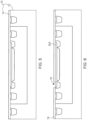
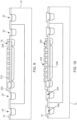
- Figures 5 to 10 show an exemplary method of forming the resistive filter stack 346 on the top surface of the first SPAD 306.
- the method starts at figure 5 .
- the basic SPAD structure (identified by the reference number 10), realised by implantation, annealing and etching processes, is already present. It includes a bulk 12 and a field oxide layer 14 covering the bulk 12.
- the single field oxide layer 14 may be replaced by a layer stack comprising several oxide and metal layers, preferably formed with a CMOS process.
- the first step is to etch a clearance 16 into the field oxide layer 14 to lay bare a section of the shallow extrinsic semiconductor layer 324.
- the result of this first step is shown in figure 6 .
- the next step is to form the resistive longpass filter 310. This is done by, first, the deposition of a polycrystalline silicon layer. This layer is then patterned to obtain an interdigitated stripe geometry. The result is shown in figure 7 .
- the next step is an etching step, which creates a clearance 18 in the intermediate dielectric layer 350.
- This clearance 18 uncovers the second end 358 of the longpass filter 310.
- further clearances 20 are etched into the field oxide layer 14 to provide access to the enrichment layers in the bulk 12. The result of this step is shown in figure 9 .
- the final step is a metallisation step.
- Metal for example, aluminium
- Metal is deposited on selected areas to obtain the cathode contact 334, the substrate contact 336, the resistor contact 352 and the set of masking strips 354. The result is shown in figure 10 .
- the metal layer 334, 336, 352 and 354 may be covered by a dielectric passivation layer (e.g. an oxide layer).
- a dielectric passivation layer e.g. an oxide layer
- the integrated photodetecting semiconductor optoelectronic component of the present disclosure may comprise one or more additional SPADs with one or more corresponding additional semiconductor optical longpass filters for measuring the intensity of one or more additional colour constituents of incident light.
- the additional longpass filters may have increasing cutoff wavelengths. This may be achieved by using absorbing layers of different thickness. The differential analysis may then be extended accordingly. Likewise, one would then also add one or more readout channels to the electronic circuitry.
Landscapes
- Physics & Mathematics (AREA)
- General Physics & Mathematics (AREA)
- Engineering & Computer Science (AREA)
- Computer Networks & Wireless Communication (AREA)
- Radar, Positioning & Navigation (AREA)
- Remote Sensing (AREA)
- Optics & Photonics (AREA)
- Spectroscopy & Molecular Physics (AREA)
- Health & Medical Sciences (AREA)
- Toxicology (AREA)
- Electromagnetism (AREA)
- Life Sciences & Earth Sciences (AREA)
- Sustainable Development (AREA)
- Photometry And Measurement Of Optical Pulse Characteristics (AREA)
- Optical Radar Systems And Details Thereof (AREA)
- Light Receiving Elements (AREA)
Claims (12)
- Composant optoélectronique semi-conducteur à photodétection intégrée (300) pour mesurer l'intensité (I1, I2) de chacun des deux constituants de couleur (C1, C2) de la lumière bichromatique (DL) irradiant le composant optoélectronique, le composant (300) comprenant :- un premier SPAD (306) adapté à la détection de photons sur une large gamme de longueurs d'onde, le premier SPAD comprenant une surface active (340) permettant aux photons à détecter de pénétrer dans le premier SPAD;- un second SPAD (308) adapté à la détection de photons sur une large gamme de longueurs d'onde, le second SPAD étant disposé à côté du premier SPAD (306);- un filtre optique semi-conducteur à longue portée (310) qui couvre au moins partiellement la surface active (340) du premier SPAD, le filtre à longue portée (310) étant permissif pour un premier (C1) des deux constituants de couleur de la lumière bichromatique (DL) et bloquant le second (C2) des deux constituants de couleur de la lumière bichromatique (DL);- un circuit électronique (304) pour la lecture et le traitement des signaux de détection (S1, S2) délivrés par le premier et le second SPAD, le circuit électronique étant adapté pour fournir:l'analyse différentielle effectuée par le circuit électronique (304) pour fournir le second signal de sortie d'intensité I2 comprend les étapes suivantes :i) un premier signal de sortie d'intensité I1 indiquant l'intensité du premier constituant coloré (C1), sur la base du signal de détection (S1) délivré par le premier SPAD; etii) un deuxième signal de sortie d'intensité I2 indiquant l'intensité du deuxième constituant de couleur (C2), par une analyse différentielle basée sur les signaux de détection (S1, S2) fournis par le premier et le deuxième SPAD;- déterminer un premier taux de détection de photons N1 à partir du signal de sortie (S1) délivré par le premier SPAD (306);- déterminer un second taux de détection de photons N2 à partir du signal de sortie (S2) délivré par le second SPAD (308); et- calculer le deuxième signal de sortie d'intensité I2 à l'aide de la formule suivante:

- Le composant (300) de la revendication 1, dans lequel le filtre à longue portée (310) est une couche unique de matériau semi-conducteur déposée au-dessus de la surface active (340) du premier SPAD.
- Le composant (300) de l'une des revendications précédentes, dans lequel le matériau semi-conducteur du filtre passe-haut (310) est du silicium, du germanium, de l'arséniure de gallium ou du nitrure de gallium.
- Le composant (300) de l'une des revendications précédentes, dans lequel le filtre passe long (310) se double d'un élément électrique fonctionnel faisant partie d'un circuit électrique.
- Le composant (300) de la revendication 4, dans lequel le matériau semi-conducteur du filtre passe-haut (310) est dopé de manière à ce que les propriétés électriques du matériau du filtre passe-haut soient adaptées à son rôle supplémentaire en tant qu'élément électrique fonctionnel.
- Le composant (300) de la revendication 4 ou de la revendication 5, dans lequel le filtre passe long (310) sert également de résistance passive d'extinction pour le premier SPAD (306).
- Le composant (300) de la revendication 6, dans lequel le filtre long (310) a la forme d'un chemin sinueux conducteur d'électricité qui forme la résistance passive d'extinction.
- Le composant (300) de la revendication 7, dans lequel la forme sinueuse du filtre passe-haut (310) définit un ensemble d'interstices non filtrants (359), et dans lequel lesdits interstices (359) sont couverts par un masque optique (354), de préférence en métal, qui est opaque à la lumière bichromatique (DL).
- Le composant (300) de l'une des revendications précédentes, dans lequel le circuit électronique (304) comprend un convertisseur temps-numérique (316) pour les mesures de temps de vol.
- Le composant (300) de l'une des revendications précédentes, dans lequel le premier SPAD (306) et le second SPAD (308) ont la même structure de jonction p-n.
- Le composant (300) de l'une des revendications précédentes, dans lequel les deux constituants de couleur (C1, C2) de la lumière bichromatique sont respectivement la lumière infrarouge proche et la lumière bleue ultraviolette proche.
- Le composant de l'une des revendications précédentes, comprenant en outre un ou plusieurs SPAD supplémentaires avec un ou plusieurs filtres optiques semi-conducteurs à longue passe correspondants pour mesurer l'intensité d'un ou plusieurs composants de couleur supplémentaires de la lumière incidente.
Applications Claiming Priority (2)
| Application Number | Priority Date | Filing Date | Title |
|---|---|---|---|
| DE102020201453 | 2020-02-06 | ||
| PCT/EP2021/052820 WO2021156447A1 (fr) | 2020-02-06 | 2021-02-05 | Élément optoélectronique semi-conducteur de photodétection intégré |
Publications (2)
| Publication Number | Publication Date |
|---|---|
| EP4100704A1 EP4100704A1 (fr) | 2022-12-14 |
| EP4100704B1 true EP4100704B1 (fr) | 2024-08-14 |
Family
ID=77199187
Family Applications (3)
| Application Number | Title | Priority Date | Filing Date |
|---|---|---|---|
| EP21703702.7A Active EP4100704B1 (fr) | 2020-02-06 | 2021-02-05 | Élément optoélectronique semi-conducteur de photodétection intégré |
| EP21704220.9A Pending EP4100705A1 (fr) | 2020-02-06 | 2021-02-05 | Capteur de lumière ambiante |
| EP21703701.9A Pending EP4100764A1 (fr) | 2020-02-06 | 2021-02-05 | Module de projection de pixel lumineux |
Family Applications After (2)
| Application Number | Title | Priority Date | Filing Date |
|---|---|---|---|
| EP21704220.9A Pending EP4100705A1 (fr) | 2020-02-06 | 2021-02-05 | Capteur de lumière ambiante |
| EP21703701.9A Pending EP4100764A1 (fr) | 2020-02-06 | 2021-02-05 | Module de projection de pixel lumineux |
Country Status (4)
| Country | Link |
|---|---|
| US (3) | US20230116903A1 (fr) |
| EP (3) | EP4100704B1 (fr) |
| CN (3) | CN115104013A (fr) |
| WO (3) | WO2021156446A1 (fr) |
Families Citing this family (1)
| Publication number | Priority date | Publication date | Assignee | Title |
|---|---|---|---|---|
| WO2026079610A1 (fr) * | 2024-10-10 | 2026-04-16 | 엘지이노텍 주식회사 | Structure de pixel spad intégrée comprenant une résistance structurée en méandres |
Family Cites Families (42)
| Publication number | Priority date | Publication date | Assignee | Title |
|---|---|---|---|---|
| IL106265A (en) * | 1992-07-13 | 1999-07-14 | Hughes Aircraft Co | Extrinsic semiconductor optical filter |
| US6359274B1 (en) * | 1999-01-25 | 2002-03-19 | Gentex Corporation | Photodiode light sensor |
| JP4623349B2 (ja) * | 2001-05-23 | 2011-02-02 | ソニー株式会社 | 薄膜型ndフィルタおよびその製造方法 |
| US20060199260A1 (en) * | 2002-05-01 | 2006-09-07 | Zhiyu Zhang | Microbioreactor for continuous cell culture |
| JP4595687B2 (ja) * | 2004-07-20 | 2010-12-08 | 住友金属鉱山株式会社 | 吸収型多層膜ndフィルター |
| WO2006037022A2 (fr) * | 2004-09-24 | 2006-04-06 | Massachusetts Institute Of Technology | Microbioreacteur de culture cellulaire continue |
| JP4613706B2 (ja) * | 2004-11-24 | 2011-01-19 | 住友金属鉱山株式会社 | 吸収型多層膜ndフィルター |
| US7430352B2 (en) * | 2005-07-29 | 2008-09-30 | Aculight Corporation | Multi-segment photonic-crystal-rod waveguides for amplification of high-power pulsed optical radiation and associated method |
| US20080176332A1 (en) * | 2006-09-29 | 2008-07-24 | The Regents Of The University Of California | Systems and methods for identifying and disrupting cellular organelles |
| JP2008098516A (ja) * | 2006-10-13 | 2008-04-24 | Sanyo Electric Co Ltd | 光電変換装置 |
| TW200832687A (en) * | 2007-01-30 | 2008-08-01 | Univ Nat Taiwan | Ambient light sensor |
| US7960807B2 (en) * | 2007-02-09 | 2011-06-14 | Intersil Americas Inc. | Ambient light detectors using conventional CMOS image sensor process |
| US9645010B2 (en) * | 2009-03-10 | 2017-05-09 | The Regents Of The University Of California | Fluidic flow cytometry devices and methods |
| JP2010238274A (ja) * | 2009-03-30 | 2010-10-21 | Sanyo Electric Co Ltd | 光ピックアップ装置 |
| US8492699B2 (en) * | 2009-09-22 | 2013-07-23 | Intersil Americas Inc. | Photodetectors useful as ambient light sensors having an optical filter rejecting a portion of infrared light |
| CN101799324A (zh) * | 2009-12-15 | 2010-08-11 | 杭州远方光电信息有限公司 | 一种亮度计 |
| JP2012021819A (ja) * | 2010-07-12 | 2012-02-02 | Panasonic Electric Works Co Ltd | 測光装置 |
| US20120313201A1 (en) * | 2011-06-13 | 2012-12-13 | Intersil Americas LLC | Optical sensor devices including front-end-of-line (feol) optical filters and methods for fabricating optical sensor devices |
| ITTO20110649A1 (it) * | 2011-07-19 | 2013-01-20 | St Microelectronics Srl | Dispositivo di fotorivelazione con copertura protettiva e antiriflesso, e relativo metodo di fabbricazione |
| GB2496399A (en) * | 2011-11-09 | 2013-05-15 | St Microelectronics Res & Dev | A sensor for range finding and ambient light measurement including a SPAD array |
| US9568362B2 (en) * | 2012-12-19 | 2017-02-14 | Viavi Solutions Inc. | Spectroscopic assembly and method |
| US9448346B2 (en) * | 2012-12-19 | 2016-09-20 | Viavi Solutions Inc. | Sensor device including one or more metal-dielectric optical filters |
| KR102129923B1 (ko) * | 2013-07-16 | 2020-07-03 | 엘지전자 주식회사 | 듀얼 스크린 상에 서로 다른 영상 투사가 가능한 디스플레이 장치 |
| US9140971B2 (en) * | 2013-10-31 | 2015-09-22 | Microvision, Inc. | Scanning laser proximity detection |
| EP2887771B1 (fr) * | 2013-12-20 | 2018-02-28 | ams AG | Agencement de capteurs pour commander l'éclairage d'une pièce, réseau de capteurs pour commander l'éclairage de pièce et procédé pour commander un éclairage ambiant |
| US9627424B2 (en) * | 2014-11-19 | 2017-04-18 | Silicon Laboratories Inc. | Photodiodes for ambient light sensing and proximity sensing |
| US9608027B2 (en) | 2015-02-17 | 2017-03-28 | Omnivision Technologies, Inc. | Stacked embedded SPAD image sensor for attached 3D information |
| WO2016161392A1 (fr) * | 2015-04-01 | 2016-10-06 | Massachusetts Institute Of Technology | Dispositifs optoélectroniques fabriqués avec des semi-conducteurs tolérants aux défauts |
| CN108449956A (zh) | 2015-11-30 | 2018-08-24 | Jsr株式会社 | 光学滤波器、环境光传感器及传感器模块 |
| US10962764B2 (en) * | 2016-04-01 | 2021-03-30 | Intel Corporation | Laser projector and camera |
| US9955090B2 (en) | 2016-07-20 | 2018-04-24 | Omnivision Technologies, Inc. | High dynamic range image sensor with virtual high-low sensitivity pixels |
| US11303859B2 (en) * | 2016-09-29 | 2022-04-12 | Stmicroelectronics (Research & Development) Limited | Time of flight sensing for brightness and autofocus control in image projection devices |
| DE102016124004A1 (de) * | 2016-12-09 | 2018-06-14 | Leica Microsystems Cms Gmbh | Optisches Gerät mit mindestens einem spektral selektiven Bauelement |
| US10312275B2 (en) * | 2017-04-25 | 2019-06-04 | Semiconductor Components Industries, Llc | Single-photon avalanche diode image sensor with photon counting and time-of-flight detection capabilities |
| IT201700053528A1 (it) * | 2017-05-17 | 2018-11-17 | St Microelectronics Srl | Dispositivo optoelettronico accordabile e sensore di pressione sanguigna includente il medesimo |
| US11639896B2 (en) * | 2017-07-14 | 2023-05-02 | King Abdullah University Of Science And Technology | Size controllable conjugated polymer nanoparticles with fluorescence in the spectral range between far-red and short-wavelength infrared |
| CN108414083B (zh) * | 2018-02-27 | 2019-08-30 | 商洛学院 | 一种可人眼透射率修正的多功能照度传感器及设计方法 |
| US10901089B2 (en) * | 2018-03-26 | 2021-01-26 | Huawei Technologies Co., Ltd. | Coherent LIDAR method and apparatus |
| US10613341B2 (en) | 2018-04-09 | 2020-04-07 | Microvision, Inc. | Method and apparatus for laser beam combining and speckle reduction |
| US10447951B1 (en) * | 2018-04-11 | 2019-10-15 | Qualcomm Incorporated | Dynamic range estimation with fast and slow sensor pixels |
| CN112771410A (zh) * | 2018-08-16 | 2021-05-07 | 感觉光子公司 | 集成激光雷达图像传感器设备和系统以及相关的操作方法 |
| WO2021213674A1 (fr) * | 2020-04-24 | 2021-10-28 | Osram Opto Semiconductors Gmbh | Photodiode et procédé de fonctionnement d'une photodiode |
-
2021
- 2021-02-05 WO PCT/EP2021/052819 patent/WO2021156446A1/fr not_active Ceased
- 2021-02-05 US US17/797,906 patent/US20230116903A1/en active Pending
- 2021-02-05 CN CN202180013382.XA patent/CN115104013A/zh active Pending
- 2021-02-05 EP EP21703702.7A patent/EP4100704B1/fr active Active
- 2021-02-05 US US17/797,882 patent/US12484336B2/en active Active
- 2021-02-05 CN CN202180012845.0A patent/CN115053148B/zh active Active
- 2021-02-05 WO PCT/EP2021/052820 patent/WO2021156447A1/fr not_active Ceased
- 2021-02-05 US US17/798,059 patent/US12289930B2/en active Active
- 2021-02-05 EP EP21704220.9A patent/EP4100705A1/fr active Pending
- 2021-02-05 EP EP21703701.9A patent/EP4100764A1/fr active Pending
- 2021-02-05 CN CN202180013294.XA patent/CN115104012B/zh active Active
- 2021-02-05 WO PCT/EP2021/052818 patent/WO2021156445A1/fr not_active Ceased
Also Published As
| Publication number | Publication date |
|---|---|
| WO2021156445A1 (fr) | 2021-08-12 |
| CN115104012B (zh) | 2025-08-12 |
| US12289930B2 (en) | 2025-04-29 |
| CN115104013A (zh) | 2022-09-23 |
| WO2021156447A1 (fr) | 2021-08-12 |
| CN115053148A (zh) | 2022-09-13 |
| CN115104012A (zh) | 2022-09-23 |
| US12484336B2 (en) | 2025-11-25 |
| US20230116903A1 (en) | 2023-04-13 |
| EP4100705A1 (fr) | 2022-12-14 |
| EP4100764A1 (fr) | 2022-12-14 |
| EP4100704A1 (fr) | 2022-12-14 |
| CN115053148B (zh) | 2024-11-12 |
| US20230062921A1 (en) | 2023-03-02 |
| WO2021156446A1 (fr) | 2021-08-12 |
| US20230084888A1 (en) | 2023-03-16 |
Similar Documents
| Publication | Publication Date | Title |
|---|---|---|
| US8461533B2 (en) | Radiation sensor | |
| EP2731148B1 (fr) | Réseau de photodiodes, procédé de détermination de tension de référence et procédé de détermination de tension de fonctionnement recommandée | |
| US9978802B2 (en) | Multiband optoelectronic device for colorimetric applications and related manufacturing process | |
| CN107665886A (zh) | 用于检测红外线辐射的盖革模式雪崩光电二极管阵列 | |
| US20120133799A1 (en) | Radiation sensor | |
| US9379158B2 (en) | Optical detector unit | |
| US12345569B2 (en) | SPAD-based photodetectors | |
| US20130214134A1 (en) | Photon detector | |
| CN105405914A (zh) | 具有滤光器的紫外传感器 | |
| JPH01207640A (ja) | 半導体光検出装置と紫外線検出方法および半導体光検出素子とその製造方法 | |
| EP4100704B1 (fr) | Élément optoélectronique semi-conducteur de photodétection intégré | |
| EP2643667A1 (fr) | Détecteur de rayonnement | |
| US20150285942A1 (en) | Solid state photo multiplier device | |
| EP3229278B1 (fr) | Dispositif de détection et procédé de fabrication associé | |
| EP3404379A1 (fr) | Dispositif optique pour mesures d'angle | |
| Saveliev | Silicon photomultiplier-new era of photon detection | |
| US20060231913A1 (en) | Method for determining wavelengths of light incident on a stacked photodetector structure | |
| US11888078B2 (en) | Light detection with semiconductor photodiodes | |
| JPH0517492B2 (fr) | ||
| Polzer et al. | Wavelength detection with integrated filter-less BiCMOS RGB sensor | |
| WO2021213674A1 (fr) | Photodiode et procédé de fonctionnement d'une photodiode | |
| EP2347444B1 (fr) | Détecteur de rayonnement électromagnétique à sélection de longueur d onde utilisant des pores en qualité de cristal photonique | |
| KR20260050318A (ko) | 단일 광자 애벌런치 포토다이오드 소자 및 그 제조 방법 | |
| RU2501116C1 (ru) | Способ измерения диффузионной длины неосновных носителей заряда в полупроводниках и тестовая структура для его осуществления | |
| Batistell et al. | Color Sensor for Ambient Light Measurements in 130 nm CMOS Technology |
Legal Events
| Date | Code | Title | Description |
|---|---|---|---|
| STAA | Information on the status of an ep patent application or granted ep patent |
Free format text: STATUS: UNKNOWN |
|
| STAA | Information on the status of an ep patent application or granted ep patent |
Free format text: STATUS: THE INTERNATIONAL PUBLICATION HAS BEEN MADE |
|
| PUAI | Public reference made under article 153(3) epc to a published international application that has entered the european phase |
Free format text: ORIGINAL CODE: 0009012 |
|
| STAA | Information on the status of an ep patent application or granted ep patent |
Free format text: STATUS: REQUEST FOR EXAMINATION WAS MADE |
|
| 17P | Request for examination filed |
Effective date: 20220905 |
|
| AK | Designated contracting states |
Kind code of ref document: A1 Designated state(s): AL AT BE BG CH CY CZ DE DK EE ES FI FR GB GR HR HU IE IS IT LI LT LU LV MC MK MT NL NO PL PT RO RS SE SI SK SM TR |
|
| DAV | Request for validation of the european patent (deleted) | ||
| DAX | Request for extension of the european patent (deleted) | ||
| P01 | Opt-out of the competence of the unified patent court (upc) registered |
Effective date: 20230613 |
|
| GRAP | Despatch of communication of intention to grant a patent |
Free format text: ORIGINAL CODE: EPIDOSNIGR1 |
|
| STAA | Information on the status of an ep patent application or granted ep patent |
Free format text: STATUS: GRANT OF PATENT IS INTENDED |
|
| INTG | Intention to grant announced |
Effective date: 20240307 |
|
| RIC1 | Information provided on ipc code assigned before grant |
Ipc: G02B 5/20 20060101ALI20240223BHEP Ipc: H01L 31/0232 20140101ALI20240223BHEP Ipc: G01J 1/44 20060101ALI20240223BHEP Ipc: H01L 31/0216 20140101ALI20240223BHEP Ipc: H01L 31/107 20060101ALI20240223BHEP Ipc: G01J 1/04 20060101ALI20240223BHEP Ipc: G01J 1/42 20060101AFI20240223BHEP |
|
| GRAS | Grant fee paid |
Free format text: ORIGINAL CODE: EPIDOSNIGR3 |
|
| GRAA | (expected) grant |
Free format text: ORIGINAL CODE: 0009210 |
|
| STAA | Information on the status of an ep patent application or granted ep patent |
Free format text: STATUS: THE PATENT HAS BEEN GRANTED |
|
| AK | Designated contracting states |
Kind code of ref document: B1 Designated state(s): AL AT BE BG CH CY CZ DE DK EE ES FI FR GB GR HR HU IE IS IT LI LT LU LV MC MK MT NL NO PL PT RO RS SE SI SK SM TR |
|
| REG | Reference to a national code |
Ref country code: GB Ref legal event code: FG4D |
|
| REG | Reference to a national code |
Ref country code: CH Ref legal event code: EP |
|
| REG | Reference to a national code |
Ref country code: DE Ref legal event code: R096 Ref document number: 602021017190 Country of ref document: DE |
|
| REG | Reference to a national code |
Ref country code: IE Ref legal event code: FG4D |
|
| REG | Reference to a national code |
Ref country code: LT Ref legal event code: MG9D |
|
| REG | Reference to a national code |
Ref country code: DE Ref legal event code: R082 Ref document number: 602021017190 Country of ref document: DE Representative=s name: IMPULS LEGAL PARTG MBB, DE |
|
| REG | Reference to a national code |
Ref country code: NL Ref legal event code: MP Effective date: 20240814 |
|
| PG25 | Lapsed in a contracting state [announced via postgrant information from national office to epo] |
Ref country code: NO Free format text: LAPSE BECAUSE OF FAILURE TO SUBMIT A TRANSLATION OF THE DESCRIPTION OR TO PAY THE FEE WITHIN THE PRESCRIBED TIME-LIMIT Effective date: 20241114 |
|
| REG | Reference to a national code |
Ref country code: AT Ref legal event code: MK05 Ref document number: 1713673 Country of ref document: AT Kind code of ref document: T Effective date: 20240814 |
|
| PG25 | Lapsed in a contracting state [announced via postgrant information from national office to epo] |
Ref country code: PT Free format text: LAPSE BECAUSE OF FAILURE TO SUBMIT A TRANSLATION OF THE DESCRIPTION OR TO PAY THE FEE WITHIN THE PRESCRIBED TIME-LIMIT Effective date: 20241216 Ref country code: NL Free format text: LAPSE BECAUSE OF FAILURE TO SUBMIT A TRANSLATION OF THE DESCRIPTION OR TO PAY THE FEE WITHIN THE PRESCRIBED TIME-LIMIT Effective date: 20240814 Ref country code: PL Free format text: LAPSE BECAUSE OF FAILURE TO SUBMIT A TRANSLATION OF THE DESCRIPTION OR TO PAY THE FEE WITHIN THE PRESCRIBED TIME-LIMIT Effective date: 20240814 Ref country code: GR Free format text: LAPSE BECAUSE OF FAILURE TO SUBMIT A TRANSLATION OF THE DESCRIPTION OR TO PAY THE FEE WITHIN THE PRESCRIBED TIME-LIMIT Effective date: 20241115 Ref country code: FI Free format text: LAPSE BECAUSE OF FAILURE TO SUBMIT A TRANSLATION OF THE DESCRIPTION OR TO PAY THE FEE WITHIN THE PRESCRIBED TIME-LIMIT Effective date: 20240814 |
|
| PG25 | Lapsed in a contracting state [announced via postgrant information from national office to epo] |
Ref country code: BG Free format text: LAPSE BECAUSE OF FAILURE TO SUBMIT A TRANSLATION OF THE DESCRIPTION OR TO PAY THE FEE WITHIN THE PRESCRIBED TIME-LIMIT Effective date: 20240814 |
|
| PG25 | Lapsed in a contracting state [announced via postgrant information from national office to epo] |
Ref country code: LV Free format text: LAPSE BECAUSE OF FAILURE TO SUBMIT A TRANSLATION OF THE DESCRIPTION OR TO PAY THE FEE WITHIN THE PRESCRIBED TIME-LIMIT Effective date: 20240814 |
|
| PG25 | Lapsed in a contracting state [announced via postgrant information from national office to epo] |
Ref country code: AT Free format text: LAPSE BECAUSE OF FAILURE TO SUBMIT A TRANSLATION OF THE DESCRIPTION OR TO PAY THE FEE WITHIN THE PRESCRIBED TIME-LIMIT Effective date: 20240814 Ref country code: IS Free format text: LAPSE BECAUSE OF FAILURE TO SUBMIT A TRANSLATION OF THE DESCRIPTION OR TO PAY THE FEE WITHIN THE PRESCRIBED TIME-LIMIT Effective date: 20241214 |
|
| PG25 | Lapsed in a contracting state [announced via postgrant information from national office to epo] |
Ref country code: HR Free format text: LAPSE BECAUSE OF FAILURE TO SUBMIT A TRANSLATION OF THE DESCRIPTION OR TO PAY THE FEE WITHIN THE PRESCRIBED TIME-LIMIT Effective date: 20240814 |
|
| PG25 | Lapsed in a contracting state [announced via postgrant information from national office to epo] |
Ref country code: RS Free format text: LAPSE BECAUSE OF FAILURE TO SUBMIT A TRANSLATION OF THE DESCRIPTION OR TO PAY THE FEE WITHIN THE PRESCRIBED TIME-LIMIT Effective date: 20241114 Ref country code: ES Free format text: LAPSE BECAUSE OF FAILURE TO SUBMIT A TRANSLATION OF THE DESCRIPTION OR TO PAY THE FEE WITHIN THE PRESCRIBED TIME-LIMIT Effective date: 20240814 |
|
| PG25 | Lapsed in a contracting state [announced via postgrant information from national office to epo] |
Ref country code: RS Free format text: LAPSE BECAUSE OF FAILURE TO SUBMIT A TRANSLATION OF THE DESCRIPTION OR TO PAY THE FEE WITHIN THE PRESCRIBED TIME-LIMIT Effective date: 20241114 Ref country code: PT Free format text: LAPSE BECAUSE OF FAILURE TO SUBMIT A TRANSLATION OF THE DESCRIPTION OR TO PAY THE FEE WITHIN THE PRESCRIBED TIME-LIMIT Effective date: 20241216 Ref country code: PL Free format text: LAPSE BECAUSE OF FAILURE TO SUBMIT A TRANSLATION OF THE DESCRIPTION OR TO PAY THE FEE WITHIN THE PRESCRIBED TIME-LIMIT Effective date: 20240814 Ref country code: NO Free format text: LAPSE BECAUSE OF FAILURE TO SUBMIT A TRANSLATION OF THE DESCRIPTION OR TO PAY THE FEE WITHIN THE PRESCRIBED TIME-LIMIT Effective date: 20241114 Ref country code: NL Free format text: LAPSE BECAUSE OF FAILURE TO SUBMIT A TRANSLATION OF THE DESCRIPTION OR TO PAY THE FEE WITHIN THE PRESCRIBED TIME-LIMIT Effective date: 20240814 Ref country code: LV Free format text: LAPSE BECAUSE OF FAILURE TO SUBMIT A TRANSLATION OF THE DESCRIPTION OR TO PAY THE FEE WITHIN THE PRESCRIBED TIME-LIMIT Effective date: 20240814 Ref country code: IS Free format text: LAPSE BECAUSE OF FAILURE TO SUBMIT A TRANSLATION OF THE DESCRIPTION OR TO PAY THE FEE WITHIN THE PRESCRIBED TIME-LIMIT Effective date: 20241214 Ref country code: HR Free format text: LAPSE BECAUSE OF FAILURE TO SUBMIT A TRANSLATION OF THE DESCRIPTION OR TO PAY THE FEE WITHIN THE PRESCRIBED TIME-LIMIT Effective date: 20240814 Ref country code: GR Free format text: LAPSE BECAUSE OF FAILURE TO SUBMIT A TRANSLATION OF THE DESCRIPTION OR TO PAY THE FEE WITHIN THE PRESCRIBED TIME-LIMIT Effective date: 20241115 Ref country code: FI Free format text: LAPSE BECAUSE OF FAILURE TO SUBMIT A TRANSLATION OF THE DESCRIPTION OR TO PAY THE FEE WITHIN THE PRESCRIBED TIME-LIMIT Effective date: 20240814 Ref country code: ES Free format text: LAPSE BECAUSE OF FAILURE TO SUBMIT A TRANSLATION OF THE DESCRIPTION OR TO PAY THE FEE WITHIN THE PRESCRIBED TIME-LIMIT Effective date: 20240814 Ref country code: BG Free format text: LAPSE BECAUSE OF FAILURE TO SUBMIT A TRANSLATION OF THE DESCRIPTION OR TO PAY THE FEE WITHIN THE PRESCRIBED TIME-LIMIT Effective date: 20240814 Ref country code: AT Free format text: LAPSE BECAUSE OF FAILURE TO SUBMIT A TRANSLATION OF THE DESCRIPTION OR TO PAY THE FEE WITHIN THE PRESCRIBED TIME-LIMIT Effective date: 20240814 |
|
| PG25 | Lapsed in a contracting state [announced via postgrant information from national office to epo] |
Ref country code: DK Free format text: LAPSE BECAUSE OF FAILURE TO SUBMIT A TRANSLATION OF THE DESCRIPTION OR TO PAY THE FEE WITHIN THE PRESCRIBED TIME-LIMIT Effective date: 20240814 Ref country code: RO Free format text: LAPSE BECAUSE OF FAILURE TO SUBMIT A TRANSLATION OF THE DESCRIPTION OR TO PAY THE FEE WITHIN THE PRESCRIBED TIME-LIMIT Effective date: 20240814 Ref country code: SM Free format text: LAPSE BECAUSE OF FAILURE TO SUBMIT A TRANSLATION OF THE DESCRIPTION OR TO PAY THE FEE WITHIN THE PRESCRIBED TIME-LIMIT Effective date: 20240814 |
|
| PG25 | Lapsed in a contracting state [announced via postgrant information from national office to epo] |
Ref country code: EE Free format text: LAPSE BECAUSE OF FAILURE TO SUBMIT A TRANSLATION OF THE DESCRIPTION OR TO PAY THE FEE WITHIN THE PRESCRIBED TIME-LIMIT Effective date: 20240814 |
|
| PG25 | Lapsed in a contracting state [announced via postgrant information from national office to epo] |
Ref country code: CZ Free format text: LAPSE BECAUSE OF FAILURE TO SUBMIT A TRANSLATION OF THE DESCRIPTION OR TO PAY THE FEE WITHIN THE PRESCRIBED TIME-LIMIT Effective date: 20240814 |
|
| PG25 | Lapsed in a contracting state [announced via postgrant information from national office to epo] |
Ref country code: SK Free format text: LAPSE BECAUSE OF FAILURE TO SUBMIT A TRANSLATION OF THE DESCRIPTION OR TO PAY THE FEE WITHIN THE PRESCRIBED TIME-LIMIT Effective date: 20240814 Ref country code: IT Free format text: LAPSE BECAUSE OF FAILURE TO SUBMIT A TRANSLATION OF THE DESCRIPTION OR TO PAY THE FEE WITHIN THE PRESCRIBED TIME-LIMIT Effective date: 20240814 |
|
| REG | Reference to a national code |
Ref country code: DE Ref legal event code: R097 Ref document number: 602021017190 Country of ref document: DE |
|
| PLBE | No opposition filed within time limit |
Free format text: ORIGINAL CODE: 0009261 |
|
| STAA | Information on the status of an ep patent application or granted ep patent |
Free format text: STATUS: NO OPPOSITION FILED WITHIN TIME LIMIT |
|
| 26N | No opposition filed |
Effective date: 20250515 |
|
| PG25 | Lapsed in a contracting state [announced via postgrant information from national office to epo] |
Ref country code: SE Free format text: LAPSE BECAUSE OF FAILURE TO SUBMIT A TRANSLATION OF THE DESCRIPTION OR TO PAY THE FEE WITHIN THE PRESCRIBED TIME-LIMIT Effective date: 20240814 |
|
| PG25 | Lapsed in a contracting state [announced via postgrant information from national office to epo] |
Ref country code: MC Free format text: LAPSE BECAUSE OF FAILURE TO SUBMIT A TRANSLATION OF THE DESCRIPTION OR TO PAY THE FEE WITHIN THE PRESCRIBED TIME-LIMIT Effective date: 20240814 |
|
| REG | Reference to a national code |
Ref country code: CH Ref legal event code: PL |
|
| PG25 | Lapsed in a contracting state [announced via postgrant information from national office to epo] |
Ref country code: LU Free format text: LAPSE BECAUSE OF NON-PAYMENT OF DUE FEES Effective date: 20250205 |
|
| PG25 | Lapsed in a contracting state [announced via postgrant information from national office to epo] |
Ref country code: CH Free format text: LAPSE BECAUSE OF NON-PAYMENT OF DUE FEES Effective date: 20250228 |
|
| GBPC | Gb: european patent ceased through non-payment of renewal fee |
Effective date: 20250205 |
|
| REG | Reference to a national code |
Ref country code: BE Ref legal event code: MM Effective date: 20250228 |
|
| PG25 | Lapsed in a contracting state [announced via postgrant information from national office to epo] |
Ref country code: GB Free format text: LAPSE BECAUSE OF NON-PAYMENT OF DUE FEES Effective date: 20250205 |
|
| PG25 | Lapsed in a contracting state [announced via postgrant information from national office to epo] |
Ref country code: FR Free format text: LAPSE BECAUSE OF NON-PAYMENT OF DUE FEES Effective date: 20250228 |
|
| PG25 | Lapsed in a contracting state [announced via postgrant information from national office to epo] |
Ref country code: BE Free format text: LAPSE BECAUSE OF NON-PAYMENT OF DUE FEES Effective date: 20250228 |
|
| PG25 | Lapsed in a contracting state [announced via postgrant information from national office to epo] |
Ref country code: IE Free format text: LAPSE BECAUSE OF NON-PAYMENT OF DUE FEES Effective date: 20250205 |
|
| PGFP | Annual fee paid to national office [announced via postgrant information from national office to epo] |
Ref country code: DE Payment date: 20260218 Year of fee payment: 6 |