EP4101006B1 - Vorrichtung mit einem satz von josephson-übergängen, system mit einer solchen vorrichtung und verfahren zur verwendung einer solchen vorrichtung - Google Patents
Vorrichtung mit einem satz von josephson-übergängen, system mit einer solchen vorrichtung und verfahren zur verwendung einer solchen vorrichtung Download PDFInfo
- Publication number
- EP4101006B1 EP4101006B1 EP21702681.4A EP21702681A EP4101006B1 EP 4101006 B1 EP4101006 B1 EP 4101006B1 EP 21702681 A EP21702681 A EP 21702681A EP 4101006 B1 EP4101006 B1 EP 4101006B1
- Authority
- EP
- European Patent Office
- Prior art keywords
- junction
- conductors
- portions
- configuration
- junctions
- Prior art date
- Legal status (The legal status is an assumption and is not a legal conclusion. Google has not performed a legal analysis and makes no representation as to the accuracy of the status listed.)
- Active
Links
Images




Classifications
-
- H—ELECTRICITY
- H01—ELECTRIC ELEMENTS
- H01Q—ANTENNAS, i.e. RADIO AERIALS
- H01Q1/00—Details of, or arrangements associated with, antennas
- H01Q1/36—Structural form of radiating elements, e.g. cone, spiral, umbrella; Particular materials used therewith
- H01Q1/364—Structural form of radiating elements, e.g. cone, spiral, umbrella; Particular materials used therewith using a particular conducting material, e.g. superconductor
-
- H—ELECTRICITY
- H10—SEMICONDUCTOR DEVICES; ELECTRIC SOLID-STATE DEVICES NOT OTHERWISE PROVIDED FOR
- H10N—ELECTRIC SOLID-STATE DEVICES NOT OTHERWISE PROVIDED FOR
- H10N69/00—Integrated devices, or assemblies of multiple devices, comprising at least one superconducting element covered by group H10N60/00
-
- G—PHYSICS
- G01—MEASURING; TESTING
- G01R—MEASURING ELECTRIC VARIABLES; MEASURING MAGNETIC VARIABLES
- G01R33/00—Arrangements or instruments for measuring magnetic variables
- G01R33/02—Measuring direction or magnitude of magnetic fields or magnetic flux
- G01R33/035—Measuring direction or magnitude of magnetic fields or magnetic flux using superconductive devices
- G01R33/0354—SQUIDS
-
- H—ELECTRICITY
- H10—SEMICONDUCTOR DEVICES; ELECTRIC SOLID-STATE DEVICES NOT OTHERWISE PROVIDED FOR
- H10N—ELECTRIC SOLID-STATE DEVICES NOT OTHERWISE PROVIDED FOR
- H10N60/00—Superconducting devices
- H10N60/10—Junction-based devices
- H10N60/12—Josephson-effect devices
-
- H—ELECTRICITY
- H10—SEMICONDUCTOR DEVICES; ELECTRIC SOLID-STATE DEVICES NOT OTHERWISE PROVIDED FOR
- H10N—ELECTRIC SOLID-STATE DEVICES NOT OTHERWISE PROVIDED FOR
- H10N60/00—Superconducting devices
- H10N60/10—Junction-based devices
- H10N60/128—Junction-based devices having three or more electrodes, e.g. transistor-like structures
-
- G—PHYSICS
- G06—COMPUTING OR CALCULATING; COUNTING
- G06N—COMPUTING ARRANGEMENTS BASED ON SPECIFIC COMPUTATIONAL MODELS
- G06N3/00—Computing arrangements based on biological models
- G06N3/02—Neural networks
- G06N3/06—Physical realisation, i.e. hardware implementation of neural networks, neurons or parts of neurons
- G06N3/063—Physical realisation, i.e. hardware implementation of neural networks, neurons or parts of neurons using electronic means
- G06N3/065—Analogue means
Definitions
- the present invention relates to a device comprising a set of Josephson junctions.
- the present invention also relates to a system comprising such a device as well as a method of using such a device.
- Josephson junctions comprising superconducting materials are a component of many electronic devices.
- Superconductivity is the particularity, for certain so-called superconducting materials, of having zero electrical resistance when their temperature is below a temperature called critical temperature.
- Superconductivity is caused by the formation, in the material, of Cooper pairs made up of two electrons.
- a Josephson junction is formed by two superconductors separated by a non-superconducting barrier.
- the barrier is sufficiently thin so that the Cooper pairs can cross it, and therefore transit from one superconductor to another, by tunneling if the barrier layer is electrically insulating, or by classical electronic transport otherwise.
- the wave function of the Cooper pairs of the first superconductor extends through the barrier, into the second superconductor where it interferes with the wave function of the Cooper pairs of the second superconductor .
- the voltage V across a Josephson junction, and the intensity I of a current crossing the junction, are a function in particular of a critical current characteristic of the junction considered.
- This critical current is also a function of the component of the magnetic field in a plane transverse to the direction of stacking of the layers of the Josephson junction.
- a SQUID is formed by a superconducting loop comprising two Josephson junctions arranged in parallel.
- the electric currents circulating in the loop are impacted by any magnetic field passing through the loop, so that the value of the voltage between the two sides of each junction is modified.
- the value of the field local magnetic field is modified.
- SQIFs from the English “Superconducting Quantum Interference Filters”
- the voltage across the SQUIDs is a sinusoidal function of the value of the magnetic field, which makes the analysis of this voltage complex, and requires the use of specific devices.
- the responses of the individual SQUIDs tend to compensate each other beyond a given magnetic field value, but below this value the variation of the voltage as a function of the field is monotonous.
- the analysis of the voltage is therefore very simple over a range of magnetic fields centered on the zero value.
- a device comprising a substrate, a set of electrical conductors carried by one face of the substrate, a set of junctions carried by said face of the substrate and a set of control members, each electrical conductor being made in a superconducting material, each electrical conductor comprising a single first portion extending in a first direction tangential to the substrate and a set of second portions, the first portions of the electrical conductors being offset successively relative to each other in a second direction perpendicular to the first direction, at least three junctions being interposed in the second direction between each pair of first successive portions, each junction being connected to the first portion of each of the conductors between which the junction is interposed by a second portion of said conductor, each member of control being associated with a single junction among the set of junctions, and being configured to switch the associated junction between a first configuration in which the junction forms a Josephson junction between the conductors to which the junction is connected and a second configuration in which the junction prevents the passage of Cooper pairs between said drivers.
- a system comprising a control module and a device as previously described, the system being in particular an antenna.
- a method of using a device comprising a substrate, a set of electrical conductors carried by the substrate, a set of junctions and a set of control members, each electrical conductor being made of a superconducting material, is also proposed.
- each electrical conductor comprising a single first portion extending in a first direction tangential to the substrate and a set of second portions, the first portions of the electrical conductors being offset successively relative to each other in a second direction perpendicular to the first direction, at least three junctions being interposed in the second direction between each pair of first successive portions, each junction being connected to the first portion of each of the conductors between which the junction is interposed by a second portion of said conductor, the method comprising a switching step at least one junction between a first configuration in which the junction forms a Josephson junction between the conductors to which the junction is connected and a second configuration in which the junction prevents the passage of Cooper pairs between said conductors.
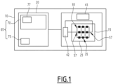
- a first example of system 10 is represented schematically on the figure 1 .
- the system 10 is, for example, a radio frequency transmission system such as an antenna.
- the system 10 is capable of transmitting and/or receiving, in particular receiving, electromagnetic waves having a frequency between zero and 4 TeraHertz (THz).
- THz TeraHertz
- the system 10 is an amplifier, in particular a low noise amplifier, a magnetic field sensor, an analog-digital converter, or even a filter.
- the system 10 comprises a device 15 and a control module 20.
- the device 15 comprises a substrate 25, a set of electrical conductors 30A, 30B, a set of junctions 35, a set of control members 40, a power supply 42 and a sensor 43.
- the electrical conductors 30A, 30B and the junctions 35 are capable of forming a SQIF comprising a set of SQUIDs connected to each other, in particular a two-dimensional network of SQUIDs.
- each SQUID is formed by portions of conductors 30A, 30B forming a superconducting loop and by two junctions 35 separating the loop into two portions connected to each other by the junctions 35.
- the two junctions 35 are connected in parallel between the two conductors 30A, 30B.
- the substrate 25 is designed to support each electrical conductor 30A, 30B, each junction 35 and each control member 40.
- the substrate 25 is made of an electrically insulating material such as sapphire or magnesium oxide MgO.
- the substrate 25 has a support face 45.
- the support face 45 is planar.
- a normal direction Z is defined for the substrate 25, perpendicular to the support face 45.
- a first direction X and a second direction Y are also defined. The first direction X and the second direction Y are perpendicular to each other. the other, and perpendicular to the normal direction Z.
- the number of conductors 30A, 30B is greater than or equal to two. According to the example shown schematically on the figure 2 , the device 15 comprises five conductors 30A, 30B. However, it should be noted that the number of conductors 30A, 30B is likely to vary, in particular to be greater than or equal to 10, in particular to be greater than or equal to 100.
- the set of conductors 30A, 30B comprises two end conductors 30A and at least one conductor 30B, in particular a plurality of conductors 30B, interposed between the two end conductors 30A in the second direction Y.
- the conductors 30B are in particular offset successively in relation to each other in the second direction Y.
- Two conductors 30A, 30B are said to be “successive” or “neighboring” if no other conductor 30A, 30B is interposed between the two conductors considered in the second direction Y.
- Conductors 30A, 30B are electrically connected in series.
- the set of conductors 30A, 30B is configured so that an electric current passes successively through one of the end conductors 30A, each conductor 30B then the other end conductor 30A.
- Each conductor 30A, 30B comprises a single first portion 50 and a set of second portions 55.
- Each end conductor 30A is electrically connected to a first electrode 57.
- the conductors 30A, 30B are, in particular, interposed in the second direction Y between the two first electrodes 57.
- Each conductor 30A, 30B is made of a first material M1.
- the first material M1 is a superconducting material.
- the first material M1 has a first resistivity R1, dependent on the temperature.
- the resistivity of a material is defined as the electrical resistance of a section of material 1 meter (m) long and 1 m 2 in section. Resistivity is generally expressed in ohm ⁇ meter ( ⁇ m).
- the electrical resistance measured between two contacts is defined as the ratio between the voltage measured across the two contacts and the electric current flowing in a circuit branch passing through the two terminals.
- the first material M1 has a first critical temperature Tc1.
- Tc1 first critical temperature
- the first critical temperature Tc1 is, in particular, less than or equal to a set temperature Tc at which the device 15 is intended to be used.
- the concentration of charge carriers is defined as being the sum of the electric charges of each charge carrier per unit volume of first material M1.
- the first material M1 is, for example, a material from the cuprate family.
- Cuprates are chemical compounds containing copper cations. Many compounds in the cuprate family exhibit the properties described above.
- the first material M1 is a mixed oxide of barium, copper, and yttrium.
- Mixed oxides of barium, copper and yttrium also denoted YBCO, are crystalline chemical compounds frequently having the chemical formula YBa 2 Cu 3 O 7- ⁇ , in which ⁇ is a real number greater than or equal to zero.
- ⁇ is between 0 and 0.6.
- the first material M1 is, for example, NdBaCuO or LaBaCuO.
- first materials M1 are possible, for example Nb or NbSn.
- the first portion 50 of each conductor 30A, 30B is carried by the support face 45.
- the first portion 50 extends, for example, in a direction tangential to the substrate 25, that is to say in a direction perpendicular to the normal direction Z. According to the example shown in the figure 2 , the first portion 50 of each conductor 30A, 30B extends in the first direction X.
- Each first portion 50 is, for example, rectilinear.
- the first portion has a curved shape in a plane perpendicular to the normal direction Z, for example a sinusoidal shape around a straight line segment parallel to the first direction X.
- Each first portion 50 is, for example, a portion of a layer of the first material M1 carried by the support face 45.
- each first portion 50 has a thickness, measured in the normal direction Z, of between 30 nanometers (nm) and 200 nm.
- a width of the first portion 50, measured for example along the second direction Y, is between 100 nm and 2 micrometers ( ⁇ m).
- the first portions 50 of the conductors 30A, 30B are offset successively in the second direction Y relative to each other.
- each first portion 50 extends along a proper line, the proper lines being parallel to each other.
- the first portions 50 of the conductors 30A, 30B are not offset relative to each other in the first direction 'other according to the first direction X are also possible.
- a distance between the clean lines of two first successive portions 50 is, for example, between 300 nm and 10 ⁇ m. According to one embodiment, this distance is uniform. In other words, this distance is equal for each pair of two first portions 50 belonging to two successive conductors 30.
- Each first portion 50 is distinct from the other first portions 50, in particular each first portion 50 is distant from the other first portions 50.
- a distance between two successive first portions 50 is, for example, between 300 nm and 10 ⁇ m.
- the first portions 50 of each pair of first portions 50 chosen from all of the first portions 50 of the conductors 30A, 30B can be superposed on one another by a translation in the second direction Y.
- each conductor 30A, 30B comprises at least three second portions 55, in particular at least six second portions.
- each end conductor 30A comprises seven second portions 55
- each conductor 30B interposed between the end conductors 30A comprises 14 second portions.
- each conductor 30A, 30B is likely to vary, for example to be greater than or equal to 10, in particular greater than or equal to 100.
- Each second portion 55 extends, for example, in a tangential direction to the substrate 25. According to the example shown in the figure 2 , each second portion 55 extends in the second direction Y. However, embodiments in which the second portions 55 extend in a direction different from the second direction Y are also possible.
- Each second portion 55 is, for example, rectilinear.
- the first portion has a curved shape in a plane perpendicular to the normal direction Z, for example a sinusoidal shape around a straight line segment parallel to the second direction Y.
- Each second portion 55 is, for example, a portion of a layer of the first material M1 carried by the support face 45.
- each second portion 55 has a thickness, measured in the normal direction Z, of between 30 nm and 200 nm.
- a width of each second portion 55, measured for example along the first direction X, is between 100 nm and 2 ⁇ m.
- Each second portion 55 extends, for example in the second direction Y, from the first portion 50.
- each second portion 55 connects the first portion 50 to a junction 35 interposed between the conductor 30A, 30B considered and a conductor 30A, 30B neighboring this conductor 30A, 30B.
- the set of second portions 55 comprises, for each conductor 30B, a first sub-assembly and a second sub-assembly.
- the first portion 50 is interposed in the second direction Y between the two subsets of second portions 55.
- each conductor 30B being interposed between two conductors 30A, 30B neighboring the conductor 30B considered, each second portion 55 of the first subassembly extending from the first portion 50 of the conductor 30B considered towards one of the two conductors 30A, 30B neighbors, each second portion 55 of the second subassembly extending towards the other of the two conductors 30A, 30B neighboring the conductor 30B considered.
- each sub-assembly of a conductor 30B comprises a number of second portions 55 equal to the number of second portions 55 of the other sub-assembly.
- each second portion 55 of a subassembly is aligned in the direction Y with a second portion 55 of the other subassembly.
- Each second portion 55 of an end conductor 30A extends in the second direction Y towards the single conductor 30B adjacent to the end conductor 30A considered.
- each end conductor 30A comprises a single subset of second portions 55.
- the second portions 55 of the same subassembly are offset successively in the first direction X relative to each other.
- each second portion 55 extends along a proper line, the proper lines being parallel to each other.
- a distance between the clean lines of two successive second portions 55 of the same subassembly is, for example, between 300 nm and 10 ⁇ m. According to one embodiment, this distance is uniform. In other words, this distance is equal for each pair of second successive portions 55.
- Each second portion 55 is distinct from the other second portions 55, in particular each second portion 55 is distant from the other second portions 55.
- a distance between two successive second portions 55 is, for example, between 300 nm and 10 ⁇ m.
- two second successive portions 55 of the same conductor 30A, 30B, connected to two junctions 35 form a superconducting loop with the two second portions 55 connected to the same junctions 35 of a neighboring conductor 30A, 30B.
- This loop extends along a closed clean line 60.
- the closed clean line 60 extends successively along a first junction 35, a first second portion 55 of a first conductor 30A, 30B, d 'a part of the first portion 50 of this conductor 30A, 30B, another second portion 55 of this conductor, a second junction 35, a third second portion 55 of a second conductor 30A, 30B, d a part of the first portion 50 of this conductor 30A, 30B and a fourth second portion 55 of this conductor 30A, 30B to return to the first junction 35.
- each pair of second successive portions 55 of the same conductor 30A, 30B is part of a superconducting loop comprising these two second portions 55.
- each second portion 55 is part of one or two superconducting loops with the or the two neighboring second portion(s) 55.
- Each second portion 55 has, in particular, a length equal to the length of each other second portion 55 which is interposed between the same conductors 30A, 30B as the second portion 55 considered.
- a length of each second portion 55 is identical to the length of each other second portion 55.
- FIG. 3 A detail of the figure 2 is represented on the Figure 3 .
- each group of two successive junctions 55 is part of a superconducting loop comprising two junctions 35 and extending along a clean closed line 60.
- the second portions 55 of each subassembly can be superposed on one another by a translation in the first direction X.
- the set of junctions 35 comprises, for each pair of successive conductors 30A, 30B, at least three junctions 35 interposed between the conductors 30A, 30B considered in the second direction Y.
- each junction 35 is interposed between the first portions 50 conductors 30A, 30B considered.
- the set of junctions 35 comprises, for each pair of successive conductors 30A, 30B, seven junctions 35 interposed between the conductors 30A, 30B considered in the second direction Y.
- junctions 35 interposed between each pair of successive conductors 30A, 30B is likely to vary, in particular to be greater than or equal to 10, in particular to be greater than or equal to 100.
- each junction 35 is connected to the first portion 50 of each of the successive conductors 30A, 30B between which it is interposed by a second portion 55 of said conductor 30A, 30B.
- junction 35 is electrically connected to the two corresponding second portions 55.
- Each junction 35 includes in particular a barrier 63 interposed between the two second portions 55 connected to the junction 35.
- the barrier 63 is in particular in contact with the two second portions 55 which are connected to the junction 35.
- the barrier 63 then forms the third part .
- Each junction 35 is capable of switching between a first configuration and a second configuration.
- each junction 35 is in its first configuration, represented symbolically by a cross.
- each junction 35 forms a Josephson junction between the two conductors 30A, 30B, in particular between the two second portions 55 to which the junction 35 is connected.
- the junction 35 is capable of allowing the transfer of Cooper pairs between these two second portions 55.
- junction 35 is capable of allowing the transfer of Cooper pairs between the two second portions 55 by electrical conduction.
- the junction 35 is capable of allowing the transfer of Cooper pairs between the two second portions 55 by tunneling effect.
- each pair of successive junctions 35 interposed between two same conductors 30A, 30B that is to say each pair of junctions 35 between which no other junction 35 is interposed in the first direction X, forms a SQUID with the second portions 55 to which they are connected and with the parts of the first portions 50 interposed between these second portions 55.
- each superconducting loop extending along a clean closed line 60 forms a SQUID with the two junctions 35 that it comprises.
- junction 35 When it is in the second configuration, the junction 35 prevents the passage of Cooper pairs between the two conductors 30A, 30B to which it is connected. In particular, junction 35 prevents the passage of Cooper pairs between these two conductors 30A, 30B, in particular between the two second portions 55 connected to junction 35. Junction 35 therefore does not form a Josephson junction.
- junction 35 when a junction 35 is in its second configuration, the junction 35 is electrically conductive but is not superconducting. Thus, the junction allows the passage of an electric current between the two conductors 30A, 30B to which it is connected, but does not allow the passage of Cooper pairs.
- junction 35 prevents the passage of Cooper pairs between the two conductors 30A, 30B to which it is connected, this junction 35 prevents the passage of an electric current between these two conductors 30A, 30B. Junction 35 is then electrically insulating.
- Each control member 40 is associated with a corresponding junction 35.
- Each control member 40 is configured to switch the corresponding junction 35 between the first configuration and the second configuration.
- each control member 40 is configured to modify a value of the critical current of the associated junction 35 between a first value and a second value.
- junction 35 forms a Josephson junction when junction 35 is at the set temperature Tc.
- junction 35 does not form a Josephson junction when junction 35 is at the set temperature Tc.
- each control member 40 configured to vary the critical temperature of a portion of the junction 35 between a first value strictly lower than the set temperature Tc and a second value strictly higher than the set temperature Tc.
- the electric power supply 42 is configured to circulate an electric current between the two first electrodes 57.
- the electric current is, for example, a direct current.
- the electrical power supply 42 is configured to set a value of a first parameter of the electric current, in particular the intensity, at a predetermined value.
- the parameter is a voltage.
- the electric current passes successively through a first electrode 57, the associated end conductor 30A, each conductor 30B, the other end conductor 30A then the other first electrode 57.
- the sensor 43 is capable of measuring a value of a second parameter of the electric current, the second parameter being distinct from the first parameter.
- the second parameter is, for example, an electrical voltage between the two first electrodes 57.
- the control module 20 is configured to control each control member 40.
- the control module 20 is, in addition, configured to maintain a temperature of the device 20 at the set temperature Tc.
- the control module 20 is, furthermore, configured to implement a method of using the device 15.
- the control module 20 comprises an information processing unit 65 comprising a memory 70 and a processor 75.
- the memory 70 comprises a set of software instructions 77, stored in the memory 70 and capable of implementing the method of use when they are executed by the processor 75.
- the information processing unit 65 may be produced in the form of programmable logic components, or even dedicated integrated circuits.
- the method comprises at least a first switching step 200.
- the first switching step 200 comprises the switching, by the associated control member(s) 40, of at least one junction 35 between its first configuration and its second configuration.
- the first switching step 200 comprises switching at least one junction 35 from its first configuration to its second configuration.
- the control module 20 controls the switching, by the corresponding control member(s) 40, of at least one junction 35 from its first configuration to its second configuration.
- junction 35 in its second configuration prevents the passage of Cooper pairs between the second portions 55 connected to the junction 35.
- the junction 35 therefore does not form a Josephson junction between these second portions 55.
- FIG. 4 An example of the device 15 at the end of the first configuration step 35 is shown on the figure 4 , considering that the device 15 was, before the first switching step 200, in the configuration shown in the figure 2 and in which each junction 35 formed a Josephson junction.
- each pair of successive junctions 35 belongs to a SQUID comprising these two junctions 35, the four second portions 55 which are connected to them and the parts of the first portions 50 included between these second portions 55.
- Each SQUID therefore corresponds to a loop superconductor extending along a closed clean line 60 which includes only two junctions 35. In particular, the clean line 60 does not surround any other junction 35.
- Each SQUID therefore has a surface area equal to the surface delimited by two first successive portions 50 in the second direction Y and by two second successive portions 55 in the first direction X.
- junctions 35 switch into their second configuration. These junctions 35 are represented symbolically by squares in order to distinguish them from the other junctions 35 which are in their respective first configurations.
- junctions 35 in their second configuration does not allow the passage of Cooper pairs and therefore does not participate in the formation of a SQUID.
- the junctions 35 which are in their respective first configurations and which frame in the first direction X a group of one or more successive junctions 35 preventing the passage of Cooper pairs form a SQUID extending along a clean line closed 80 surrounding the group of junctions 35 in question.
- Each SQUID associated with a clean line 80 has a surface area strictly greater than the SQUIDs associated with clean lines 60.
- junctions 35 which must be in their first configuration and the junctions 35 which must be in their second configuration at the end of the first switching step 200 are selected by a deep learning process.
- Deep learning processes are automatic learning processes in which a device, in particular the control module 20, models data with a high level of abstraction of the data.
- Such a deep learning method implements, for example, an optimization algorithm in which a cost function is defined for the device 15, which the control module 20 attempts to minimize in relation to the intended application for the system. 10.
- Deep learning methods include, for example, the implementation of a neural network.
- a neural network is generally composed of a succession of layers, each of which takes its inputs from the outputs of the previous one.
- Each layer is composed of a plurality of neurons, taking their inputs from the neurons of the previous layer.
- Each synapse between neurons is associated with a synaptic weight, so that the inputs received by a neuron are multiplied by this weight, then added by said neuron.
- the neural network is optimized thanks to adjustments of the different synaptic weights during the learning phase.
- the electrical behavior of the SQUIDs is a function of the surface area of each SQUID in the presence of a magnetic field, it is possible to modify the device 15 by activation or deactivation (i.e. switching to the first or second configuration) of the junctions 35 after the device 15 has been manufactured.
- the device 15 is therefore better controllable and more adaptable than the devices of the state of the art.
- the device 15 is less sensitive to possible inaccuracies in the manufacture of the loops forming the SQUIDs (inaccuracies resulting in particular from inaccuracies in the manufacture of the conductors 30A, 30B or the junctions 35), since the effects of these inaccuracies are capable of being compensated by the selection of an adequate set of junctions 35 to switch into their second configuration.
- the device 15 comprises at least ten electrical conductors 30A, 30B, at least ten junctions 35 being interposed between each pair of successive conductors 30A, 30B, the device 15 is particularly adjustable.
- each second portion 55 extends in the second direction
- the design of the device 15, and in particular the design of the mask(s) used for the manufacture by photolithography of the device 15, is simplified, likewise when each first and second portions 50, 55 are rectilinear.
- Manufacturing is further simplified when the distance between each pair of successive second portions 55 is identical for all pairs of second portions 55, as well as when the distance between each pair of successive first portions 50 is identical for all pairs of first portions 50 successive.
- the device 15 is advantageously usable as element receiving electromagnetic waves in an antenna, since the voltage depends on the magnetic field perceived by each SQUID.
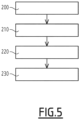
- the method further comprises a determination step 210, a pivoting step 220 and a second switching step 230.
- the determination step 210 is followed successively of the first switching step 200, the pivoting step 220 and the second switching step 230.
- a flowchart of steps 200 to 230 is shown on the figure 5 .
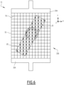
- This mode of implementation is particularly suitable for being implemented by large-sized devices 15.
- the operation of this mode of implementation is represented on the Figure 6 in the case of a device 15 comprising 16 conductors 30A, 30B, each comprising 14 (case of conductors 30A) or 28 (case of conductors 30B) second portions 55. It should be noted that the number of conductors 30A, 30B and second portions 55 may vary.
- first and second portions 50 and 55 are represented by thin lines, with the exception of the first portions 55 of the end conductors 30A, which are represented by thick lines.
- control module 20 determines a closed contour 85 on the support face 45.
- the closed contour 85 delimits a first zone on this face 45.
- the closed contour 85 has a maximum dimension and a minimum dimension measured in directions perpendicular to each other, the maximum dimension being strictly greater than the minimum dimension.
- the closed contour 85 is, thus, a non-circular contour.
- a ratio between the maximum dimension and the minimum dimension is, for example, greater than or equal to 3, in particular greater than or equal to 5, in particular greater than or equal to 10.
- the closed contour 85 is, for example, rectangular, as shown in the Figure 6 .
- the maximum dimension is the length of the longest side of the rectangle
- the minimum dimension is the length of the shortest side of the rectangle.
- the closed contour 85 is elliptical, in which case the maximum dimension is the major axis of the ellipse and the minimum dimension is the minor axis of the ellipse.
- the maximum dimension is the major axis of the ellipse and the minimum dimension is the minor axis of the ellipse.
- other forms are also possible.3
- the closed contour 85 has a surface area of between 10 ⁇ m 2 and 10 square centimeters (cm 2 ).
- the closed contour 85 surrounds a group of junctions 35 comprising at least 50 distinct junctions 35.
- the control module 20 controls the switching of each junction 35 included in the first zone towards its first configuration, and controls the switching of each junction 35 located outside the first zone in its second configuration.
- each junction 35 in its first configuration is represented by a cross, while the junctions 35 which are in their second configurations are not represented.
- control module 20 rotates the closed contour 85 around an axis parallel to the normal direction Z. This is represented symbolically on the Figure 6 by an arrow.
- control module 20 rotates the closed contour 85 by a predetermined angle during the pivoting step 220.
- the closed contour 85 delimits a second zone distinct from the first zone at the end of the pivoting step 220.
- control module 20 controls the switching of each junction 35 included in the second zone towards its first configuration, and controls the switching of each junction 35 located outside the second zone in its second configuration.
- Steps 200 to 230 are in particular repeated successively in the order detailed previously so as to rotate the closed contour 85 by 360 degrees (°) or more, depending on the number of iterations of steps 200 to 230.
- steps 200 to 230 are repeated so as to obtain periodic rotation of the closed contour with a rotation speed of between 100 degrees per second and 10,000 degrees per second.
- the rotation speed may vary.
- the switching of a junction 35 from the first to the second configuration does not significantly modify the electrical resistance of the junction, so that the electrical voltage between the end conductors 30A is not modified by the rotation of the contour 85.
- the electrical voltage between these two conductors 30A depends on the homogeneity of the magnetic field perceived by the different SQUIDs formed by the junctions 35 which are in their first configurations.
- the difference (in absolute value) between the value of the electric voltage in the presence of a magnetic field, for example the magnetic field of a radio frequency electromagnetic wave, and the value of the electric voltage in the absence of this magnetic field is all the more important as the magnetic field is homogeneous on the different SQUIDs.
- the closed contour 85 is such that the maximum dimension is measured in a direction perpendicular to the direction of propagation of the wave electromagnetic, the variation in voltage caused by the electromagnetic wave is maximum, while it is minimum when it is the minimum dimension which is measured in a direction perpendicular to the direction of propagation.
- the system 10 is an antenna, the system 10 is capable of determining the direction of propagation of an electromagnetic wave received by the device 15.
- the rotation speed of the closed contour 85 is likely to be much higher than the rotation speeds of the antennas of the state of the art in which the antenna, possibly comprising one or more SQUIDs, is mechanically rotated.
- junctions 35 having a first configuration and a second configuration are given below. Each of these examples of junction 35 can be used in a device 15 as defined above.
- control members 40 capable of switching the different examples of junctions 35 are also described.
- junction 35 A first example of junction 35 is shown on the Figure 7 .
- the barrier 63 is made of a second material, which is for example superconducting.
- the barrier 63 is made of the first material M1.
- the barrier 63 is electrically connected to the two second portions 55 which connect the junction 35 to the first portions 50 of the conductors 30A, 30B between which the junction 35 is interposed.
- the control member 40 comprises a ferroelectric layer 90 and a second electrode 95.
- the ferroelectric layer 90 is in contact with the barrier 63.
- the ferroelectric layer 90 and the barrier 63 are superimposed in a stacking direction which is in particular the normal direction Z, as shown in the Figure 7 .
- the stacking direction may vary.
- the ferroelectric layer 90 is made of a third material M3.
- An electrical polarization PE is defined for the third material M3. This means that the third material M3 has a plurality of electric dipoles each generating an electric moment, and the electric polarization PE is defined as being the average, per unit volume, of the electric moments.
- the electrical polarization PE is therefore a vector quantity.
- the third material M3 is a ferroelectric material.
- the PE polarization is mobile between a first orientation O1 and a second orientation O2.
- the PE polarization When the PE polarization is in the first orientation O1, the PE polarization has at least one component parallel to the stacking direction. This means that the first orientation O1 is not perpendicular to the stacking direction.
- the PE polarization When the PE polarization is in the second O2 orientation, the PE polarization has at least one component parallel to the stacking direction. The component is in the opposite direction to the direction of the first orientation O1.
- the first orientation O1 is parallel to the stacking direction.
- the PE polarization when the PE polarization is in the first orientation O1, the PE polarization is directed towards the barrier 63.
- the ferroelectric layer 90 is in particular interposed between the barrier 63 and the second electrode 95.
- the ferroelectric layer 90 is delimited in the stacking direction by the barrier 63 and by the second electrode 95.
- one or more layers additional are likely to be interposed between the ferroelectric layer 90 and one or the other of the barrier 63 and the second electrode 95.
- the control member 40 is, in particular, configured to control the direction of the PE polarization of the ferroelectric layer 90.
- control member 40 is capable of controlling the direction of the polarization PE via a voltage pulse between the second electrode 95 and one of the first electrodes 57.
- control member 40 is configured to impose, for a predetermined temporal duration, a potential difference V2 between the two faces of the ferroelectric layer 90 which delimit this layer 90 according to the stacking direction.
- control member 40 is configured to generate an electric current between a first electrode 57 and the second electrode 95.
- the voltage pulse modifies the orientation of the electrical polarization PE of the ferroelectric layer 90.
- the polarization PE when the sign of the potential difference V2 is positive, the polarization PE is rotated from the first orientation O1 to the second orientation O2. On the contrary, when the sign of the potential difference V2 is negative, the polarization PE is rotated from the second orientation O2 to the first orientation O1.
- the PE polarization causes the accumulation of electric charges in the barrier 63 when the PE polarization is in the first orientation O1.
- the accumulation of charge reduces the critical temperature of the barrier 63 from a first value T1 strictly greater than the set temperature Tc to a second value T2 strictly lower than the set temperature Tc.
- the second value T2 being strictly lower than the set temperature Tc, the barrier 63 is therefore not superconducting when the polarization PE is in the second orientation O2.
- control member 40 is capable of modifying the characteristics of the barrier 63 depending on whether the barrier 63 is superconducting or not at the set temperature Tc.
- the critical temperature and/or critical current values of the junction 35 are different depending on whether the barrier 63 is superconducting or not.
- the critical temperature and/or the critical current each have a strictly lower value when the barrier 63 is not superconducting than when the barrier 63 is superconducting.
- junction 35 forms a Josephson junction when barrier 63 is superconducting and prevents the passage of Cooper pairs between the two portions 55 when barrier 63 is not superconducting.
- junction 35 does not require the application of a voltage to remain in one or other of its configurations, and allows rapid switching.
- junction 35 and an associated control member 40 is shown on the figure 8 .
- the junction 35 comprises, in addition to the barrier 63, an electrically conductive layer 100.
- the barrier 63 is made of a non-superconductive material.
- the barrier 63 is made of an electrically insulating material.
- the barrier 63 is made of a material obtained by irradiation of first material M1 with an ion beam.
- such a material is obtained by irradiation of YBCO with oxygen or helium ions.
- the barrier 63 has a width, measured in the Y direction, of between 500 nm and 5 ⁇ m. In particular, the barrier 63 prevents the passage of Cooper pairs between the second portions 55. The barrier 63 is in particular in contact with the two second portions 55 to which the junction 35 is connected.
- the electrically conductive layer 100 is perpendicular to a stacking direction, which is for example the normal direction Z, although other directions are possible.
- the electrically conductive layer 100 is, for example, made of graphene. However, other electrically conductive materials are also possible, in particular materials having Dirac cones in their band structure.
- the electrically conductive layer 100 has a thickness less than or equal to 5 nm.
- the electrically conductive layer 100 is a monatomic layer.
- the electrically conductive layer 100 has a first face 105 and a second face 110.
- the first face 105 is in contact with the barrier 63.
- the first face 105 is in contact jointly with the barrier 63 and with the two portions 55, in particular with the ends of the two portions 55.
- the first face 105 is flat, in particular perpendicular to the stacking direction.
- the second face 110 is opposite the first face 105.
- the layer 100 is delimited by the first face 105 and the second face 110 in the stacking direction.
- the control member 40 comprises a configuration electrode 115 and a barrier layer 120.
- the configuration electrode 115 is made of an electrically conductive material, for example gold.
- the barrier layer 120 is interposed between the configuration electrode 115 and the electrically conductive layer 100. In particular, the barrier layer 120 is in contact with the second face 110.
- the barrier layer 120 is interposed between the configuration electrode 115 and the layer 100.
- the barrier layer 120 is made of an electrically insulating material, for example aluminum oxide.
- the control member 40 is configured to modify an electrical potential of the configuration electrode 120.
- the control member 40 is configured to modify an electric potential of the configuration electrode 120 between a third value and a fourth value.
- Switching the electric potential of the electrode 120 between the third and fourth values moves the Fermi level of the electrically conductive layer 100 between a fifth value and a sixth value.
- junction 35 is shown on the Figure 9 , with part of an associated control body 40.
- the junction 35 comprises, in addition to the barrier 63, at least two magnetic layers 125.
- the junction 35 is capable of allowing an electric current to flow from one of the corresponding second portions 55 to the other second portion 55, the electric current passing through the barrier 63 and the two magnetic layers 125.
- the magnetic layers 125 frame, for example, the barrier 63 in the second direction Y.
- each magnetic layer 125 is interposed between the barrier 63 and one of the corresponding second portions 55.
- the barrier 63 has a thickness of between 0.5 nm and 10 nm.
- the barrier 63 is capable of being crossed, by tunnel effect or by electrical conduction, by Cooper pairs. However, barrier 63 is not made of a superconducting material.
- barrier 63 is made of copper.
- Each layer 125 is made of a magnetic material.
- magnetic material will be used for a ferromagnetic material or a ferrimagnetic material.
- the magnetic moments are oriented parallel to each other.
- the magnetic moments of the material are oriented, remaining parallel to each other, in the direction of the external magnetic field.
- the magnetic moments are oriented antiparallel to each other, without perfectly compensating each other.
- the resultant of moments in a ferrimagnetic material is strictly less than the resultant of moments in this same material, if it were ferromagnetic.
- the magnetic moments of the material are oriented, while remaining antiparallel to each other, such that the resultant is oriented in the direction of the external magnetic field.
- Nickel Ni and permalloy NiFe are examples of magnetic materials.
- Each layer (125) is, for example, perpendicular to the Y direction.
- Each magnetic layer 125 has a thickness, measured along the second direction Y, of between 0.5 nm and 2.5 nm.
- the control member 40 is capable of modifying, in a known manner, the direction of magnetization of at least one of the magnetic layers 125.
- the direction of magnetization of one of the magnetic layers 125 is fixed while the direction of magnetization of the other magnetic layer 125 is mobile.
- Each direction of magnetization is, for example, perpendicular to the second direction Y.
- control member 40 comprises at least one configuration electrode 130, for example two configuration electrodes 130.
- the control member 40 is configured to generate an electric current passing through the configuration electrode, one of the magnetic layers 125, the barrier 63 and the other magnetic layer 125.
- the electric current passes through one of the configuration electrodes 130, part of a second portion 55, a magnetic layer 125, the barrier 63, the other magnetic layer 125, part of the other second portion 55 forming the junction 35 and the other configuration electrode 130.
- the variable direction of magnetization of one of the magnetic layers 125 pivots around an axis parallel to the second direction Y.
- the variable direction of magnetization is modified.
- an angle between the magnetization directions of the two magnetic layers 125 is modified.
- the control member 40 is capable of modifying an angle between the directions of magnetization by generating an electric current.
- the critical current of junction 35 is a function (in particular sinusoidal) of this phase shift.
- the critical current of the junction 35 depends on the angle between the directions of magnetization of the two magnetic layers 125.
- the critical current of the junction 35 has a value strictly lower than the value of the same magnitude when the magnetization directions are opposite.
- the junction 35 forms a Josephson junction whereas the junction 35 does not exhibit the Josephson effect when the directions of magnetization are opposite.
- barrier 35 and control member 40 A fourth example of barrier 35 and control member 40 will now be described.
- the barrier 63 comprises a portion made of a cuprate superconducting material.
- the control member 40 includes a configuration electrode in contact with the barrier 63.
- the configuration electrode is made of a metallic electronegative material, for example MoSi.
- the control member 40 is capable of controlling an electrical potential of the configuration electrode.
- the configuration electrode being electronegative, generates oxygen vacancies in the barrier 63.
- An oxygen vacancy is a location in the crystal lattice of the barrier 63 which should be occupied by an oxygen atom but which is unoccupied because the atoms of Oxygen are attracted to the electrode, part of which is oxidized by these atoms.
- the critical temperature of cuprates is a function of the amount of oxygen they contain. In particular, the higher the rate of oxygen vacancies, the more the critical temperature of the junction 35 decreases. Thus, the critical temperature Tc of the barrier 63 depends on the electric potential of the configuration electrode. The junction 35 then switches between its two configurations depending on whether the electric potential corresponds to a critical temperature Tc greater or lower than the temperature at which the junction 35 is located.
Landscapes
- Physics & Mathematics (AREA)
- Condensed Matter Physics & Semiconductors (AREA)
- General Physics & Mathematics (AREA)
- Superconductor Devices And Manufacturing Methods Thereof (AREA)
Claims (11)
- Vorrichtung (15) mit einem Substrat (25), einer Gruppe von elektrischen Leitern (30A, 30B), die von einer Seite (45) des Substrats (25) getragen werden, einer Gruppe von Übergängen (35), die von der genannten Seite (45) des Substrats (25) getragen werden, und einer Gruppe von Kontrollorganen (40),wobei jeder elektrische Leiter (30A, 30B) aus einem supraleitenden Material hergestellt ist, wobei jeder elektrische Leiter (30A, 30B) einen einzigen ersten Abschnitt (50), der sich in einer ersten Richtung (X) tangential zum Substrat (25) erstreckt, und eine Gruppe von zweiten Abschnitten (55) umfasst, wobei die ersten Abschnitte (50) der elektrischen Leiter (30A, 30B) nacheinander in Bezug aufeinander in einer zweiten Richtung (Y) senkrecht zur ersten Richtung (X) versetzt sind,wobei mindestens drei Übergänge (35) entlang der zweiten Richtung (Y) zwischen jedem Paar von aufeinanderfolgenden ersten Abschnitten (50) angeordnet sind, wobei jeder Übergang (35) mit dem ersten Abschnitt (50) jedes der Leiter (30A, 30B) verbunden ist, zwischen denen der Übergang (35), durch einen zweiten Abschnitt (55) des Leiters (30A, 30B) eingefügt ist,dadurch gekennzeichnet, dass jedes Steuerelement (40) einem einzelnen Übergang (35) aus der Gruppe von Übergängen (35) zugeordnet ist und so konfiguriert ist, dass es den zugeordneten Übergang (35) zwischen einer ersten Konfiguration, in der der Übergang (35) einen Josephson-Übergang zwischen den Leitern (30A, 30B) bildet, mit denen der Übergang (35) verbunden ist, und einer zweiten Konfiguration umschaltet, in der der Übergang (35) den Durchgang von Cooper-Paaren zwischen den Leitern (30A, 30B) verhindert.
- Vorrichtung nach Anspruch 1 mit mindestens zehn elektrischen Leitern (30A, 30B), wobei mindestens zehn Übergänge (35) zwischen jedem Paar aufeinanderfolgender erster Abschnitte (50) eingefügt sind.
- Vorrichtung nach Anspruch 1 oder 2, wobei sich jeder zweite Abschnitt (55) in der zweiten Richtung (Y) erstreckt.
- Vorrichtung nach einem der vorhergehenden Ansprüche, wobei jeder Übergang (35) eine Barriere (63) aufweist, die eine Sperre zwischen den beiden zweiten Abschnitten (55) bildet, die mit dem Übergang (35) verbunden sind, wobei mindestens eine der folgenden Eigenschaften überprüft wird:- die Barriere (63) ist aus einem ferroelektrischen Material mit einer elektrischen Polarisation hergestellt, wobei das Steuerelement (40) so konfiguriert ist, dass es eine Richtung der elektrischen Polarisation ändert;- die Barriere besteht (63) aus einem elektrisch isolierenden Material, der Übergang (35) weist außerdem eine elektrisch leitende Schicht (100) mit einer ersten Seite (105) auf, die mit den beiden zweiten Bereichen (55) in Kontakt steht, und eine zweite Seite (110), die der ersten Seite (105) gegenüberliegt, wobei das Steuerelement (40) eine elektrisch isolierende Sperrschicht (120) aufweist, die mit der zweiten Seite (110) in Kontakt ist, und eine Musterelektrode (115), wobei die Sperrschicht (120) zwischen der elektrisch leitenden Schicht (100) und der Musterelektrode (115) angeordnet ist, wobei das Steuerelement (40) so konfiguriert ist, dass es ein elektrisches Potential der Musterelektrode (115) ändert, wobei die elektrisch leitfähige Schicht (100) insbesondere aus Graphen gefertigt ist;- wobei der Übergang (35) mindestens zwei magnetische Schichten (125) aufweist, wobei jede magnetische Schicht (125) aus einem magnetischen Material besteht, der Übergang (35) so konfiguriert ist, dass er von einem elektrischen Strom durchflossen wird, der durch die Barriere (63) und die beiden magnetischen Schichten (125) fließt, wobei das Steuerelement (40) so konfiguriert ist, dass es eine Ausrichtung einer Magnetisierung von mindestens einer der magnetischen Schichten (125) ändert.
- Vorrichtung nach einem der vorhergehenden Ansprüche, die außerdem eine Ausgangselektrode (57), eine Eingangselektrode (57), eine elektrische Stromversorgung (42) und einen Sensor (43) umfasst, wobei die Stromversorgung (42) geeignet ist, einen elektrischen Strom in die Eingangselektrode (57) zu injizieren und eine Stromstärke des elektrischen Stroms auf einen vorbestimmten Wert zu bringen, wobei der elektrische Strom durch jeden der Leiter (30A, 30B) von der Eingangselektrode (57) zu der Ausgangselektrode (57) fließt, wobei der Sensor (43) dazu geeignet ist, eine elektrische Potentialdifferenz zwischen der Eingangselektrode (57) und der Ausgangselektrode (57) zu messen.
- Vorrichtung nach einem der vorhergehenden Ansprüche, bei der jeder erste oder zweite Abschnitt (50, 55) geradlinig ist.
- Vorrichtung nach einem der vorherigen Ansprüche, wobei:- ein Abstand, gemessen in der zweiten Richtung (Y) zwischen den beiden ersten Abschnitten (50) eines Paars aufeinanderfolgender Leiter (30A, 30B), für jedes Paar aufeinanderfolgender Leiter (30A, 30B) gleich ist, und/oder- ein Abstand, gemessen in der ersten Richtung (X) zwischen zwei aufeinanderfolgenden zweiten Abschnitten (55) eines gleichen elektrischen Leiters (30A, 30B), für jedes Paar von aufeinanderfolgenden zweiten Abschnitten (55) gleich ist.
- System (10) mit einem Steuermodul (20) und einer Vorrichtung (15) nach einem der vorhergehenden Ansprüche, wobei das System (10) insbesondere eine Antenne ist.
- System nach dem vorhergehenden Anspruch, wobei das Steuermodul (20) zu Folgendem konfiguriert ist:- Bestimmen (210) einer geschlossenen Kontur (85) auf der Fläche (45) des Substrats (25), die die Leiter (30A, 30B) und die Übergänge (35) trägt, wobei die geschlossene Kontur (85) einen ersten Bereich der Fläche (45) begrenzt,- Steuern eines Umschaltens (200) jedes Übergangs (35), der in dem ersten Bereich enthalten ist, auf die entsprechende erste Konfiguration und eines Umschaltens jedes Übergangs (35), der sich außerhalb des ersten Bereichs befindet, auf die entsprechende zweite Konfiguration,- Schwenken (220) der geschlossenen Kontur (85) um einen vorbestimmten Winkel um eine Achse senkrecht zu der Seite (45) des Substrats (25), die die Leiter (30A, 30B) und die Übergänge (35) trägt, wobei die geschlossene Kontur (85) nach dem Schwenken einen zweiten Bereich begrenzt, und- Steuern eines Umschaltens (230) jedes Übergangs (35), der in dem zweiten Bereich enthalten ist, auf die entsprechende erste Konfiguration und eines Umschaltens jedes Übergangs (35), der sich außerhalb des zweiten Bereichs befindet, auf die entsprechende zweite Konfiguration.
- Verfahren zur Verwendung einer Vorrichtung (15), die ein Substrat (25), eine Gruppe von elektrischen Leitern (30A, 30B), die von einem Substrat (25) getragen werden, eine Gruppe von Übergängen (35) und eine Gruppe von Steuerelementen (40) umfasst, wobei jeder elektrische Leiter (30A, 30B) aus einem supraleitenden Material hergestellt ist, wobei jeder elektrische Leiter (30A, 30B) einen einzigen ersten Abschnitt (50), der sich in einer ersten Richtung (X) tangential zum Substrat (25) erstreckt, und einen Satz von zweiten Abschnitten (55) umfasst, wobei die ersten Abschnitte (50) der elektrischen Leiter (30A, 30B) aufeinanderfolgend in Bezug zueinander in einer zweiten Richtung (Y) senkrecht zur ersten Richtung (X) versetzt sind, wobei mindestens drei Übergänge (35) in der zweiten Richtung (Y) zwischen jedem Paar aufeinanderfolgender erster Abschnitte (50) angeordnet sind, wobei jeder Übergang (35) mit dem ersten Abschnitt (50) jedes der Leiter (30A, 30B) zwischen denen der Übergang (35) durch einen zweiten Abschnitt (55) des Leiters eingefügt ist, dadurch gekennzeichnet dass das Verfahren einen Schritt des Umschaltens (200) mindestens einer Verbindung (35) zwischen einer ersten Konfiguration, in der die Verbindung (35) eine Josephson-Verbindung zwischen den Leitern (30A, 30B) bildet, mit denen die Verbindung (35) verbunden ist, und einer zweiten Konfiguration umfasst, in der die Verbindung (35) den Durchgang von Cooper-Paaren zwischen den Leitern (30A, 30B) verhindert.
- Verfahren nach dem vorhergehenden Anspruch, bei dem am Ende des Schaltschritts (200) jeder Übergang (35), der in einem ersten Bereich der Seite (45) des Substrats enthalten ist, die die Leiter (30A, 30B) und die Übergänge (35) trägt, in der ersten Konfiguration ist, wobei der erste Bereich durch eine geschlossene Kontur (85) auf der Fläche (45) begrenzt ist, wobei jeder Übergang (35), der außerhalb des ersten Bereichs angeordnet ist, in der zweiten Konfiguration ist, wobei das Verfahren ferner die folgenden Schritte umfasst:- Schwenken (220) der geschlossenen Kontur (85) um einen vorgegebenen Winkel um eine Achse senkrecht zur der Seite (45) des Substrats (25), die die Leiter (30A, 30B) und die Übergänge (35) trägt, wobei die geschlossene Kontur (85) auf der Seite (45) nach dem Schritt des Schwenkens (220) einen zweiten Bereich begrenzt, und- Umschalten (230) jedes Übergangs (35), der in dem zweiten Bereich enthalten ist, auf die entsprechende erste Konfiguration und Umschalten jedes Übergangs (35), der sich außerhalb des zweiten Bereichs befindet, auf die entsprechende zweite Konfiguration.
Applications Claiming Priority (2)
| Application Number | Priority Date | Filing Date | Title |
|---|---|---|---|
| FR2001129A FR3106934B1 (fr) | 2020-02-05 | 2020-02-05 | Dispositif comportant un ensemble de jonctions josephson, systeme comprenant un tel dispositif et procede d'utilisation d'un tel dispositif |
| PCT/EP2021/052682 WO2021156377A1 (fr) | 2020-02-05 | 2021-02-04 | Dispositif comportant un ensemble de jonctions josephson, système comprenant un tel dispositif et procédé d'utilisation d'un tel dispositif |
Publications (2)
| Publication Number | Publication Date |
|---|---|
| EP4101006A1 EP4101006A1 (de) | 2022-12-14 |
| EP4101006B1 true EP4101006B1 (de) | 2024-03-20 |
Family
ID=72178600
Family Applications (1)
| Application Number | Title | Priority Date | Filing Date |
|---|---|---|---|
| EP21702681.4A Active EP4101006B1 (de) | 2020-02-05 | 2021-02-04 | Vorrichtung mit einem satz von josephson-übergängen, system mit einer solchen vorrichtung und verfahren zur verwendung einer solchen vorrichtung |
Country Status (4)
| Country | Link |
|---|---|
| US (1) | US20230059096A1 (de) |
| EP (1) | EP4101006B1 (de) |
| FR (1) | FR3106934B1 (de) |
| WO (1) | WO2021156377A1 (de) |
Family Cites Families (9)
| Publication number | Priority date | Publication date | Assignee | Title |
|---|---|---|---|---|
| DE4137953C2 (de) * | 1991-11-18 | 1994-12-22 | Siemens Ag | Mikrowellenschaltkreis einer Josephson-Einrichtung und Verwendung des Schaltkreises |
| EP0823734A1 (de) * | 1996-07-23 | 1998-02-11 | DORNIER GmbH | Josephson-Übergangs-Array-Anordnung und Verfahren zu ihrer Herstellung |
| WO2008006217A1 (en) * | 2006-07-14 | 2008-01-17 | D-Wave Systems Inc. | Systems, methods, and apparatus for quasi-adiabatic quantum computation |
| WO2008137485A2 (en) * | 2007-05-04 | 2008-11-13 | California Institute Of Technology | Low field squid mri devices, components and methods |
| US8812066B2 (en) * | 2008-10-09 | 2014-08-19 | D-Wave Systems Inc. | Systems, methods and apparatus for measuring magnetic fields |
| EP3138052B1 (de) * | 2014-05-01 | 2021-07-07 | Lockheed Martin Corporation | Quantenassistiertes training von neuronalen netzen |
| US10224475B2 (en) * | 2014-06-11 | 2019-03-05 | The Regents Of The University Of California | Method for fabricating superconducting devices using a focused ion beam |
| US12161052B2 (en) * | 2018-03-06 | 2024-12-03 | Cornell University | Expitaxial semiconductor/superconductor heterostructures |
| GB2606356A (en) * | 2021-05-04 | 2022-11-09 | Iqe Plc | A layered structure |
-
2020
- 2020-02-05 FR FR2001129A patent/FR3106934B1/fr active Active
-
2021
- 2021-02-04 WO PCT/EP2021/052682 patent/WO2021156377A1/fr not_active Ceased
- 2021-02-04 US US17/797,292 patent/US20230059096A1/en active Pending
- 2021-02-04 EP EP21702681.4A patent/EP4101006B1/de active Active
Also Published As
| Publication number | Publication date |
|---|---|
| WO2021156377A1 (fr) | 2021-08-12 |
| US20230059096A1 (en) | 2023-02-23 |
| FR3106934A1 (fr) | 2021-08-06 |
| FR3106934B1 (fr) | 2022-07-22 |
| EP4101006A1 (de) | 2022-12-14 |
Similar Documents
| Publication | Publication Date | Title |
|---|---|---|
| EP1506581B1 (de) | Supraleitende quanten-bit-einrichtung mit josephson-übergängen | |
| CH628993A5 (fr) | Appareil de detection d'un champ magnetique exterieur. | |
| WO2013007797A1 (fr) | Oscillateur spintronique et utilisation de celui-ci dans des dispositifs radiofréquence | |
| FR3084505A1 (fr) | Reseau de neurones comportant des resonateurs spintroniques | |
| EP4101006B1 (de) | Vorrichtung mit einem satz von josephson-übergängen, system mit einer solchen vorrichtung und verfahren zur verwendung einer solchen vorrichtung | |
| WO2020021101A1 (fr) | Chaîne synaptique comprenant des résonateurs spintroniques basés sur l'effet de diode de spin et réseau de neurones comprenant une telle chaîne synaptique | |
| EP2543135B1 (de) | Magnetoresistiver hf-oszillator und verfahren zur erzeugung eines schwingungssignals | |
| EP2945160B1 (de) | Elektronische komponente mit josephson-kontakt | |
| FR2775832A1 (fr) | Systeme semiconducteur de test realise dans un chemin de decoupe d'une plaquette semiconductrice | |
| EP3053202B1 (de) | Verfahren zur herstellung eines josephson-übergangs und zugehöriger josephson-übergang | |
| EP3143694B1 (de) | Spintronic logikschaltung mit spin polarisiertem stromschalter und integrierter schaltung | |
| WO2020239957A1 (fr) | Procédé de conception d'un composant supraconducteur et dispositifs associés | |
| FR2626109A1 (fr) | Dispositifs de visualisation de rayonnement thermique, systemes comportant de tels dispositifs, et methode de fabrication de tels dispositifs de visualisation | |
| EP0923142B1 (de) | Supraleitende Tunneleffektdetektorzelle | |
| FR3114645A1 (fr) | Détecteur à inductance cinétique | |
| EP3827378A1 (de) | Synaptische kette mit spintronik-resonatoren auf basis des inversen spin-hall-effekts und neuronales netz mit solch einer synaptischen kette | |
| Anderson et al. | Feasibility of enhanced microwave image resolution using a superdirective aperture | |
| JP2730502B2 (ja) | 超電導トランジスタ | |
| FR2463512A1 (fr) | Perfectionnements aux dispositifs a jonctions tunnel et aux procedes de fabrication de telles jonctions | |
| Yoshida et al. | Interface-engineered junctions with YbBaCuO as the counter-electrode | |
| JP2759508B2 (ja) | 光検出器 | |
| WO2022053502A1 (fr) | Dispositif implémentant un filtre convolutionnel d'un réseau de neurones | |
| Yu | Photoinduced carriers in insulating cuprates: Fermi-glass state, metal-insulator transition and superconductivity | |
| WO2017198866A1 (fr) | Dispositif comprenant une jonction josephson | |
| Lathrop | Josephson properties of high-temperature superconducting yttrium barium copper oxide grain boundary weak links |
Legal Events
| Date | Code | Title | Description |
|---|---|---|---|
| STAA | Information on the status of an ep patent application or granted ep patent |
Free format text: STATUS: UNKNOWN |
|
| STAA | Information on the status of an ep patent application or granted ep patent |
Free format text: STATUS: THE INTERNATIONAL PUBLICATION HAS BEEN MADE |
|
| PUAI | Public reference made under article 153(3) epc to a published international application that has entered the european phase |
Free format text: ORIGINAL CODE: 0009012 |
|
| STAA | Information on the status of an ep patent application or granted ep patent |
Free format text: STATUS: REQUEST FOR EXAMINATION WAS MADE |
|
| 17P | Request for examination filed |
Effective date: 20220804 |
|
| AK | Designated contracting states |
Kind code of ref document: A1 Designated state(s): AL AT BE BG CH CY CZ DE DK EE ES FI FR GB GR HR HU IE IS IT LI LT LU LV MC MK MT NL NO PL PT RO RS SE SI SK SM TR |
|
| DAV | Request for validation of the european patent (deleted) | ||
| DAX | Request for extension of the european patent (deleted) | ||
| REG | Reference to a national code |
Ref country code: DE Ref legal event code: R079 Ref country code: DE Ref legal event code: R079 Ref document number: 602021010655 Country of ref document: DE Free format text: PREVIOUS MAIN CLASS: H01L0027180000 Ipc: H10N0060120000 |
|
| RIC1 | Information provided on ipc code assigned before grant |
Ipc: G06N 10/00 20220101ALN20230907BHEP Ipc: G06N 3/065 20230101ALN20230907BHEP Ipc: H10N 69/00 20230101ALI20230907BHEP Ipc: H10N 60/10 20230101ALI20230907BHEP Ipc: H10N 60/12 20230101AFI20230907BHEP |
|
| GRAP | Despatch of communication of intention to grant a patent |
Free format text: ORIGINAL CODE: EPIDOSNIGR1 |
|
| STAA | Information on the status of an ep patent application or granted ep patent |
Free format text: STATUS: GRANT OF PATENT IS INTENDED |
|
| INTG | Intention to grant announced |
Effective date: 20231013 |
|
| RIN1 | Information on inventor provided before grant (corrected) |
Inventor name: DLUBAK, BRUNO Inventor name: ROUCO GOMEZ, VICTOR Inventor name: PERCONTE, DAVID Inventor name: LEMAITRE, YVES, ERIC, JACQUES Inventor name: SENEOR, PIERRE Inventor name: MARCILHAC, BRUNO Inventor name: VILLEGAS, JAVIER E. Inventor name: TRASTOY QUINTELA, JUAN |
|
| GRAS | Grant fee paid |
Free format text: ORIGINAL CODE: EPIDOSNIGR3 |
|
| GRAA | (expected) grant |
Free format text: ORIGINAL CODE: 0009210 |
|
| STAA | Information on the status of an ep patent application or granted ep patent |
Free format text: STATUS: THE PATENT HAS BEEN GRANTED |
|
| AK | Designated contracting states |
Kind code of ref document: B1 Designated state(s): AL AT BE BG CH CY CZ DE DK EE ES FI FR GB GR HR HU IE IS IT LI LT LU LV MC MK MT NL NO PL PT RO RS SE SI SK SM TR |
|
| REG | Reference to a national code |
Ref country code: GB Ref legal event code: FG4D Free format text: NOT ENGLISH |
|
| REG | Reference to a national code |
Ref country code: CH Ref legal event code: EP |
|
| REG | Reference to a national code |
Ref country code: IE Ref legal event code: FG4D Free format text: LANGUAGE OF EP DOCUMENT: FRENCH |
|
| REG | Reference to a national code |
Ref country code: DE Ref legal event code: R096 Ref document number: 602021010655 Country of ref document: DE |
|
| PG25 | Lapsed in a contracting state [announced via postgrant information from national office to epo] |
Ref country code: LT Free format text: LAPSE BECAUSE OF FAILURE TO SUBMIT A TRANSLATION OF THE DESCRIPTION OR TO PAY THE FEE WITHIN THE PRESCRIBED TIME-LIMIT Effective date: 20240320 |
|
| REG | Reference to a national code |
Ref country code: LT Ref legal event code: MG9D |
|
| PG25 | Lapsed in a contracting state [announced via postgrant information from national office to epo] |
Ref country code: GR Free format text: LAPSE BECAUSE OF FAILURE TO SUBMIT A TRANSLATION OF THE DESCRIPTION OR TO PAY THE FEE WITHIN THE PRESCRIBED TIME-LIMIT Effective date: 20240621 |
|
| PG25 | Lapsed in a contracting state [announced via postgrant information from national office to epo] |
Ref country code: RS Free format text: LAPSE BECAUSE OF FAILURE TO SUBMIT A TRANSLATION OF THE DESCRIPTION OR TO PAY THE FEE WITHIN THE PRESCRIBED TIME-LIMIT Effective date: 20240620 Ref country code: HR Free format text: LAPSE BECAUSE OF FAILURE TO SUBMIT A TRANSLATION OF THE DESCRIPTION OR TO PAY THE FEE WITHIN THE PRESCRIBED TIME-LIMIT Effective date: 20240320 |
|
| REG | Reference to a national code |
Ref country code: NL Ref legal event code: MP Effective date: 20240320 |
|
| PG25 | Lapsed in a contracting state [announced via postgrant information from national office to epo] |
Ref country code: RS Free format text: LAPSE BECAUSE OF FAILURE TO SUBMIT A TRANSLATION OF THE DESCRIPTION OR TO PAY THE FEE WITHIN THE PRESCRIBED TIME-LIMIT Effective date: 20240620 Ref country code: NO Free format text: LAPSE BECAUSE OF FAILURE TO SUBMIT A TRANSLATION OF THE DESCRIPTION OR TO PAY THE FEE WITHIN THE PRESCRIBED TIME-LIMIT Effective date: 20240620 Ref country code: LT Free format text: LAPSE BECAUSE OF FAILURE TO SUBMIT A TRANSLATION OF THE DESCRIPTION OR TO PAY THE FEE WITHIN THE PRESCRIBED TIME-LIMIT Effective date: 20240320 Ref country code: HR Free format text: LAPSE BECAUSE OF FAILURE TO SUBMIT A TRANSLATION OF THE DESCRIPTION OR TO PAY THE FEE WITHIN THE PRESCRIBED TIME-LIMIT Effective date: 20240320 Ref country code: GR Free format text: LAPSE BECAUSE OF FAILURE TO SUBMIT A TRANSLATION OF THE DESCRIPTION OR TO PAY THE FEE WITHIN THE PRESCRIBED TIME-LIMIT Effective date: 20240621 Ref country code: FI Free format text: LAPSE BECAUSE OF FAILURE TO SUBMIT A TRANSLATION OF THE DESCRIPTION OR TO PAY THE FEE WITHIN THE PRESCRIBED TIME-LIMIT Effective date: 20240320 Ref country code: BG Free format text: LAPSE BECAUSE OF FAILURE TO SUBMIT A TRANSLATION OF THE DESCRIPTION OR TO PAY THE FEE WITHIN THE PRESCRIBED TIME-LIMIT Effective date: 20240320 |
|
| REG | Reference to a national code |
Ref country code: AT Ref legal event code: MK05 Ref document number: 1668973 Country of ref document: AT Kind code of ref document: T Effective date: 20240320 |
|
| PG25 | Lapsed in a contracting state [announced via postgrant information from national office to epo] |
Ref country code: SE Free format text: LAPSE BECAUSE OF FAILURE TO SUBMIT A TRANSLATION OF THE DESCRIPTION OR TO PAY THE FEE WITHIN THE PRESCRIBED TIME-LIMIT Effective date: 20240320 Ref country code: LV Free format text: LAPSE BECAUSE OF FAILURE TO SUBMIT A TRANSLATION OF THE DESCRIPTION OR TO PAY THE FEE WITHIN THE PRESCRIBED TIME-LIMIT Effective date: 20240320 |
|
| PG25 | Lapsed in a contracting state [announced via postgrant information from national office to epo] |
Ref country code: NL Free format text: LAPSE BECAUSE OF FAILURE TO SUBMIT A TRANSLATION OF THE DESCRIPTION OR TO PAY THE FEE WITHIN THE PRESCRIBED TIME-LIMIT Effective date: 20240320 |
|
| PG25 | Lapsed in a contracting state [announced via postgrant information from national office to epo] |
Ref country code: NL Free format text: LAPSE BECAUSE OF FAILURE TO SUBMIT A TRANSLATION OF THE DESCRIPTION OR TO PAY THE FEE WITHIN THE PRESCRIBED TIME-LIMIT Effective date: 20240320 |
|
| PG25 | Lapsed in a contracting state [announced via postgrant information from national office to epo] |
Ref country code: IS Free format text: LAPSE BECAUSE OF FAILURE TO SUBMIT A TRANSLATION OF THE DESCRIPTION OR TO PAY THE FEE WITHIN THE PRESCRIBED TIME-LIMIT Effective date: 20240720 |
|
| PG25 | Lapsed in a contracting state [announced via postgrant information from national office to epo] |
Ref country code: SM Free format text: LAPSE BECAUSE OF FAILURE TO SUBMIT A TRANSLATION OF THE DESCRIPTION OR TO PAY THE FEE WITHIN THE PRESCRIBED TIME-LIMIT Effective date: 20240320 Ref country code: PT Free format text: LAPSE BECAUSE OF FAILURE TO SUBMIT A TRANSLATION OF THE DESCRIPTION OR TO PAY THE FEE WITHIN THE PRESCRIBED TIME-LIMIT Effective date: 20240722 |
|
| PG25 | Lapsed in a contracting state [announced via postgrant information from national office to epo] |
Ref country code: ES Free format text: LAPSE BECAUSE OF FAILURE TO SUBMIT A TRANSLATION OF THE DESCRIPTION OR TO PAY THE FEE WITHIN THE PRESCRIBED TIME-LIMIT Effective date: 20240320 |
|
| PG25 | Lapsed in a contracting state [announced via postgrant information from national office to epo] |
Ref country code: EE Free format text: LAPSE BECAUSE OF FAILURE TO SUBMIT A TRANSLATION OF THE DESCRIPTION OR TO PAY THE FEE WITHIN THE PRESCRIBED TIME-LIMIT Effective date: 20240320 Ref country code: CZ Free format text: LAPSE BECAUSE OF FAILURE TO SUBMIT A TRANSLATION OF THE DESCRIPTION OR TO PAY THE FEE WITHIN THE PRESCRIBED TIME-LIMIT Effective date: 20240320 |
|
| PG25 | Lapsed in a contracting state [announced via postgrant information from national office to epo] |
Ref country code: AT Free format text: LAPSE BECAUSE OF FAILURE TO SUBMIT A TRANSLATION OF THE DESCRIPTION OR TO PAY THE FEE WITHIN THE PRESCRIBED TIME-LIMIT Effective date: 20240320 |
|
| PG25 | Lapsed in a contracting state [announced via postgrant information from national office to epo] |
Ref country code: PL Free format text: LAPSE BECAUSE OF FAILURE TO SUBMIT A TRANSLATION OF THE DESCRIPTION OR TO PAY THE FEE WITHIN THE PRESCRIBED TIME-LIMIT Effective date: 20240320 |
|
| PG25 | Lapsed in a contracting state [announced via postgrant information from national office to epo] |
Ref country code: SK Free format text: LAPSE BECAUSE OF FAILURE TO SUBMIT A TRANSLATION OF THE DESCRIPTION OR TO PAY THE FEE WITHIN THE PRESCRIBED TIME-LIMIT Effective date: 20240320 |
|
| PG25 | Lapsed in a contracting state [announced via postgrant information from national office to epo] |
Ref country code: SM Free format text: LAPSE BECAUSE OF FAILURE TO SUBMIT A TRANSLATION OF THE DESCRIPTION OR TO PAY THE FEE WITHIN THE PRESCRIBED TIME-LIMIT Effective date: 20240320 Ref country code: SK Free format text: LAPSE BECAUSE OF FAILURE TO SUBMIT A TRANSLATION OF THE DESCRIPTION OR TO PAY THE FEE WITHIN THE PRESCRIBED TIME-LIMIT Effective date: 20240320 Ref country code: RO Free format text: LAPSE BECAUSE OF FAILURE TO SUBMIT A TRANSLATION OF THE DESCRIPTION OR TO PAY THE FEE WITHIN THE PRESCRIBED TIME-LIMIT Effective date: 20240320 Ref country code: PT Free format text: LAPSE BECAUSE OF FAILURE TO SUBMIT A TRANSLATION OF THE DESCRIPTION OR TO PAY THE FEE WITHIN THE PRESCRIBED TIME-LIMIT Effective date: 20240722 Ref country code: PL Free format text: LAPSE BECAUSE OF FAILURE TO SUBMIT A TRANSLATION OF THE DESCRIPTION OR TO PAY THE FEE WITHIN THE PRESCRIBED TIME-LIMIT Effective date: 20240320 Ref country code: IS Free format text: LAPSE BECAUSE OF FAILURE TO SUBMIT A TRANSLATION OF THE DESCRIPTION OR TO PAY THE FEE WITHIN THE PRESCRIBED TIME-LIMIT Effective date: 20240720 Ref country code: ES Free format text: LAPSE BECAUSE OF FAILURE TO SUBMIT A TRANSLATION OF THE DESCRIPTION OR TO PAY THE FEE WITHIN THE PRESCRIBED TIME-LIMIT Effective date: 20240320 Ref country code: EE Free format text: LAPSE BECAUSE OF FAILURE TO SUBMIT A TRANSLATION OF THE DESCRIPTION OR TO PAY THE FEE WITHIN THE PRESCRIBED TIME-LIMIT Effective date: 20240320 Ref country code: CZ Free format text: LAPSE BECAUSE OF FAILURE TO SUBMIT A TRANSLATION OF THE DESCRIPTION OR TO PAY THE FEE WITHIN THE PRESCRIBED TIME-LIMIT Effective date: 20240320 Ref country code: AT Free format text: LAPSE BECAUSE OF FAILURE TO SUBMIT A TRANSLATION OF THE DESCRIPTION OR TO PAY THE FEE WITHIN THE PRESCRIBED TIME-LIMIT Effective date: 20240320 |
|
| PG25 | Lapsed in a contracting state [announced via postgrant information from national office to epo] |
Ref country code: IT Free format text: LAPSE BECAUSE OF FAILURE TO SUBMIT A TRANSLATION OF THE DESCRIPTION OR TO PAY THE FEE WITHIN THE PRESCRIBED TIME-LIMIT Effective date: 20240320 |
|
| REG | Reference to a national code |
Ref country code: DE Ref legal event code: R097 Ref document number: 602021010655 Country of ref document: DE |
|
| PG25 | Lapsed in a contracting state [announced via postgrant information from national office to epo] |
Ref country code: IT Free format text: LAPSE BECAUSE OF FAILURE TO SUBMIT A TRANSLATION OF THE DESCRIPTION OR TO PAY THE FEE WITHIN THE PRESCRIBED TIME-LIMIT Effective date: 20240320 |
|
| PG25 | Lapsed in a contracting state [announced via postgrant information from national office to epo] |
Ref country code: DK Free format text: LAPSE BECAUSE OF FAILURE TO SUBMIT A TRANSLATION OF THE DESCRIPTION OR TO PAY THE FEE WITHIN THE PRESCRIBED TIME-LIMIT Effective date: 20240320 |
|
| PLBE | No opposition filed within time limit |
Free format text: ORIGINAL CODE: 0009261 |
|
| STAA | Information on the status of an ep patent application or granted ep patent |
Free format text: STATUS: NO OPPOSITION FILED WITHIN TIME LIMIT |
|
| PG25 | Lapsed in a contracting state [announced via postgrant information from national office to epo] |
Ref country code: DK Free format text: LAPSE BECAUSE OF FAILURE TO SUBMIT A TRANSLATION OF THE DESCRIPTION OR TO PAY THE FEE WITHIN THE PRESCRIBED TIME-LIMIT Effective date: 20240320 |
|
| 26N | No opposition filed |
Effective date: 20241223 |
|
| PG25 | Lapsed in a contracting state [announced via postgrant information from national office to epo] |
Ref country code: SI Free format text: LAPSE BECAUSE OF FAILURE TO SUBMIT A TRANSLATION OF THE DESCRIPTION OR TO PAY THE FEE WITHIN THE PRESCRIBED TIME-LIMIT Effective date: 20240320 |
|
| PG25 | Lapsed in a contracting state [announced via postgrant information from national office to epo] |
Ref country code: MC Free format text: LAPSE BECAUSE OF FAILURE TO SUBMIT A TRANSLATION OF THE DESCRIPTION OR TO PAY THE FEE WITHIN THE PRESCRIBED TIME-LIMIT Effective date: 20240320 |
|
| REG | Reference to a national code |
Ref country code: CH Ref legal event code: PL |
|
| PG25 | Lapsed in a contracting state [announced via postgrant information from national office to epo] |
Ref country code: LU Free format text: LAPSE BECAUSE OF NON-PAYMENT OF DUE FEES Effective date: 20250204 |
|
| PG25 | Lapsed in a contracting state [announced via postgrant information from national office to epo] |
Ref country code: CH Free format text: LAPSE BECAUSE OF NON-PAYMENT OF DUE FEES Effective date: 20250228 |
|
| GBPC | Gb: european patent ceased through non-payment of renewal fee |
Effective date: 20250204 |
|
| REG | Reference to a national code |
Ref country code: BE Ref legal event code: MM Effective date: 20250228 |
|
| PG25 | Lapsed in a contracting state [announced via postgrant information from national office to epo] |
Ref country code: GB Free format text: LAPSE BECAUSE OF NON-PAYMENT OF DUE FEES Effective date: 20250204 |
|
| PG25 | Lapsed in a contracting state [announced via postgrant information from national office to epo] |
Ref country code: BE Free format text: LAPSE BECAUSE OF NON-PAYMENT OF DUE FEES Effective date: 20250228 |
|
| PG25 | Lapsed in a contracting state [announced via postgrant information from national office to epo] |
Ref country code: IE Free format text: LAPSE BECAUSE OF NON-PAYMENT OF DUE FEES Effective date: 20250204 |
|
| PGFP | Annual fee paid to national office [announced via postgrant information from national office to epo] |
Ref country code: DE Payment date: 20260206 Year of fee payment: 6 |
|
| PGFP | Annual fee paid to national office [announced via postgrant information from national office to epo] |
Ref country code: FR Payment date: 20260227 Year of fee payment: 6 |