EP4102578A1 - Elektrisches verbindungselement für mindestens zwei fotovoltaikzellen - Google Patents
Elektrisches verbindungselement für mindestens zwei fotovoltaikzellen Download PDFInfo
- Publication number
- EP4102578A1 EP4102578A1 EP22177283.3A EP22177283A EP4102578A1 EP 4102578 A1 EP4102578 A1 EP 4102578A1 EP 22177283 A EP22177283 A EP 22177283A EP 4102578 A1 EP4102578 A1 EP 4102578A1
- Authority
- EP
- European Patent Office
- Prior art keywords
- interconnection element
- photovoltaic
- photovoltaic cells
- assembly according
- interconnection
- Prior art date
- Legal status (The legal status is an assumption and is not a legal conclusion. Google has not performed a legal analysis and makes no representation as to the accuracy of the status listed.)
- Pending
Links
- 239000004020 conductor Substances 0.000 claims abstract description 16
- 238000013519 translation Methods 0.000 claims abstract description 7
- 230000004907 flux Effects 0.000 claims description 6
- 238000000034 method Methods 0.000 claims description 5
- 230000008859 change Effects 0.000 claims description 3
- 241000257303 Hymenoptera Species 0.000 claims 1
- 210000004027 cell Anatomy 0.000 description 105
- 239000010410 layer Substances 0.000 description 15
- 239000000463 material Substances 0.000 description 12
- 229920000642 polymer Polymers 0.000 description 8
- 238000004519 manufacturing process Methods 0.000 description 7
- 239000011248 coating agent Substances 0.000 description 6
- 238000000576 coating method Methods 0.000 description 6
- 229910052751 metal Inorganic materials 0.000 description 6
- 239000002184 metal Substances 0.000 description 6
- 229910001092 metal group alloy Inorganic materials 0.000 description 6
- RYGMFSIKBFXOCR-UHFFFAOYSA-N Copper Chemical compound [Cu] RYGMFSIKBFXOCR-UHFFFAOYSA-N 0.000 description 5
- BQCADISMDOOEFD-UHFFFAOYSA-N Silver Chemical compound [Ag] BQCADISMDOOEFD-UHFFFAOYSA-N 0.000 description 5
- 229910045601 alloy Inorganic materials 0.000 description 5
- 239000000956 alloy Substances 0.000 description 5
- 238000013459 approach Methods 0.000 description 5
- 239000010949 copper Substances 0.000 description 5
- 238000003475 lamination Methods 0.000 description 5
- 238000002844 melting Methods 0.000 description 5
- 230000008018 melting Effects 0.000 description 5
- 229910052709 silver Inorganic materials 0.000 description 5
- 239000004332 silver Substances 0.000 description 5
- 238000003466 welding Methods 0.000 description 5
- XEEYBQQBJWHFJM-UHFFFAOYSA-N Iron Chemical compound [Fe] XEEYBQQBJWHFJM-UHFFFAOYSA-N 0.000 description 4
- 239000012790 adhesive layer Substances 0.000 description 4
- 238000000429 assembly Methods 0.000 description 4
- 229910052802 copper Inorganic materials 0.000 description 4
- 239000011521 glass Substances 0.000 description 4
- 238000001465 metallisation Methods 0.000 description 4
- 150000002739 metals Chemical class 0.000 description 4
- PXHVJJICTQNCMI-UHFFFAOYSA-N nickel Substances [Ni] PXHVJJICTQNCMI-UHFFFAOYSA-N 0.000 description 4
- 230000005855 radiation Effects 0.000 description 4
- 239000000853 adhesive Substances 0.000 description 3
- 230000001070 adhesive effect Effects 0.000 description 3
- 230000008901 benefit Effects 0.000 description 3
- 230000005611 electricity Effects 0.000 description 3
- 229910052759 nickel Inorganic materials 0.000 description 3
- 230000000930 thermomechanical effect Effects 0.000 description 3
- 229910000640 Fe alloy Inorganic materials 0.000 description 2
- 229910001374 Invar Inorganic materials 0.000 description 2
- 239000004696 Poly ether ether ketone Substances 0.000 description 2
- QKAJPFXKNNXMIZ-UHFFFAOYSA-N [Bi].[Ag].[Sn] Chemical compound [Bi].[Ag].[Sn] QKAJPFXKNNXMIZ-UHFFFAOYSA-N 0.000 description 2
- 230000000712 assembly Effects 0.000 description 2
- 230000015572 biosynthetic process Effects 0.000 description 2
- 239000006059 cover glass Substances 0.000 description 2
- 238000013461 design Methods 0.000 description 2
- 238000005538 encapsulation Methods 0.000 description 2
- 230000007613 environmental effect Effects 0.000 description 2
- 229910052742 iron Inorganic materials 0.000 description 2
- 229910000833 kovar Inorganic materials 0.000 description 2
- 239000004033 plastic Substances 0.000 description 2
- 238000007747 plating Methods 0.000 description 2
- 229920002530 polyetherether ketone Polymers 0.000 description 2
- 239000000758 substrate Substances 0.000 description 2
- 238000010146 3D printing Methods 0.000 description 1
- 229910000531 Co alloy Inorganic materials 0.000 description 1
- CWYNVVGOOAEACU-UHFFFAOYSA-N Fe2+ Chemical compound [Fe+2] CWYNVVGOOAEACU-UHFFFAOYSA-N 0.000 description 1
- 229910001030 Iron–nickel alloy Inorganic materials 0.000 description 1
- ZOKXTWBITQBERF-UHFFFAOYSA-N Molybdenum Chemical compound [Mo] ZOKXTWBITQBERF-UHFFFAOYSA-N 0.000 description 1
- 229910000990 Ni alloy Inorganic materials 0.000 description 1
- 239000004642 Polyimide Substances 0.000 description 1
- ATJFFYVFTNAWJD-UHFFFAOYSA-N Tin Chemical compound [Sn] ATJFFYVFTNAWJD-UHFFFAOYSA-N 0.000 description 1
- 229920000508 Vectran Polymers 0.000 description 1
- 239000004979 Vectran Substances 0.000 description 1
- QXZUUHYBWMWJHK-UHFFFAOYSA-N [Co].[Ni] Chemical compound [Co].[Ni] QXZUUHYBWMWJHK-UHFFFAOYSA-N 0.000 description 1
- 229910052782 aluminium Inorganic materials 0.000 description 1
- XAGFODPZIPBFFR-UHFFFAOYSA-N aluminium Chemical compound [Al] XAGFODPZIPBFFR-UHFFFAOYSA-N 0.000 description 1
- 239000004760 aramid Substances 0.000 description 1
- 229920003235 aromatic polyamide Polymers 0.000 description 1
- 238000004364 calculation method Methods 0.000 description 1
- 238000006243 chemical reaction Methods 0.000 description 1
- 229910017052 cobalt Inorganic materials 0.000 description 1
- 239000010941 cobalt Substances 0.000 description 1
- GUTLYIVDDKVIGB-UHFFFAOYSA-N cobalt atom Chemical compound [Co] GUTLYIVDDKVIGB-UHFFFAOYSA-N 0.000 description 1
- 238000001816 cooling Methods 0.000 description 1
- -1 copper or silver Chemical class 0.000 description 1
- 238000004132 cross linking Methods 0.000 description 1
- 229910021419 crystalline silicon Inorganic materials 0.000 description 1
- 238000011161 development Methods 0.000 description 1
- 230000010339 dilation Effects 0.000 description 1
- 239000008393 encapsulating agent Substances 0.000 description 1
- 238000005516 engineering process Methods 0.000 description 1
- 230000004927 fusion Effects 0.000 description 1
- 238000002955 isolation Methods 0.000 description 1
- 229910052748 manganese Inorganic materials 0.000 description 1
- 239000011159 matrix material Substances 0.000 description 1
- 239000002923 metal particle Substances 0.000 description 1
- 238000012986 modification Methods 0.000 description 1
- 230000004048 modification Effects 0.000 description 1
- 229910052750 molybdenum Inorganic materials 0.000 description 1
- 239000011733 molybdenum Substances 0.000 description 1
- 229910021421 monocrystalline silicon Inorganic materials 0.000 description 1
- 230000005693 optoelectronics Effects 0.000 description 1
- 229920003223 poly(pyromellitimide-1,4-diphenyl ether) Polymers 0.000 description 1
- 229910021420 polycrystalline silicon Inorganic materials 0.000 description 1
- 229920001721 polyimide Polymers 0.000 description 1
- 229920006254 polymer film Polymers 0.000 description 1
- 239000002861 polymer material Substances 0.000 description 1
- 230000008569 process Effects 0.000 description 1
- 230000001681 protective effect Effects 0.000 description 1
- 238000011084 recovery Methods 0.000 description 1
- 230000009467 reduction Effects 0.000 description 1
- 238000012552 review Methods 0.000 description 1
- 238000005096 rolling process Methods 0.000 description 1
- 230000035939 shock Effects 0.000 description 1
- 229910052710 silicon Inorganic materials 0.000 description 1
- 239000007787 solid Substances 0.000 description 1
- 238000001228 spectrum Methods 0.000 description 1
- 238000005382 thermal cycling Methods 0.000 description 1
- 239000012815 thermoplastic material Substances 0.000 description 1
- 238000009941 weaving Methods 0.000 description 1
Images


Classifications
-
- H—ELECTRICITY
- H10—SEMICONDUCTOR DEVICES; ELECTRIC SOLID-STATE DEVICES NOT OTHERWISE PROVIDED FOR
- H10F—INORGANIC SEMICONDUCTOR DEVICES SENSITIVE TO INFRARED RADIATION, LIGHT, ELECTROMAGNETIC RADIATION OF SHORTER WAVELENGTH OR CORPUSCULAR RADIATION
- H10F19/00—Integrated devices, or assemblies of multiple devices, comprising at least one photovoltaic cell covered by group H10F10/00, e.g. photovoltaic modules
- H10F19/90—Structures for connecting between photovoltaic cells, e.g. interconnections or insulating spacers
- H10F19/902—Structures for connecting between photovoltaic cells, e.g. interconnections or insulating spacers for series or parallel connection of photovoltaic cells
- H10F19/904—Structures for connecting between photovoltaic cells, e.g. interconnections or insulating spacers for series or parallel connection of photovoltaic cells characterised by the shapes of the structures
-
- H—ELECTRICITY
- H10—SEMICONDUCTOR DEVICES; ELECTRIC SOLID-STATE DEVICES NOT OTHERWISE PROVIDED FOR
- H10F—INORGANIC SEMICONDUCTOR DEVICES SENSITIVE TO INFRARED RADIATION, LIGHT, ELECTROMAGNETIC RADIATION OF SHORTER WAVELENGTH OR CORPUSCULAR RADIATION
- H10F10/00—Individual photovoltaic cells, e.g. solar cells
- H10F10/10—Individual photovoltaic cells, e.g. solar cells having potential barriers
- H10F10/14—Photovoltaic cells having only PN homojunction potential barriers
-
- H—ELECTRICITY
- H10—SEMICONDUCTOR DEVICES; ELECTRIC SOLID-STATE DEVICES NOT OTHERWISE PROVIDED FOR
- H10F—INORGANIC SEMICONDUCTOR DEVICES SENSITIVE TO INFRARED RADIATION, LIGHT, ELECTROMAGNETIC RADIATION OF SHORTER WAVELENGTH OR CORPUSCULAR RADIATION
- H10F10/00—Individual photovoltaic cells, e.g. solar cells
- H10F10/10—Individual photovoltaic cells, e.g. solar cells having potential barriers
- H10F10/14—Photovoltaic cells having only PN homojunction potential barriers
- H10F10/142—Photovoltaic cells having only PN homojunction potential barriers comprising multiple PN homojunctions, e.g. tandem cells
-
- H—ELECTRICITY
- H10—SEMICONDUCTOR DEVICES; ELECTRIC SOLID-STATE DEVICES NOT OTHERWISE PROVIDED FOR
- H10F—INORGANIC SEMICONDUCTOR DEVICES SENSITIVE TO INFRARED RADIATION, LIGHT, ELECTROMAGNETIC RADIATION OF SHORTER WAVELENGTH OR CORPUSCULAR RADIATION
- H10F19/00—Integrated devices, or assemblies of multiple devices, comprising at least one photovoltaic cell covered by group H10F10/00, e.g. photovoltaic modules
- H10F19/90—Structures for connecting between photovoltaic cells, e.g. interconnections or insulating spacers
- H10F19/902—Structures for connecting between photovoltaic cells, e.g. interconnections or insulating spacers for series or parallel connection of photovoltaic cells
- H10F19/906—Structures for connecting between photovoltaic cells, e.g. interconnections or insulating spacers for series or parallel connection of photovoltaic cells characterised by the materials of the structures
-
- H—ELECTRICITY
- H10—SEMICONDUCTOR DEVICES; ELECTRIC SOLID-STATE DEVICES NOT OTHERWISE PROVIDED FOR
- H10F—INORGANIC SEMICONDUCTOR DEVICES SENSITIVE TO INFRARED RADIATION, LIGHT, ELECTROMAGNETIC RADIATION OF SHORTER WAVELENGTH OR CORPUSCULAR RADIATION
- H10F77/00—Constructional details of devices covered by this subclass
- H10F77/10—Semiconductor bodies
- H10F77/16—Material structures, e.g. crystalline structures, film structures or crystal plane orientations
- H10F77/169—Thin semiconductor films on metallic or insulating substrates
Definitions
- the present invention relates to the field of photovoltaic modules, which comprise a set of photovoltaic cells interconnected electrically, and preferably so-called "crystalline" photovoltaic cells, that is to say which are based on monocrystalline or multicrystalline silicon, III-V materials, thin layers (CIGS, CdTE, perovskites, etc.) or any combination of these different materials.
- the invention is concerned with the problem of interconnecting photovoltaic cells in order to form assemblies, chains or sub-assemblies of photovoltaic cells and thus photovoltaic modules.
- the invention relates to the field of photovoltaic modules, used for space applications, but also for terrestrial applications, and also for applications of the electronic mobility type, balloons or drones, among others. More generally, the invention applies to photovoltaic applications for which the problem of interconnecting photovoltaic cells is relevant.
- the invention thus proposes an electrical interconnection element of at least two photovoltaic cells, an assembly of at least two photovoltaic cells interconnected by means of such an interconnection element, a photovoltaic module and an interconnection method associated electricity.
- a terrestrial photovoltaic module is conventionally made up of photovoltaic cells electrically connected together, generally in series, and encapsulated in a stack of materials of the polymer and/or glass type. This stack makes it possible to protect the photovoltaic cells from the external environment, such as for example rain, wind, snow, humidity, ultraviolet radiation, radiation, thermal shock, among others, while retaining the photoelectric conversion function.
- a terrestrial photovoltaic module forms a stack comprising successively: a rear protection element called “backsheet” in English, transparent or not; a first polymer encapsulant film; photovoltaic cells electrically interconnected, typically by interconnectors, most often tinned copper strips; a second polymeric encapsulating film; a front protective element called “frontsheet” in English, transparent, such as a glass plate or a polymer film.
- the front protection element is intended to transmit solar radiation to the photovoltaic cells to generate electricity, while protecting them from the constraints of the environment.
- This stack is then joined together during a hot lamination step, typically between 100 and 150°C, to melt the encapsulating films and cause crosslinking of the polymers, resulting in the formation of an encapsulation envelope.
- solid photovoltaic cells glued to the front and rear protection elements.
- the interconnectors are conventionally copper ribbons with a silver (Ag) or tin (Sn) coating.
- the electrical connection between strips and cells is ensured by welding with addition of material, which makes it possible to obtain good ohmic contacts at temperatures below 400°C.
- a silver (Ag) or tin (Sn) coating For lower temperatures, of the order of 100°C, another approach may consist in using conductive adhesives, often made up of metal particles in a polymer matrix.
- a last approach can consist in carrying out a weld without addition of material, which can then require locally high temperatures, for example higher than 960°C for the fusion of silver, or the use of alloys with low melting temperature to maintain a reduced thermal budget on this step.
- a conventional space photovoltaic module consists of assemblies of photovoltaic cells bonded to a rigid substrate of the honeycomb type.
- the structure and type of photovoltaic cells used differ from terrestrial photovoltaic modules to adapt to the drastic environmental and technical constraints of space (radiation, temperature, vacuum, etc.).
- each photovoltaic cell is protected by an individual glass on the front face, secured by means of a transparent adhesive to the cell, so as to form an assembly called CIC for “Coverglass Interconnect Cell” in English.
- This CIC assembly is permanently bonded to the substrate or mechanical support by means of an adhesive.
- some replace the CIC with an assembly of cells therefore a module, which is itself glued to a mechanical support.
- the conductive interconnection tapes do not run over the entire cell, but only connect the spaces between two consecutive cells with welding points at the edge of the cells. They thus extend from the edge of cell n-1 to the edge of cell n.
- their geometry includes relaxation loops, for example out of plane, to absorb the stresses and deformations linked to the high thermal amplitudes and the differences in the coefficients of thermal expansion (or CTE for "Coefficient of Thermal Expansion") of the stack materials.
- the dimensions of space interconnectors are often less than ten millimeters for the main lengths, while the thickness remains below one millimeter. This section is compatible with operating currents of spatial multijunction cells below approximately 1 A.
- the interconnector is a critical element because of its essential current-carrying function. It must resist expansion related to environmental constraints during manufacture, for example during welding, or during operation of the photovoltaic module, for example during eclipses during terrestrial orbits, despite the differences in coefficients of thermal expansion (CTE) of the stack.
- CTE coefficients of thermal expansion
- the following strategies can be used: reduction of the welding temperature (for example by means of an alloy with a low melting temperature) and/or lamination, and slowed and controlled cooling during manufacture; use of materials with low rigidity to absorb the deformations and choice of coefficients of thermal expansion (CTE) close; design or geometry of interconnecting elements that can accommodate large deformations without breaking.
- CTE coefficients of thermal expansion
- the interconnectors must be able to limit the shading they create when they cover part of the surface of the front face of a cell.
- the interconnectors must withstand the significant mechanical or thermomechanical stresses and deformations to which they are subjected, in particular depending on the configuration of the assembly of the photovoltaic cells (for example folding / unfolding / rolling up of a solar sail in the case of foldable / rollable / flexible panels) and the environment in which the cells are exposed during manufacture and/or during operation (eg thermal variations due to eclipses, thermal cycling, etc.).
- the interconnectors must be able to ensure the electrical connection between the cells while minimizing the ohmic losses.
- the object of the invention is to remedy at least partially the needs mentioned above and the drawbacks relating to the embodiments of the prior art.
- the invention aims to allow the interconnection of photovoltaic cells while maintaining excellent ohmic conductivity between the cells regardless of the deformations applied, mechanical or thermomechanical.
- fractal geometry it is meant that the interconnection element has an exactly or statistically self-similar geometry, that is to say that similarities are found by observing it at different scales. The interconnection element thus exhibits similar detail at arbitrarily small or large scales.
- this type of geometry has the advantage of offering redundancy of electrical conduction paths for the passage from one photovoltaic cell to another consecutive photovoltaic cell, which offers robustness with respect to the operation of the module. photovoltaic.
- the interconnection element according to the invention may further comprise one or more of the following characteristics taken in isolation or in any possible technical combination.
- the interconnection element may comprise one or more conductive metals and/or metal alloys.
- the interconnection element may have a ratio between the electrical current conducted between two consecutive photovoltaic cells and the total section of said at least one electrically conductive material between two consecutive photovoltaic cells of between 0.5 and 15 A/mm 2 .
- the interconnection element can have a planar geometry.
- the interconnection element advantageously has a two-dimensional geometry in a plane. It is able to deform in the plane. In this way, it can show good compatibility with encapsulation and lamination processes.
- it is possible to carry out the stacking of the different layers, including that comprising the photovoltaic cells interconnected according to the principle of the invention, intended to form a photovoltaic module without undergoing constraints related to the use of the third dimension for the interconnection element.
- the interconnection element advantageously does not extend out of the plane, unlike most relaxation loops of embodiments of the prior art.
- the mesh size of the interconnection element defined as the length of the side of the smallest fictitious square in which the unit pattern is inscribed, can be between 1 and 80 mm, in particular between 10 and 50 mm.
- the fractal geometry by change in size of the unitary pattern can be made to an order greater than or equal to 1, namely that it can comprise a similarity of the unitary pattern on at least two different scales.
- the interconnection element may have a deformation capacity greater than or equal to 20%, in particular greater than or equal to 40%.
- the interconnection element can be in the form of a mesh of the triangular type, of the trihexagonal tiling type, also called kagomé, or of the honeycomb type, among others.
- another subject of the invention is an assembly of at least two photovoltaic cells, characterized in that said at least two photovoltaic cells are electrically interconnected with one another by means of at least an interconnection element as defined above.
- Each photovoltaic cell may comprise a surface on which said at least one interconnection element is arranged at least in part, in particular in whole or in part.
- Shading of said at least one interconnection element on a surface of a photovoltaic cell intended to receive a luminous flux can be between 0.2% and 5% of the surface of the photovoltaic cell, in particular between 0.2% and 3% of the surface of the photovoltaic cell.
- the shading calculation method may differ depending on the nature of said at least one interconnection element.
- the shading is defined as the section of the ribbon projected onto the photovoltaic cell.
- the shading is defined by convention as the section projected onto the photovoltaic cell from which 25% of the latter is removed.
- the fraction of the surface of a photovoltaic cell covered by said at least one interconnection element may be between 10 and 100%, in particular between 50 and 100%, in particular also between 80 and 100%.
- the number of nodes, corresponding to the meeting place of at least two unit units can be between 2 and 50, in particular between 5 and 15.
- the interconnection element can be in the form of a strip, partially or totally covering the surface of a photovoltaic cell.
- a plurality of interconnection elements in the form of strips, preferably parallel to each other, can partially cover the surface of a photovoltaic cell.
- a photovoltaic module characterized in that it comprises a plurality of photovoltaic cells electrically interconnected with each other by means of at least one interconnection element as defined above or in that it includes an assembly as defined above.
- the photovoltaic module can advantageously comprise a first transparent layer forming a front face of the photovoltaic module, a second layer forming a rear face of the photovoltaic module, and the plurality of photovoltaic cells electrically connected together via said at least one interconnection element and arranged side by side between the first layer and the second layer.
- the rear face of the module can be bonded by an adhesion layer to a support, typically in the form of a solar veil.
- the support can be rigid or flexible.
- the support can be rigid and intended for space applications.
- the support may comprise a honeycomb structure, for example made of aluminum.
- the support can be flexible, being for example made of polyimide, for example a Kapton ® film, polyetheretherketone (PEEK) or even a thermoplastic material spun from an aramid, for example a Vectran ® film, among others.
- the support may be thin.
- the thickness of the support can be between 10 ⁇ m and 5 mm, preferably between 25 and 125 ⁇ m.
- the invention also relates, according to another of its aspects, to a method for the electrical interconnection of at least two photovoltaic cells, characterized in that it comprises the step consisting in interconnecting at least two photovoltaic cells by means of at least one interconnection element as defined previously.
- the interconnection method may include the step of positioning said at least one interconnection element comprising said at least one electrically conductive material on a support film made of a polymer material.
- said at least one electrically conductive material can be formed from a cylindrical wire, having the fractal geometry, which is positioned on a polymer support film.
- the field of application concerned is preferably that of photovoltaic modules for space applications.
- the invention also applies to photovoltaic modules provided for terrestrial applications.
- the figure 1 first illustrates, in an exploded perspective view, an example of a rigid spatial photovoltaic module or assembly.
- the photovoltaic assembly 10 comprises a rigid support 6 on which is glued a plurality of photovoltaic modules 5 of the CIC type (Coverglass Interconnect Cell).
- the rigid support 6 comprises successively (from top to bottom): an insulating layer 11 on which the photovoltaic modules 5 are glued; an adhesive layer 12; a polymer layer 13; an adhesive layer 14; a honeycomb structure 15; an adhesive layer 16; a polymer layer 17; and a thermal control layer 18.
- each photovoltaic module 5 of the CIC type comprises: a front face 1 made of glass; a transparent adhesive layer 2; and one or more photovoltaic cells 3.
- An adhesion layer 4 is used between each photovoltaic module 5 and the rigid support 6 to allow the fixing of the photovoltaic modules 5 on the rigid support 6 and in particular by means of an adhesion on the layer 11, and thus the manufacture of the photovoltaic assembly 10.
- the photovoltaic modules 5, once glued, are electrically connected to electrical connection means 7, in particular electrical harnesses, present on the rigid support 6.
- the photovoltaic cells 3 of a photovoltaic module 5 are electrically interconnected with each other.
- An interconnection element 20 in accordance with the invention is in the form of a mesh comprising a fractal geometry.
- a fractal geometry of the interconnection element 20 gives it a capacity to withstand deformations without breaking by the mechanical deformation associated with this particular geometry, this capacity no longer relying solely on the thermomechanical properties of the conductive material.
- the self-similarity criterion of this type of fractal pattern provides significant redundancy of electrical current paths, which considerably increases the reliability of the interconnect.
- the fractal geometry can be formed by the repetition of a unitary pattern 25 by changing its size to obtain a similarity of the unitary pattern 25 at different scales.
- This change in size of the unitary pattern 25 can be made to an order greater than or equal to 1, namely that a similarity of the unitary pattern 25 is obtained at at least two different scales.
- the picture 2 schematically illustrates the creation of a fractal geometry of order 2, suitable for use in an interconnection element 20 in accordance with the invention, with the example of the Sierpinski triangle.
- the unit pattern 25, here a triangle is not repeated. It is the starting form.
- the unit pattern 25 changes scale with a triple repetition.
- the scale is again modified to repeat unit pattern 25 nine times, which becomes smaller and smaller.
- the fractal geometry can also be formed by repeating a unitary pattern 25 by translation to obtain a plurality of unitary patterns 25 of the same size.
- the figures 3 and 4 represent two examples of interconnection elements 20 with different meshes.
- the picture 3 represents an interconnection element 20 in the form of a sheet formed by the repetition by translation of a unitary pattern 25, identified in black on the picture 3 and whose shape is obtained from the undulation in concavity of the sides of a hexagon.
- the unitary patterns 25 are connected to each other by means of nodes 28.
- the mesh thus defined is of the trihexagonal tiling type, or also called kagomé according to the Japanese name.
- the figure 4 represents an interconnection element 20 in the form of a sheet formed by the repetition by translation of a unitary pattern 25, identified in black on the figure 4 and whose shape is obtained from the undulation in concavity of the sides of a triangle.
- the unitary patterns 25 are connected to each other by means of nodes 28.
- the mesh thus defined is of the triangular type.
- the unit pattern 25 can be envisaged for the unit pattern 25, such as for example of the double horseshoe type with an arc angle of between 120 and 210°, and other types of mesh as well, such as for example of the honeycomb type.
- the unitary patterns 25 are advantageously all interconnected to allow the redundancy of electric current paths.
- the fractal geometry gives the interconnection element 20 advantageous flexibility and expansion properties.
- the interconnection element 20 has an optimized ratio between the electric current conducted between two consecutive photovoltaic cells 3 and the total section of the conductive material.
- electric, in the form of conductive metal or metal alloy, between two consecutive photovoltaic cells 3, in which the interconnection element 20 is formed which is between 0.1 and 20 A/mm 2 , and preferably between 0.5 and 15 A/mm 2 . This ratio is independent of the type of interconnected cells and of the solar spectrum to which they are exposed.
- the interconnection element 20 advantageously has a planar geometry, being able to deform in the plane. Specifically, its elastic limit (0.3% of residual plastic deformation) allows linear deformations greater than or equal to 20% with respect to the initial dimension, and preferably greater than or equal to 40%, in the two dimensions of the plane. These deformations are also designated by the expression “deformation capacity”.
- the interconnection element 20 is defined by a mesh size.
- the mesh size D of the interconnection element 20 is defined as the length of the side D of the smallest fictitious square in which the unit pattern 25 is inscribed. It is between 1 and 80 mm, and preferably between 10 and 50mm.
- the figure 5 represents an example of assembly of two photovoltaic cells 3, here of type III-V 4 ⁇ 8 cm, which are interconnected by means of an interconnection element 20 in the form of a sheet, which may or may not comprise a polymer support material , using the example geometry of the picture 3 .
- the figure 6 represents an example similar to that of the figure 5 with however a reduced mesh size.
- the interconnection element 20 is here arranged on the front face of the first cell 3, then on the rear face of the second cell 3 but this arrangement depends on the type of photovoltaic cell 3 used.
- the interconnection element 20 can be in electrical contact with the metallization of the front face of the first cell 3, then with the metallization of the rear face of the second cell 3.
- This metallization can for example take the form of metallization fingers or collection fingers, possibly with busbars (or interconnection bars).
- the interconnection can thus be made from a cell to another with an overlap of the faces of the cells, and not by an edge-to-edge interconnection of the cells.
- each photovoltaic cell 3 comprises a surface S on which the interconnection element 20 is placed, here in its entirety.
- electrical conduction and shading vary oppositely, a range of optimal values also exists for shading.
- the shading of the interconnection element 20 on a surface S of a photovoltaic cell 3 intended to receive a luminous flux is between 0, 2% and 5% of the surface S, and preferably between 0.2% and 3%.
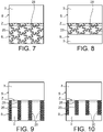
- Total recovery, case of figures 5, 6 and 7 , or partial, case of figures 8, 9 and 10 , of the surface S of a photovoltaic cell 3 must be chosen according to a double shading constraint and minimized resistive losses.
- Total coverage has the advantage of being simple to manufacture and of being uniform from an electrical point of view, but it entails a significant constraint on the shading.
- Partial covering has the advantage of reducing shading, but it entails electrical stress and thus requires covering more than the edge of each cell.
- the fraction of the surface S of each photovoltaic cell 3 covered by the interconnection element 20 is between 10 and 100%, in particular between 50 and 100%, and in particular also between 80 and 100%.
- the number of nodes 28 corresponding to the meeting place of at least two unit units 25, is between 2 and 50, and preferably between 5 and 15.
- Table 1 below presents values of certain parameters presented previously with two types of mesh of the interconnection element 20 (triangular and kagomé), using a cylindrical metal or metal alloy wire, in particular a copper wire covered by a coating with a low melting point of the SnBiAg type (alloys based on tin-bismuth-silver), the diameter of which is communicated (as a variant, it could also be a ribbon), and two types of photovoltaic cells 3 (cells of type III-V triple junction 4 ⁇ 8 cm 2 at 0.52 A and type Si, size M2, 15.675 ⁇ 15.675 mm 2 at 9.5A).
- interconnection elements 20 for example in the form of strips, as visible on the figures 9 and 10 . These bands can extend over the entire length of the surface S, as seen on the figure 9 , or even extend partially over the length of the surface S, as visible on the figure 10 . As a variant, it is also possible to use one or more strips in a central zone only, and not at the periphery of the surface S of each cell 3. In addition, it should be noted that the interconnection between two consecutive cells 3 can be carried out according to the direction of the length or the width of the cells 3.
- each interconnection element 20 may comprise an electrically conductive material in the form of one or more metals, such as copper or silver, and/or metal alloys, for example based on copper and silver. 'silver. These metals and/or alloys can be covered with a coating formed by a conductive metal alloy having a low melting temperature range, compatible with that of the lamination. Advantageously, it is then possible to weld and laminate in a single step. It should be noted that the notion of section of the interconnection element 20 corresponds to the section of the electrically conductive material, that of the possible coating being negligible.
- This low melting point coating can be formed by one or more metal alloys of the SnBiAg type (tin-bismuth-silver-based alloys), such as Sn 42 Bi 58 , Sn 64 Bi 35 Ag 1 , Sn 64.7 Bi 35 Ag 0.3 , Sn42Bis7.6Ago.4, Sn 42 Bi 57 Ag 1 , Sn 96.5 Ag 3.0 Cu 0.5 or even Sn 96.5 Ag 3.5 .
- SnBiAg type titanium-bismuth-silver-based alloys
- the electrically conductive material may be covered with an iron and nickel alloy coating, in particular of the Invar ® type (64% Fe, 36% Ni) or iron alloy, Nickel and Cobalt, in particular of the Kovar ® type (53.5% Fe, 29% Ni, 17% Co, 0.3% Mn, 0.2% Si, 0.02% C).
- an iron and nickel alloy coating in particular of the Invar ® type (64% Fe, 36% Ni) or iron alloy, Nickel and Cobalt, in particular of the Kovar ® type (53.5% Fe, 29% Ni, 17% Co, 0.3% Mn, 0.2% Si, 0.02% C).
- an interconnection element 20 according to the invention can be done by different approaches, and in particular: removal of material, 3D printing or weaving.
- This type of interconnection element 20 makes it possible to simplify the method of manufacturing the photovoltaic module 5 since the interconnection element(s) 20 are arranged at the same time as the cells 3 and do not require a welding step. The electrical connection is obtained during the lamination step.
- any type of photovoltaic cell 3 can be used in the context of the invention, including, for example, cells with rear face contact, or configurations of the “flip/flop” (“returned”) type, i.e. that is to say with an interconnection of consecutive bifacial cells (front face to front face, then rear face to rear face), or of the “shingle” (“tile”) type, that is to say with an interconnection of cells by partial covering), or of the “tilling/paving” type (“tiling/paving”), that is to say with an interconnection of cells with reduced spacing), among others.
Landscapes
- Photovoltaic Devices (AREA)
Applications Claiming Priority (1)
| Application Number | Priority Date | Filing Date | Title |
|---|---|---|---|
| FR2105947A FR3123762B1 (fr) | 2021-06-07 | 2021-06-07 | Elément d’interconnexion électrique d’au moins deux cellules photovoltaïques |
Publications (1)
| Publication Number | Publication Date |
|---|---|
| EP4102578A1 true EP4102578A1 (de) | 2022-12-14 |
Family
ID=76807840
Family Applications (1)
| Application Number | Title | Priority Date | Filing Date |
|---|---|---|---|
| EP22177283.3A Pending EP4102578A1 (de) | 2021-06-07 | 2022-06-03 | Elektrisches verbindungselement für mindestens zwei fotovoltaikzellen |
Country Status (2)
| Country | Link |
|---|---|
| EP (1) | EP4102578A1 (de) |
| FR (1) | FR3123762B1 (de) |
Citations (7)
| Publication number | Priority date | Publication date | Assignee | Title |
|---|---|---|---|---|
| EP1128445A2 (de) | 2000-02-23 | 2001-08-29 | The Boeing Company | Verbindungssystem für Solarzellen in der gleichen Ebene mit einer Lasche für eine integrierte Diode |
| WO2012081382A1 (ja) | 2010-12-15 | 2012-06-21 | 富士電機株式会社 | 太陽電池モジュールおよびインターコネクター材 |
| US20140352777A1 (en) * | 2011-12-07 | 2014-12-04 | NuvoSun, Inc. | Automated flexible solar cell fabrication and interconnection utilizing rolls expanded metallic mesh |
| US20170365557A1 (en) * | 2013-02-06 | 2017-12-21 | The Board Of Trustees Of The University Of Illinois | Self-similar and fractal design for stretchable electronics |
| CN109216188A (zh) * | 2018-09-07 | 2019-01-15 | 清华大学 | 柔性互连线及其制造方法以及参数测量方法 |
| EP3550615A1 (de) | 2018-04-04 | 2019-10-09 | SolAero Technologies Corp. | Verbindungselement |
| CN109573939B (zh) * | 2018-10-24 | 2020-11-17 | 永康国科康复工程技术有限公司 | 双层应变基体及可拉伸电子器件 |
-
2021
- 2021-06-07 FR FR2105947A patent/FR3123762B1/fr active Active
-
2022
- 2022-06-03 EP EP22177283.3A patent/EP4102578A1/de active Pending
Patent Citations (7)
| Publication number | Priority date | Publication date | Assignee | Title |
|---|---|---|---|---|
| EP1128445A2 (de) | 2000-02-23 | 2001-08-29 | The Boeing Company | Verbindungssystem für Solarzellen in der gleichen Ebene mit einer Lasche für eine integrierte Diode |
| WO2012081382A1 (ja) | 2010-12-15 | 2012-06-21 | 富士電機株式会社 | 太陽電池モジュールおよびインターコネクター材 |
| US20140352777A1 (en) * | 2011-12-07 | 2014-12-04 | NuvoSun, Inc. | Automated flexible solar cell fabrication and interconnection utilizing rolls expanded metallic mesh |
| US20170365557A1 (en) * | 2013-02-06 | 2017-12-21 | The Board Of Trustees Of The University Of Illinois | Self-similar and fractal design for stretchable electronics |
| EP3550615A1 (de) | 2018-04-04 | 2019-10-09 | SolAero Technologies Corp. | Verbindungselement |
| CN109216188A (zh) * | 2018-09-07 | 2019-01-15 | 清华大学 | 柔性互连线及其制造方法以及参数测量方法 |
| CN109573939B (zh) * | 2018-10-24 | 2020-11-17 | 永康国科康复工程技术有限公司 | 双层应变基体及可拉伸电子器件 |
Non-Patent Citations (7)
| Title |
|---|
| JO MANSIK ET AL: "3D Printer-Based Encapsulated Origami Electronics for Extreme System Stretchability and High Areal Coverage", ACS NANO, vol. 13, no. 11, 4 October 2019 (2019-10-04), US, pages 12500 - 12510, XP055884689, ISSN: 1936-0851, DOI: 10.1021/acsnano.9b02362 * |
| JO MANSIK ET AL: "Supporting Information (3D Printer-Based Encapsulated Origami Electronics for Extreme System Stretchability and High Areal Coverage)", ACS NANO, vol. 13, no. 11, 4 October 2019 (2019-10-04), US, pages 1 - 45, XP055888189, ISSN: 1936-0851, DOI: 10.1021/acsnano.9b02362 * |
| JONGSEUNG YOON ET AL: "Ultrathin silicon solar microcells for semitransparent, mechanically flexible and microconcentrator module designs", NATURE MATERIALS, vol. 7, no. 11, 5 October 2008 (2008-10-05), London, pages 907 - 915, XP055276191, ISSN: 1476-1122, DOI: 10.1038/nmat2287 * |
| MUSA T. ZARMAI ET AL.: "School of Engineering, Faculty of Science and Engineering", vol. 154, 15 September 2015, UNIVERSITY OF WOLVERHAMPTON, article "A review of interconnection technologies for improved crystalline silicon solar cell photovoltaic module assembly", pages: 173 - 182 |
| SU YEWANG ET AL: "In-Plane Deformation Mechanics for Highly Stretchable Electronics", ADVANCED MATERIALS, vol. 29, no. 8, 1604989, 22 December 2016 (2016-12-22), DE, pages 1 - 12, XP055885171, ISSN: 0935-9648, DOI: 10.1002/adma.201604989 * |
| SU YEWANG ET AL: "Supporting Information (In-Plane Deformation Mechanics for Highly Stretchable Electronics)", ADVANCED MATERIALS, vol. 29, no. 8, 1604989, 22 December 2016 (2016-12-22), DE, pages 1 - 26, XP055885945, ISSN: 0935-9648, DOI: 10.1002/adma.201604989 * |
| ZHANG YIHUI ET AL: "A hierarchical computational model for stretchable interconnects with fractal-inspired designs", JOURNAL OF THE MECHANICS AND PHYSICS OF SOLIDS., vol. 72, 12 August 2014 (2014-08-12), GB, pages 115 - 130, XP055885167, ISSN: 0022-5096, DOI: 10.1016/j.jmps.2014.07.011 * |
Also Published As
| Publication number | Publication date |
|---|---|
| FR3123762A1 (fr) | 2022-12-09 |
| FR3123762B1 (fr) | 2024-05-31 |
Similar Documents
| Publication | Publication Date | Title |
|---|---|---|
| JP5629010B2 (ja) | 改良された光起電力セルアセンブリ及び方法 | |
| CN104412357B (zh) | 积体薄膜太阳能晶胞电池的互连 | |
| EP2833416B1 (de) | Solarzellenmodul mit rückseitenkontakt | |
| EP2510553B1 (de) | Pv-zelle, verfahren zur montage mehrerer zellen und anordnung aus mehreren pv-zellen | |
| EP3493277B1 (de) | Verfahren zur verbindung von photovoltaikzellen mit einer elektrode, ausgestattet mit metallnanodrähten | |
| EP4002491B1 (de) | Verbessertes leichtes und flexibles fotovoltaikmodul | |
| FR2922366A1 (fr) | Perfectionnements apportes a des elements capables de collecter de la lumiere | |
| WO2016198797A1 (fr) | Module photovoltaique et procede d'interconnexion de cellules photovoltaiques pour fabriquer un tel module | |
| WO2006045968A1 (fr) | Structure multicouche monolithique pour la connexion de cellules a semi-conducteur | |
| EP2981156B1 (de) | Fotovoltaikpaneel und ein herstellungsverfahren eines solchen paneels | |
| EP3496160A1 (de) | Fotovoltaikmodul, das fotovoltaikzellen umfasst, die mithilfe von verbindungselementen miteinander verbunden sind | |
| FR2945670A1 (fr) | Dispositif photovoltaique et procede de fabrication | |
| EP4102578A1 (de) | Elektrisches verbindungselement für mindestens zwei fotovoltaikzellen | |
| EP3809473A1 (de) | Verfahren zum verbindung von fotovoltaik-zellen durch metalldrähte in kontakt mit lötpasten-pads | |
| WO2023073308A1 (fr) | Procédé de fabrication d'un assemblage d'une cellule photovoltaïque et d'un élément d'interconnexion | |
| EP4356435A1 (de) | Photovoltaischer string | |
| EP4701374A1 (de) | Vorrichtung zur verbindung von photovoltaischen zellen | |
| WO2010070573A2 (fr) | Structure d'un module photovoltaïque | |
| EP4701373A1 (de) | Vorrichtung zur verbindung von photovoltaischen zellen | |
| FR3165634A1 (fr) | Masque de tir laser pour l’interconnexion de cellules photovoltaïques | |
| WO2016096669A1 (fr) | Dispositif photovoltaique doté d'une couche conductrice et transparente a base de nanofils et procédé de fabrication d'un tel dispositif | |
| EP4416764A1 (de) | Anordnung für ein photovoltaikmodul, photovoltaikmodul und verfahren zur herstellung der anordnung und des moduls | |
| FR3116651A1 (fr) | Procédé de fabrication d’un module photovoltaïque léger et flexible intégrant une protection thermique | |
| WO2025083030A1 (fr) | Module photovoltaïque a connexions integrees d'assemblage en serie et en parallele | |
| WO2025114369A1 (fr) | Cellule photovoltaïque ameliorée comprenant une interface de connexion |
Legal Events
| Date | Code | Title | Description |
|---|---|---|---|
| PUAI | Public reference made under article 153(3) epc to a published international application that has entered the european phase |
Free format text: ORIGINAL CODE: 0009012 |
|
| STAA | Information on the status of an ep patent application or granted ep patent |
Free format text: STATUS: REQUEST FOR EXAMINATION WAS MADE |
|
| 17P | Request for examination filed |
Effective date: 20220603 |
|
| AK | Designated contracting states |
Kind code of ref document: A1 Designated state(s): AL AT BE BG CH CY CZ DE DK EE ES FI FR GB GR HR HU IE IS IT LI LT LU LV MC MK MT NL NO PL PT RO RS SE SI SK SM TR |
|
| RAP3 | Party data changed (applicant data changed or rights of an application transferred) |
Owner name: COMMISSARIAT A L'ENERGIE ATOMIQUE ET AUX ENERGIESALTERNATIVES |