EP4102677B1 - Ladegerät, steuerverfahren dafür und ladesystem - Google Patents
Ladegerät, steuerverfahren dafür und ladesystem Download PDFInfo
- Publication number
- EP4102677B1 EP4102677B1 EP21785177.3A EP21785177A EP4102677B1 EP 4102677 B1 EP4102677 B1 EP 4102677B1 EP 21785177 A EP21785177 A EP 21785177A EP 4102677 B1 EP4102677 B1 EP 4102677B1
- Authority
- EP
- European Patent Office
- Prior art keywords
- voltage
- charging
- controller
- electrically connected
- phase
- Prior art date
- Legal status (The legal status is an assumption and is not a legal conclusion. Google has not performed a legal analysis and makes no representation as to the accuracy of the status listed.)
- Active
Links
Images


Classifications
-
- H—ELECTRICITY
- H02—GENERATION; CONVERSION OR DISTRIBUTION OF ELECTRIC POWER
- H02J—ELECTRIC POWER NETWORKS; CIRCUIT ARRANGEMENTS OR SYSTEMS FOR SUPPLYING OR DISTRIBUTING ELECTRIC POWER; SYSTEMS FOR STORING ELECTRIC ENERGY
- H02J7/00—Circuit arrangements for charging or discharging batteries or for supplying loads from batteries
- H02J7/02—Circuit arrangements for charging or discharging batteries or for supplying loads from batteries for charging batteries from AC mains by converters
- H02J7/04—Regulation of charging current or voltage
- H02J7/06—Regulation of charging current or voltage using discharge tubes or semiconductor devices
-
- H—ELECTRICITY
- H02—GENERATION; CONVERSION OR DISTRIBUTION OF ELECTRIC POWER
- H02J—ELECTRIC POWER NETWORKS; CIRCUIT ARRANGEMENTS OR SYSTEMS FOR SUPPLYING OR DISTRIBUTING ELECTRIC POWER; SYSTEMS FOR STORING ELECTRIC ENERGY
- H02J7/00—Circuit arrangements for charging or discharging batteries or for supplying loads from batteries
- H02J7/02—Circuit arrangements for charging or discharging batteries or for supplying loads from batteries for charging batteries from AC mains by converters
-
- H—ELECTRICITY
- H01—ELECTRIC ELEMENTS
- H01M—PROCESSES OR MEANS, e.g. BATTERIES, FOR THE DIRECT CONVERSION OF CHEMICAL ENERGY INTO ELECTRICAL ENERGY
- H01M10/00—Secondary cells; Manufacture thereof
- H01M10/42—Methods or arrangements for servicing or maintenance of secondary cells or secondary half-cells
- H01M10/44—Methods for charging or discharging
-
- H—ELECTRICITY
- H02—GENERATION; CONVERSION OR DISTRIBUTION OF ELECTRIC POWER
- H02J—ELECTRIC POWER NETWORKS; CIRCUIT ARRANGEMENTS OR SYSTEMS FOR SUPPLYING OR DISTRIBUTING ELECTRIC POWER; SYSTEMS FOR STORING ELECTRIC ENERGY
- H02J7/00—Circuit arrangements for charging or discharging batteries or for supplying loads from batteries
- H02J7/60—Circuit arrangements for charging or discharging batteries or for supplying loads from batteries including safety or protection arrangements
-
- H—ELECTRICITY
- H02—GENERATION; CONVERSION OR DISTRIBUTION OF ELECTRIC POWER
- H02M—APPARATUS FOR CONVERSION BETWEEN AC AND AC, BETWEEN AC AND DC, OR BETWEEN DC AND DC, AND FOR USE WITH MAINS OR SIMILAR POWER SUPPLY SYSTEMS; CONVERSION OF DC OR AC INPUT POWER INTO SURGE OUTPUT POWER; CONTROL OR REGULATION THEREOF
- H02M1/00—Details of apparatus for conversion
- H02M1/32—Means for protecting converters other than automatic disconnection
-
- H—ELECTRICITY
- H02—GENERATION; CONVERSION OR DISTRIBUTION OF ELECTRIC POWER
- H02M—APPARATUS FOR CONVERSION BETWEEN AC AND AC, BETWEEN AC AND DC, OR BETWEEN DC AND DC, AND FOR USE WITH MAINS OR SIMILAR POWER SUPPLY SYSTEMS; CONVERSION OF DC OR AC INPUT POWER INTO SURGE OUTPUT POWER; CONTROL OR REGULATION THEREOF
- H02M3/00—Conversion of DC power input into DC power output
- H02M3/22—Conversion of DC power input into DC power output with intermediate conversion into AC
- H02M3/24—Conversion of DC power input into DC power output with intermediate conversion into AC by static converters
- H02M3/28—Conversion of DC power input into DC power output with intermediate conversion into AC by static converters using discharge tubes with control electrode or semiconductor devices with control electrode to produce the intermediate AC
- H02M3/325—Conversion of DC power input into DC power output with intermediate conversion into AC by static converters using discharge tubes with control electrode or semiconductor devices with control electrode to produce the intermediate AC using devices of a triode or a transistor type requiring continuous application of a control signal
- H02M3/335—Conversion of DC power input into DC power output with intermediate conversion into AC by static converters using discharge tubes with control electrode or semiconductor devices with control electrode to produce the intermediate AC using devices of a triode or a transistor type requiring continuous application of a control signal using semiconductor devices only
- H02M3/33507—Conversion of DC power input into DC power output with intermediate conversion into AC by static converters using discharge tubes with control electrode or semiconductor devices with control electrode to produce the intermediate AC using devices of a triode or a transistor type requiring continuous application of a control signal using semiconductor devices only with automatic control of the output voltage or current, e.g. flyback converters
-
- H—ELECTRICITY
- H02—GENERATION; CONVERSION OR DISTRIBUTION OF ELECTRIC POWER
- H02M—APPARATUS FOR CONVERSION BETWEEN AC AND AC, BETWEEN AC AND DC, OR BETWEEN DC AND DC, AND FOR USE WITH MAINS OR SIMILAR POWER SUPPLY SYSTEMS; CONVERSION OF DC OR AC INPUT POWER INTO SURGE OUTPUT POWER; CONTROL OR REGULATION THEREOF
- H02M3/00—Conversion of DC power input into DC power output
- H02M3/22—Conversion of DC power input into DC power output with intermediate conversion into AC
- H02M3/24—Conversion of DC power input into DC power output with intermediate conversion into AC by static converters
- H02M3/28—Conversion of DC power input into DC power output with intermediate conversion into AC by static converters using discharge tubes with control electrode or semiconductor devices with control electrode to produce the intermediate AC
- H02M3/325—Conversion of DC power input into DC power output with intermediate conversion into AC by static converters using discharge tubes with control electrode or semiconductor devices with control electrode to produce the intermediate AC using devices of a triode or a transistor type requiring continuous application of a control signal
- H02M3/335—Conversion of DC power input into DC power output with intermediate conversion into AC by static converters using discharge tubes with control electrode or semiconductor devices with control electrode to produce the intermediate AC using devices of a triode or a transistor type requiring continuous application of a control signal using semiconductor devices only
- H02M3/33569—Conversion of DC power input into DC power output with intermediate conversion into AC by static converters using discharge tubes with control electrode or semiconductor devices with control electrode to produce the intermediate AC using devices of a triode or a transistor type requiring continuous application of a control signal using semiconductor devices only having several active switching elements
-
- H—ELECTRICITY
- H02—GENERATION; CONVERSION OR DISTRIBUTION OF ELECTRIC POWER
- H02M—APPARATUS FOR CONVERSION BETWEEN AC AND AC, BETWEEN AC AND DC, OR BETWEEN DC AND DC, AND FOR USE WITH MAINS OR SIMILAR POWER SUPPLY SYSTEMS; CONVERSION OF DC OR AC INPUT POWER INTO SURGE OUTPUT POWER; CONTROL OR REGULATION THEREOF
- H02M7/00—Conversion of AC power input into DC power output; Conversion of DC power input into AC power output
- H02M7/02—Conversion of AC power input into DC power output without possibility of reversal
- H02M7/04—Conversion of AC power input into DC power output without possibility of reversal by static converters
- H02M7/06—Conversion of AC power input into DC power output without possibility of reversal by static converters using discharge tubes without control electrode or semiconductor devices without control electrode
-
- H—ELECTRICITY
- H01—ELECTRIC ELEMENTS
- H01M—PROCESSES OR MEANS, e.g. BATTERIES, FOR THE DIRECT CONVERSION OF CHEMICAL ENERGY INTO ELECTRICAL ENERGY
- H01M2220/00—Batteries for particular applications
- H01M2220/30—Batteries in portable systems, e.g. mobile phone, laptop
-
- H—ELECTRICITY
- H02—GENERATION; CONVERSION OR DISTRIBUTION OF ELECTRIC POWER
- H02J—ELECTRIC POWER NETWORKS; CIRCUIT ARRANGEMENTS OR SYSTEMS FOR SUPPLYING OR DISTRIBUTING ELECTRIC POWER; SYSTEMS FOR STORING ELECTRIC ENERGY
- H02J2207/00—Details of circuit arrangements for charging or discharging batteries or supplying loads from batteries
- H02J2207/20—Charging or discharging characterised by the power electronics converter
-
- H—ELECTRICITY
- H02—GENERATION; CONVERSION OR DISTRIBUTION OF ELECTRIC POWER
- H02J—ELECTRIC POWER NETWORKS; CIRCUIT ARRANGEMENTS OR SYSTEMS FOR SUPPLYING OR DISTRIBUTING ELECTRIC POWER; SYSTEMS FOR STORING ELECTRIC ENERGY
- H02J7/00—Circuit arrangements for charging or discharging batteries or for supplying loads from batteries
- H02J7/60—Circuit arrangements for charging or discharging batteries or for supplying loads from batteries including safety or protection arrangements
- H02J7/64—Circuit arrangements for charging or discharging batteries or for supplying loads from batteries including safety or protection arrangements against overvoltage
-
- H—ELECTRICITY
- H02—GENERATION; CONVERSION OR DISTRIBUTION OF ELECTRIC POWER
- H02M—APPARATUS FOR CONVERSION BETWEEN AC AND AC, BETWEEN AC AND DC, OR BETWEEN DC AND DC, AND FOR USE WITH MAINS OR SIMILAR POWER SUPPLY SYSTEMS; CONVERSION OF DC OR AC INPUT POWER INTO SURGE OUTPUT POWER; CONTROL OR REGULATION THEREOF
- H02M1/00—Details of apparatus for conversion
- H02M1/0003—Details of control, feedback or regulation circuits
- H02M1/0006—Arrangements for supplying an adequate voltage to the control circuit of converters
-
- Y—GENERAL TAGGING OF NEW TECHNOLOGICAL DEVELOPMENTS; GENERAL TAGGING OF CROSS-SECTIONAL TECHNOLOGIES SPANNING OVER SEVERAL SECTIONS OF THE IPC; TECHNICAL SUBJECTS COVERED BY FORMER USPC CROSS-REFERENCE ART COLLECTIONS [XRACs] AND DIGESTS
- Y02—TECHNOLOGIES OR APPLICATIONS FOR MITIGATION OR ADAPTATION AGAINST CLIMATE CHANGE
- Y02E—REDUCTION OF GREENHOUSE GAS [GHG] EMISSIONS, RELATED TO ENERGY GENERATION, TRANSMISSION OR DISTRIBUTION
- Y02E60/00—Enabling technologies; Technologies with a potential or indirect contribution to GHG emissions mitigation
- Y02E60/10—Energy storage using batteries
Definitions
- This application relates to the field of terminal device charging technologies, and in particular, to a charging apparatus, a charging apparatus control method, and a charging system.
- a relatively large quantity of half bridges are used in the charging apparatus field, such as an active clamp flyback (Active clamp flyback, ACF) topology.
- ACF active clamp flyback
- a voltage of a clamp capacitor in the half-bridge circuit structure is excessively high because an upper bridge switch is not turned on, and the voltage of the clamp capacitor exceeds a voltage withstand value of the clamp capacitor.
- CN108988652A discloses a flyback active clamp circuit and control method.
- US20200091826A1 discloses a control circuit for a flyback converter configured to adjust a conduction time of an auxiliary switch of the converter.
- Embodiments of this application provide a charging apparatus, a charging apparatus control method, and a charging system, to avoid problems such as a short circuit or an open circuit that occurs when a voltage of a clamp capacitor is excessively high.
- a charging apparatus configured to supply power to a load.
- the charging apparatus includes a rectifier circuit, a transformer, a lower bridge switch, a clamp capacitor, and an upper bridge switch.
- the rectifier circuit is configured to rectify a received alternating current.
- the transformer is configured to buck an output voltage of the rectifier circuit and then provide a bucked output voltage to the load.
- the transformer includes a primary coil and at least one secondary coil, and a first end of the primary coil is electrically connected to the rectifier circuit.
- a first end of the lower bridge switch is electrically connected to a second end of the primary coil, and a second end of the lower bridge switch is electrically connected to a grounding end.
- the lower bridge switch is configured to be turned on in a first phase of a charging cycle of the charging apparatus, so that a current output by the rectifier circuit is transmitted to the primary coil, to charge the primary coil.
- a first end of the clamp capacitor is electrically connected to the first end of the primary coil.
- a first end of the upper bridge switch is electrically connected to a second end of the clamp capacitor.
- a second end of the upper bridge switch is electrically connected to the second end of the primary coil.
- the upper bridge switch is configured to be turned on in a second phase of the charging cycle, so that a leakage inductance in the primary coil charges the clamp capacitor, and the clamp capacitor discharges electricity to the primary coil.
- the charging apparatus further includes a controller.
- the processor is configured to control, in the first phase and the second phase, the upper bridge switch and the lower bridge switch to be alternatively turned on.
- the controller is further configured to: when the lower bridge switch is turned off, obtain a sampling waveform at a location at which the controller is electrically connected to the transformer; and when the sampling waveform in a current charging cycle is abnormal, turn off the lower bridge switch in a first phase of a next charging cycle.
- the sampling waveform includes a voltage waveform of the primary coil or a voltage waveform of the secondary coil. In this way, the leakage inductance in the primary coil is prevented from charging the clamp capacitor, thereby avoiding problems such as a short circuit or an open circuit that occurs when a voltage of the clamp capacitor is excessively high.
- the location at which the controller is electrically connected to the transformer is between the second end of the primary coil and the first end of the lower bridge switch, or between the second end of the upper bridge switch and the first end of the lower bridge switch.
- a voltage value of Vds is tested when the lower bridge switch is turned off, to determine whether the sampling waveform is an abnormal waveform.
- the transformer includes a first secondary coil, and the transformer further includes a first rectifier diode.
- a first end of the first secondary coil is electrically connected to an anode of the first rectifier diode, a cathode of the first rectifier diode is configured to be electrically connected to the load, and a second end of the first secondary coil is grounded.
- the first secondary coil and the primary coil are configured to buck a voltage of the primary coil through electromagnetic induction, and generate a first output voltage.
- a sampling point at the location at which the controller is electrically connected to the transformer is at the first end of the first secondary coil.
- a voltage waveform of the first output voltage is synchronous with the voltage waveform of the primary coil. Therefore, when the lower bridge switch is turned off, a waveform graph of the first output voltage may be collected to determine whether the sampling waveform is an abnormal waveform.
- the charging apparatus further includes a power supply circuit.
- the power supply circuit is electrically connected to the controller and configured to supply power to the controller.
- the transformer further includes a second secondary coil and a second rectifier diode. A first end of the second secondary coil is electrically connected to an anode of the second rectifier diode, a cathode of the second rectifier diode is electrically connected to the power supply circuit, and a second electrode of the second secondary coil is grounded. Based on this, the second secondary coil and the primary coil are configured to buck the voltage of the primary coil through electromagnetic induction, and generate a second output voltage, where the second output voltage is used to supply power to the power supply circuit.
- the location at which the controller is electrically connected to the transformer is at the first end of the second secondary coil.
- a voltage waveform of the second output voltage is synchronous with the voltage waveform of the primary coil. Therefore, when the lower bridge switch is turned off, a waveform graph of the second output voltage may be collected to determine whether the sampling waveform is an abnormal waveform.
- the sampling waveform in a current charging cycle is abnormal includes: The controller obtains a platform voltage Vt of the sampling waveform in a second phase of the N th charging cycle, and detects, in the second phase, that a peak voltage Vp of the sampling waveform is greater than the platform voltage Vt; or calculates, in the second phase, an integral area S, in the second phase, that is of a part of the sampling waveform and that exceeds the platform voltage Vt, where S > 0. N ⁇ 1 and N is a positive integer.
- the peak voltage Vp becomes larger than the platform voltage Vt. Therefore, Vp in a same cycle or an area of a part exceeding the platform voltage may be detected to determine whether the sampling waveform is an abnormal waveform.
- the sampling waveform in a current charging cycle is abnormal includes: The controller obtains a platform voltage Vt of the sampling waveform in a second phase of the N th charging cycle, continuously obtains an integral area S that is in the second phase and that is of a part exceeding the platform voltage Vt in the second phase of the N th charging cycle and in a second phase of each of M charging cycles before the N th charging cycle, and calculates an area difference ⁇ S between integral areas S that are in two adjacent charging cycles and that are in the (M + 1) integral areas S, where ⁇ S # 0. N ⁇ 1, and N is a positive number. M ⁇ 1, and M is a positive number.
- the peak voltage Vp becomes larger than the platform voltage Vt. Therefore, areas of parts exceeding the platform voltage in different cycles may be detected to determine whether the sampling waveform is an abnormal waveform.
- the sampling waveform in a current charging cycle is abnormal includes: The controller obtains a platform voltage Vt of the sampling waveform in a second phase of the (N - 1) th charging cycle, and obtains a peak voltage Vp of the sampling waveform in a second phase of the N th charging cycle, where Vp > Vt. N ⁇ 2, and N is a positive integer.
- the peak voltage Vp becomes larger than the platform voltage Vt. Therefore, Vt in a current cycle and Vp in a next cycle may be detected to determine whether the sampling waveform is an abnormal waveform.
- Vo is the output voltage of the rectifier circuit
- Vo 1 is the output voltage provided by the transformer to the load
- T1 is a ratio of a quantity of turns of the primary coil in the transformer to a quantity of turns of the secondary coil configured to supply power to the load.
- T2 is a ratio of a quantity of turns of the primary coil in the transformer to a quantity of turns of the secondary coil electrically connected to the controller. In this way, an abnormal waveform may be determined by using a value of the platform voltage.
- the sampling waveform in a current charging cycle is abnormal includes: The controller continuously obtains a peak voltage Vp of the sampling waveform in a second phase of the N th charging cycle and in a second phase of each of M charging cycles before the N th charging cycle, and calculates a voltage difference ⁇ V between peak voltages Vp of the sampling waveform that are in two adjacent charging cycles and that are in the (M + 1) peak voltages Vp, where ⁇ V # 0. N ⁇ 1, and N is a positive number. M ⁇ 1, and M is a positive number.
- a peak voltage value of an abnormal waveform is different from a peak voltage value of a normal waveform. Therefore, peak voltages Vp in different cycles may be calculated to determine whether the sampling waveform is an abnormal waveform.
- the sampling waveform in a current charging cycle is abnormal includes: The controller learns that a voltage of the sampling waveform is greater than or equal to 30 V at an end of a third phase of the N th charging cycle.
- N ⁇ 1 and N is a positive integer.
- the voltage at the end of the third phase of the N th charging cycle that is, a voltage at a start end of a first phase of the (N + 1) th cycle, generates a negative current at a location of the primary coil because the upper bridge switch is turned on. Under action of the current, power in a parasitic capacitor in the lower bridge switch is removed, so that the voltage value rapidly drops to 0 or approaches 0.
- the upper bridge switch is turned off, and the negative current does not exist, so that the voltage at the end of the third phase of the N th charging cycle is relatively high. Therefore, the voltage value at the end of the third phase of the N th charging cycle may be detected to determine whether the sampling waveform in the current charging cycle is an abnormal waveform.
- the charging apparatus further includes a sampling circuit, and the sampling circuit is electrically connected between the controller and the transformer.
- the sampling circuit is configured to buck a voltage at a location at which the sampling circuit is electrically connected to the transformer and then provide a bucked voltage to the controller. In this way, it may be ensured that a voltage value at the location at which the sampling circuit is electrically connected to the transformer does not exceed a voltage withstand value of the controller.
- the sampling circuit includes a first resistor and a second resistor, and a first end of the first resistor is electrically connected to the transformer.
- a first end of the second resistor is electrically connected to a second end of the first resistor and the controller, and a second end of the second resistor is grounded.
- a voltage value collected by the controller may be changed by adjusting a ratio of a resistance value of the first resistor to a resistance value of the second resistor, to ensure that the voltage value does not exceed a voltage withstand value of the controller.
- the ratio of the resistance value of the first resistor to the resistance value of the second resistor is larger, the collected voltage value is smaller.
- the sampling circuit includes a first coil and a second coil.
- a first end of the first coil is electrically connected to the transformer, and a second end of the first coil is grounded.
- a first end of the second coil is electrically connected to the controller, and the other end of the second coil is grounded.
- a quantity of turns of the first coil is greater than a quantity of turns of the second coil.
- the voltage value collected by the controller may be changed by controlling a ratio of the quantity of turns of the first coil to the quantity of turns of the second coil. When the ratio of the quantity of turns of the first coil to the quantity of turns of the second coil is larger, the collected voltage value is smaller.
- the sampling circuit includes a third resistor and a second capacitor.
- a first end of the third resistor is electrically connected to the controller, and a second end of the third resistor is grounded.
- a first end of the second capacitor is electrically connected to the transformer, and a second end of the second capacitor is electrically connected to the controller.
- the voltage value collected by the controller may be changed by adjusting a capacitance value of the second capacitor or a resistance value of the third resistor. When the capacitance value of the second capacitor or the resistance value of the third resistor is larger, the collected voltage value is larger.
- a charging system includes an electronic device and any one of the foregoing charging apparatuses.
- the electronic device includes a battery, and the battery is electrically connected to the charging apparatus.
- a charging apparatus control method is provided, and the charging apparatus control method is applied to a charging apparatus.
- the charging apparatus includes a rectifier circuit, a transformer, a lower bridge switch, a clamp capacitor, an upper bridge switch, and a controller.
- the transformer includes a primary coil and at least one secondary coil, and a first end of the primary coil is electrically connected to the rectifier circuit.
- the controller is electrically connected to the transformer.
- a first end of the lower bridge switch is electrically connected to a second end of the primary coil, and a second end of the lower bridge switch is electrically connected to a grounding end.
- a first end of the clamp capacitor is electrically connected to the first end of the primary coil.
- the charging apparatus control method includes: In a first phase of a charging cycle of the charging apparatus, the controller controls the lower bridge switch to be turned on and the upper bridge switch to be turned off, so that a current output by the rectifier circuit charges the primary coil. In a second phase of the charging cycle, the controller controls the lower bridge switch to be turned off and the upper bridge switch to be turned on, so that the primary coil discharges electricity, the transformer bucks an output voltage of the rectifier circuit and provides a bucked output voltage to a load, and a leakage inductance in the primary coil charges the clamp capacitor.
- the charging apparatus control method further includes a waveform processing step: In the second phase of the charging cycle, the controller obtains a sampling waveform at a location at which the controller is electrically connected to the transformer, where the sampling waveform includes a voltage waveform of the primary coil or a voltage waveform of the secondary coil.
- the controller turns off the lower bridge switch in a first phase of a next charging cycle.
- the sampling waveform in a current charging cycle is abnormal includes: The controller obtains a platform voltage Vt of the sampling waveform in a second phase of the N th charging cycle, and detects, in the second phase, that a peak voltage Vp of the sampling waveform is greater than the platform voltage Vt; or calculates, in the second phase, an integral area S, in the second phase, that is of a part of the sampling waveform and that exceeds the platform voltage Vt, where S > 0. N ⁇ 1 and N is a positive integer.
- the peak voltage Vp becomes larger than the platform voltage Vt. Therefore, Vp in a same cycle or an area of a part exceeding the platform voltage may be detected to determine whether the sampling waveform is an abnormal waveform.
- the sampling waveform in a current charging cycle is abnormal includes: The controller obtains a platform voltage Vt of the sampling waveform in a second phase of the N th charging cycle, continuously obtains an integral area S that is in the second phase and that is of a part exceeding the platform voltage Vt in the second phase of the N th charging cycle and in a second phase of each of M charging cycles before the N th charging cycle, and calculates an area difference ⁇ S between integral areas S that are in two adjacent charging cycles and that are in the (M + 1) integral areas S, where ⁇ S # 0. N ⁇ 1, and N is a positive number. M ⁇ 1, and M is a positive number.
- the peak voltage Vp becomes larger than the platform voltage Vt. Therefore, areas of parts exceeding the platform voltage in different cycles may be detected to determine whether the sampling waveform is an abnormal waveform.
- the sampling waveform in a current charging cycle is abnormal includes: The controller obtains a platform voltage Vt of the sampling waveform in a second phase of the (N - 1) th charging cycle, and obtains a peak voltage Vp of the sampling waveform in a second phase of the N th charging cycle, where Vp > Vt. N ⁇ 2, and N is a positive integer.
- the peak voltage Vp becomes larger than the platform voltage Vt. Therefore, Vt in a current cycle and Vp in a next cycle may be detected to determine whether the sampling waveform is an abnormal waveform.
- Vo is the output voltage of the rectifier circuit
- Vo 1 is the output voltage provided by the transformer to the load
- T1 is a ratio of a quantity of turns of the primary coil in the transformer to a quantity of turns of the secondary coil configured to supply power to the load.
- T2 is a ratio of a quantity of turns of the primary coil in the transformer to a quantity of turns of the secondary coil electrically connected to the controller. In this way, an abnormal waveform may be determined by using a value of the platform voltage.
- the sampling waveform in a current charging cycle is abnormal includes: The controller continuously obtains a peak voltage Vp of the sampling waveform in a second phase of the N th charging cycle and in a second phase of each of M charging cycles before the N th charging cycle, and calculates a voltage difference ⁇ V between peak voltages Vp of the sampling waveform that are in two adjacent charging cycles and that are in the (M + 1) peak voltages Vp, where ⁇ V # 0. N ⁇ 1, and N is a positive number. M ⁇ 1, and M is a positive number.
- a peak voltage value of an abnormal waveform is different from a peak voltage value of a normal waveform. Therefore, peak voltages Vp in different cycles may be calculated to determine whether the sampling waveform is an abnormal waveform.
- the sampling waveform in a current charging cycle is abnormal includes: The controller learns that a voltage of the sampling waveform is greater than or equal to 30 V at an end of a third phase of the N th charging cycle.
- N ⁇ 1 and N is a positive integer.
- the voltage at the end of the third phase of the N th charging cycle that is, a voltage at a start end of a first phase of the (N + 1) th cycle, generates a negative current at a location of the primary coil because the upper bridge switch is turned on. Under action of the current, power in a parasitic capacitor in the lower bridge switch is removed, so that the voltage value rapidly drops to 0 or approaches 0.
- the upper bridge switch is turned off, and the negative current does not exist, so that the voltage at the end of the third phase of the N th charging cycle is relatively high. Therefore, the voltage value at the end of the third phase of the N th charging cycle may be detected to determine whether the sampling waveform in the current charging cycle is an abnormal waveform.
- first”, “second”, and the like are merely intended for a purpose of description, and shall not be understood as an indication or implication of relative importance or implicit indication of a quantity of indicated technical features. Therefore, a feature limited by “first”, “second”, or the like may explicitly or implicitly include one or more features. In the description of this application, unless otherwise stated, "a plurality of" means two or more than two.
- orientation terms such as “left” and “right” may include but are not limited to orientations of components schematically placed in the accompanying drawings. It should be understood that these orientation terms are relative concepts and are used for relative description and clarification, and may correspondingly change based on a change of an orientation of a component placed in the accompanying drawings.
- connection may be a fixed connection, a detachable connection, or an integrated connection; and may be a direct connection, or an indirect connection by an intermediate medium.
- coupling may be a manner of an electrical connection for implementing signal transmission. The “coupling” may be a direct electrical connection, or may be an indirect electrical connection by an intermediate medium.
- the charging system may include an electronic device 01 and a charging apparatus 02.
- the electronic device 01 may include a mobile phone, a tablet computer, a computer, a smart watch, a camera, and the like. This is not limited in this application.
- a battery 102 in the electronic device 01 is connected to a connector 101, a first power supply interface 301, and a second power supply interface 302, to be electrically connected to the charging apparatus 02.
- the charging apparatus 02 accesses a 220 V alternating current, converts the alternating current into a direct current that is suitable for working of the electronic device 01, so as to charge the battery 102 in the electronic device 01.
- the battery 102 supplies required power to a load circuit electrically connected to the battery 102 in the electronic device 01, so as to implement normal operation of the electronic device 01.
- the charging apparatus 02 may include a rectifier circuit 201 and a transformer 202.
- the rectifier circuit 201 is electrically connected to the transformer 202, and a right side of the transformer 202 is electrically connected to a load 0 1.
- the rectifier circuit 201 is configured to rectify a received alternating current, and provide a voltage to the transformer 202.
- the transformer 202 is configured to convert the voltage into a working voltage applicable to the load 01, and transmit the voltage to the load 01. Therefore, the transformer 202 provides a voltage bucking function.
- the rectifier circuit 201 may be electrically connected to an external power supply network by using a live wire (live wire, L) and a neutral wire (neutral wire, N), so as to rectify an accessed alternating current.
- the rectifier circuit 201 may include a full-bridge rectifier circuit FB and a capacitor Cst.
- the accessed 220 V alternating current flows through the full-bridge rectifier circuit FB, and then the alternating current is converted into a direct current, and the direct current is stored in the capacitor Cst.
- the capacitor Cst is configured to provide a voltage to the transformer 202 electrically connected to the capacitor Cst.
- the voltage is referred to as an output voltage Vo of the rectifier circuit 201.
- the transformer 202 may include a primary coil Lm and at least one secondary coil.
- the transformer 202 may include a first secondary coil Ld.
- a first end (an upper end) of the primary coil Lm is electrically connected to the rectifier circuit 201, and a first end (an upper end) of the first secondary coil Ld is electrically connected to the first power supply interface 301, and is electrically connected to the load 01 by using the second power supply interface 302.
- the first secondary coil Ld and the primary coil Lm are configured to buck a voltage Vb of the primary coil Lm through electromagnetic induction, and generate a first output voltage Vo 1, that is, a voltage of the first secondary coil Ld.
- the voltage Vb of the primary coil Lm and the voltage Vo1 of the first secondary coil Ld are proportional to a quantity of turns corresponding to the primary coil Lm and a quantity of turns corresponding to the first secondary coil Ld. Therefore, the voltage of the first secondary coil Ld may be adjusted by controlling the quantity of turns of the primary coil Lm and the quantity of turns of the first secondary coil Ld. In addition, to enable the transformer 202 to provide the voltage bucking function, the quantity of turns of the primary coil Lm should be greater than the quantity of turns of the first secondary coil Ld.
- the transformer 202 may further include a first rectifier diode D1.
- the first rectifier diode D1 is configured to rectify a current transmitted to the load 01.
- the first end (the upper end) of the first secondary coil Ld is electrically connected to an anode of the first rectifier diode D1, a cathode of the first rectifier diode D1 is configured to be electrically connected to the load 01, and a second end (a lower end) of the first secondary coil Ld is grounded.
- a voltage value of a voltage that is transformed by the transformer 202 changes by a same proportion only due to different quantities of turns of the coil, and a change trend of the voltage does not change. Therefore, theoretically, a waveform of the voltage Vb of the primary coil Lm is synchronous with a waveform of the voltage Vo1 of the first secondary coil Ld, and a phase difference is 180°.
- Waveform synchronization means that waveforms change simultaneously with time. For example, at a same moment, when the voltage waveform of the primary coil Lm increases in a direction of a forward voltage, the voltage Vo1 of the first secondary coil Ld increases in a direction of a negative voltage.
- the charging apparatus 02 may further include a clamp capacitor Cq, an upper bridge switch Tc, and a lower bridge switch Td.
- the first end (the upper end) of the primary coil Lm is electrically connected to a first end (an upper end) of the clamp capacitor Cq
- a second end (a lower end) of the primary coil Lm is electrically connected to a second end (a lower end) of the upper bridge switch Tc
- a first end (an upper end) of the upper bridge switch Tc is electrically connected to a second end (a lower end) of the clamp capacitor Cq.
- a first end (an upper end) of the lower bridge switch Td is electrically connected to the second end (the lower end) of the primary coil Lm, and a second end (a lower end) of the lower bridge switch Td is electrically connected to the ground.
- the upper bridge switch Tc includes, as shown in FIG. 2c , a transistor QVT and a diode D electrically connected to a source (source, s) and a drain (drain, d) of the transistor QVT.
- the transistor QVT may be a P-type transistor, or may be an N-type transistor (the N-type transistor is shown in the figure, where an upper end of the N-type transistor corresponds to the drain d, and a lower end of the N-type transistor corresponds to the source s.)
- the upper bridge switch Tc has a single turn-off function.
- a signal received by a gate (gate, g) of the upper bridge switch Tc is used to control the transistor QVT to be cut off, the diode D is cut off and the entire lower bridge switch is turned off only when a voltage of a cathode of the diode D is greater than a voltage of an anode of the diode D.
- the transistor QVT may be a field effect transistor (Field Effect Transistor, FET).
- FET Field Effect Transistor
- a structure of the lower bridge switch Td is the same as a structure of the upper bridge switch Tc, and details are not described herein again.
- the charging apparatus 02 may further include an upper bridge drive circuit 204 and a lower bridge drive circuit 205.
- the upper bridge drive circuit 204 or the lower bridge drive circuit 205 provides a corresponding voltage to a gate (gate, g) of the upper bridge switch Tc or the lower bridge switch Td
- the upper bridge switch Tc or the lower bridge switch Td may be turned on under action of the voltage.
- the charging apparatus 02 may go through N charging cycles, where N ⁇ 1, and N is a positive number.
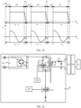
- Any charging cycle in the N charging cycles may include, as shown in FIG. 3b , a first phase P1, a second phase P2, and a third phase P3.
- the following describes a working process of the charging apparatus 02 in any charging cycle T in the N charging cycles.
- FIG. 3b shows, when the lower bridge switch Td is turned off, a waveform graph (an upper half part of FIG. 3b ) corresponding to a source-drain voltage (that is, a voltage Vds) corresponding to the lower bridge switch Td and a cycle T, and a waveform graph (a lower half part of FIG. 3b ) corresponding to a current of the clamp capacitor Cq and a cycle, where the waveform graph of Vds and the waveform graph of the current of clamp capacitor Cq are in an up-down correspondence.
- a waveform graph an upper half part of FIG. 3b
- a source-drain voltage that is, a voltage Vds
- the voltage Vds is not in the waveform graph corresponding to the voltage Vds and the cycle, and is represented by 0 herein.
- the current of the clamp capacitor Cq is also represented by 0 in the waveform graph corresponding to the current of the clamp capacitor Cq and the cycle.
- the lower bridge switch Td is turned off, and the upper bridge switch Tc is turned on.
- the primary coil Lm discharges electricity to the first secondary coil Ld through electromagnetic induction.
- a part of magnetic flux fails to be coupled to the first secondary coil Ld by using a magnetic core, and returns to the primary coil Lm through air closing, so that a leakage inductance Lr shown in FIG. 3c is generated in the primary coil Lm.
- the leakage inductance Lr in the primary coil Lm charges the clamp capacitor Cq to generate a forward current shown in FIG. 3b .
- the clamp capacitor Cq discharges electricity to the primary coil Lm to generate a negative current shown in FIG. 3b .
- the voltage value of the Vds remains unchanged.
- the leakage inductance Lr in the primary coil Lm charges and discharges electricity to the clamp capacitor Cq, and a voltage value corresponding to the leakage inductance Lr may be ignored because a capacity of the clamp capacitor Cq is relatively large. Therefore, the voltage value of Vds may always remain unchanged in the second phase P2.
- the lower bridge switch Td is turned off, and the upper bridge switch Tc is turned off, that is, this is dead time.
- a bottom-up current exists at a location of the primary coil Lm. Therefore, when the upper bridge switch Tc is turned off, under action of the current, power in a parasitic capacitor Cj2 in the lower bridge switch Td may be removed to generate a negative current. Therefore, in the third phase P3, there is a low negative current in the waveform graph corresponding to the current of the clamp capacitor Cq and the cycle.
- the power in the second parasitic capacitor Cj2 in the lower bridge switch Td is removed. Therefore, in this case, the voltage value of Vds rapidly drops to 0 or approaches 0.
- the charging apparatus 02 may include a plurality of charging cycles.
- a charging process in each charging cycle is the same as the foregoing, and details are not described herein again.
- the charging apparatus 02 provided in this embodiment of this application further includes a controller 203.
- the controller 203 may be electrically connected to a strobe end of the lower bridge switch Td and a strobe end of the upper bridge switch Tc by using the lower bridge drive circuit 205 and the upper bridge drive circuit 204.
- the strobe end is configured to control a switch to be turned on or turned off.
- the switch is a transistor
- the strobe end is a gate g of the transistor.
- the controller 203 outputs a logic signal in the first phase P1 and the second phase P2 of the charging cycle through an HIN port and LIN port to drive the upper bridge drive circuit 204 and the lower bridge drive circuit 205, so as to control the upper bridge switch Tc and the lower bridge switch Td to be alternatively turned on.
- a location at which the controller 203 is electrically connected to the transformer 202 may be referred to as a sampling point.
- the controller 203 may obtain, at the location of the sampling point, a voltage waveform at the location at which the controller 203 is electrically connected to the transformer 202, and use the voltage waveform as a sampling waveform.
- a sampling point A may be located between the second end (the lower end) of the primary coil Lm and the first end (the upper end) of the lower bridge switch Td, or between the second end (the lower end) of the upper bridge switch Tc and the first end (the upper end) of the lower bridge switch Td. It should be noted that FIG. 4a only shows an example location.
- the upper bridge switch Tc should be turned on but is not turned on, the leakage inductance Lr in the primary coil Lm can charge only the clamp capacitor Cq, and the clamp capacitor Cq cannot discharge electricity to the primary coil Lm by using the upper bridge switch Tc, which causes problems such as a short circuit or an open circuit that occurs when a voltage of the clamp capacitor Cq is excessively high.
- the controller 203 obtains the sampling waveform at the sampling point A through an SN port.
- a voltage of the sampling waveform at the sampling point A is equal to the sum of the output voltage Vo of the rectifier circuit 201 and the voltage Vb of the primary coil Lm.
- the output voltage Vo of the rectifier circuit 201 is a direct-current voltage, and therefore generates no impact on a change trend of the voltage waveform of the primary coil Lm.
- a sampling waveform obtained by the controller 203 at the sampling point A may include the voltage waveform of the primary coil Lm, so that the sampling waveform at the sampling point A and the voltage waveform of the primary coil Lm can change simultaneously with time.
- the controller 203 turns off the lower bridge switch Td in the first phase P1 of a next charging cycle, to prevent the leakage inductance Lr in the primary coil Lm from charging the clamp capacitor Cq, thereby avoiding problems such as a short circuit or an open circuit that occurs when a voltage of the clamp capacitor Cq is excessively high.
- next charging cycle refers to a charging cycle (for example, the (N + 1) th charging cycle) that is adjacent to a current charging cycle (for example, the N th charging cycle) in which it is determined whether the sampling waveform is abnormal and that appears after the N th charging cycle in a time sequence that is, a next charging cycle of the N th charging cycle.
- the parasitic capacitor Cj 1 included in the upper bridge switch Tc is connected in series to the clamp capacitor Cq.
- a capacitance value of an equivalent capacitor is less than a capacitance value of any of the first parasitic capacitor Cj 1 and the clamp capacitor Cq, and greatly decreases compared with a capacitance value (that is, the capacitance value of the clamp capacitor Cq) when the upper bridge switch Tc is turned on. Therefore, when the upper bridge switch Tc is not turned on, the leakage inductance Lr may quickly perform charging and discharging, thereby generating relatively high electromotive force.
- the sampling point is disposed between the second end (the lower end) of the primary coil Lm and the first end (the upper end) of the lower bridge switch Td.
- the waveform of the voltage Vb of the primary coil Lm is synchronous with the waveform of the voltage Vo 1 of the first secondary coil Ld, and a value of the output voltage Vo of the rectifier circuit 201 remains unchanged, so that as shown in FIG. 4b , the sampling point may be disposed on a side of an output voltage of the transformer 202, that is, the first end C (referred to as a sampling point C below) of the first secondary coil Ld.
- a sampling waveform obtained by the controller 203 at the sampling point C may include a voltage waveform of the first secondary coil Ld, so that the sampling waveform at the sampling point C and the voltage waveform of the first secondary coil Ld can change simultaneously with time.
- the controller 203 can control on/off of the upper bridge switch Tc and the lower bridge switch Td.
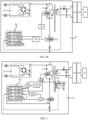
- the charging apparatus 02 provided in this embodiment of this application may further include a power supply circuit 501 shown in FIG. 5 .
- the power supply circuit 501 is electrically connected to the controller 203 through a VCC port.
- a GND port is disposed in the controller 203, and a voltage difference is formed between the VCC port and the GND port, so as to provide a voltage to the controller 203.
- the transformer 202 may further include a second secondary coil Lf and a second rectifier diode D2.
- a first end (an upper end) of the second secondary coil Lf is electrically connected to an anode of the second rectifier diode D2, and a cathode of the second rectifier diode D2 is electrically connected to the power supply circuit 501.
- a second electrode of the second secondary coil Lf is grounded.
- the second secondary coil Lf and the primary coil Lm are configured to buck the voltage Vb of the primary coil Lm through electromagnetic induction, and generate a second output voltage Vo2.
- the second output voltage Vo2 is used to supply power to the power supply circuit 501. After converting the voltage into a working voltage of the controller 203, the power supply circuit 501 transmits the voltage to the VCC port in the controller 203.
- the charging apparatus 02 further includes an upper bridge power supply unit 502 and a lower bridge power supply unit 503.
- the upper bridge power supply unit 502 is separately electrically connected to the power supply circuit 501 and the upper bridge drive circuit 204
- the lower bridge power supply unit 503 is separately electrically connected to the power supply circuit 501 and the lower bridge drive circuit 205.
- the upper bridge power supply unit 502 and the lower bridge power supply unit 503 are respectively converted into working voltages of the upper bridge drive circuit 204 and the lower bridge drive circuit 205 by using the power supply circuit 501, and then the working voltages are transmitted to the upper bridge power supply unit 502 and the lower bridge power supply unit 503.
- the controller 203 further includes a CS port, an O1 port, and an O2 port.
- the CS port is configured to monitor a current in a circuit when the lower bridge switch Td is turned on, so as to prevent an anomaly.
- the O1 port and the O2 port have other functions, which may be specifically set based on a situation.
- the sampling point may be located at the first end B (referred to as a sampling point B below) of the second secondary coil Lf shown in FIG. 5 .
- the second output voltage Vo2 of the second secondary coil Lf is simply obtained through electromagnetic induction of the primary coil Lm in the transformer 202, so that similarly, in same time, the voltage Vb of the primary coil Lm and the voltage Vo2 of the second secondary coil Lf are different only due to different quantities of turns of the coil. Therefore, the waveform of the voltage Vb of the primary coil Lm is synchronous with a waveform of the voltage Vo2 of the second secondary coil Lf, and a phase difference is 180°.
- a sampling waveform obtained by the controller 203 at the sampling point B may include the voltage waveform of the second secondary coil Lf, so that the sampling waveform at the sampling point B and the voltage waveform of the second secondary coil Lf can change simultaneously with time.
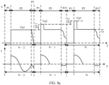
- the controller 203 determines, after obtaining a sampling waveform, that the waveform is abnormal is described below by using an example in which the sampling point is disposed between the second end (the lower end) of the primary coil Lm and the first end (the upper end) of the lower bridge switch Td.
- the sampling waveform in a current charging cycle is abnormal includes: In the second phase P2 of the N th charging cycle, the controller 203 obtains a peak voltage Vp of the sampling waveform, where the peak voltage Vp is greater than a voltage threshold Vth.
- the current charging cycle in this embodiment of this application is the N th charging cycle.
- an abnormal waveform refers to a corresponding waveform that has a shape different from that in FIG. 3b in the second phase P2.
- waveforms in the (N - 1) th cycle and the (N - 2) th cycle are normal waveforms, and a waveform in the N th cycle is an abnormal waveform.
- N is an integer greater than or equal to 3.
- the primary coil Lm discharges electricity to the first secondary coil Ld, and the voltage value of the first secondary coil Ld remains unchanged.
- the leakage inductance Lr in the primary coil Lm charges and discharges electricity to the clamp capacitor Cq
- the first parasitic capacitor Cj 1 is generated because the upper bridge switch Tc is not turned on.
- the leakage inductance Lr may quickly perform charging and discharging, thereby generating relatively high electromotive force. Therefore, in FIG. 6a , a voltage value of the abnormal waveform in the second phase P2 increases. However, when the leakage inductance Lr gradually decreases and ultimately becomes 0 due to a damping effect, the voltage is restored to a voltage the same as the normal waveform.
- the leakage inductance Lr in the primary coil Lm charges only the clamp capacitor Cq to generate a forward current. Because the upper bridge switch Tc is not turned on and the leakage inductance Lr cannot discharge electricity, a negative current cannot be generated. As a result, the voltage of the clamp capacitor Cq is excessively high, and problems such as a short circuit or an open circuit may occur.
- the voltage threshold Vth may be a platform voltage Vt.
- Vo is the output voltage of the rectifier circuit 201
- Vo 1 is the output voltage provided by the transformer 202 to the load 01, that is, the voltage of the first secondary coil Ld
- T1 is a ratio of a quantity of turns of the primary coil in the transformer to a quantity of turns of the secondary coil configured to supply power to the load (that is, a ratio of the quantity of turns of the primary coil Lm to a quantity of turns of the first secondary coil Ld)
- T2 is a ratio of the quantity of turns of the primary coil Lm to a quantity of turns of the second secondary coil Lf; and when the sampling point is the sampling point C shown in FIG. 4b , T2 is a ratio of the quantity of turns of the primary coil Lm to the quantity of turns of the first secondary coil Ld.
- the voltage threshold Vth may be a value near the platform voltage Vt, for example, the platform voltage ⁇ 20 V This is not limited in this application.
- the controller 203 may include a comparator.
- the comparator outputs a logic signal after comparing the peak voltage Vp with the voltage threshold Vth, to drive the lower bridge drive circuit 205 to perform an action.
- the controller 203 may calculate an integral area S (a part corresponding to a shadow part in the figure), in the second phase P2, that is of a part of the sampling waveform in the second phase P2 and that exceeds the voltage threshold Vth, where S > 0.
- the voltage threshold Vth may be the platform voltage Vt (that is, a manner shown in FIG. 6b ), or may be a value near the platform voltage Vt. This is not limited in this application.
- a setting manner is the same as that in the foregoing. Details are not described herein again.
- the controller 203 may include an integration unit and a comparison unit.
- the integration unit is configured to integrate an area
- the comparison unit is configured to output a logic signal after comparing an integrated area value with zero, to drive the lower bridge drive circuit 205 to perform.
- the charging apparatus 02 may further include a sampling circuit 701 shown in FIG. 7a .
- One end of the sampling circuit 701 may be electrically connected to the controller 203, and the other end of the sampling circuit 701 may be electrically connected to the lower end of the primary coil Lm in the transformer 202 by using the sampling point A.
- the sampling circuit 701 is configured to buck a voltage at a location at which the sampling circuit 701 is electrically connected to the transformer 202, that is, at the sampling point A, and then provide a bucked voltage to the controller 203. It should be noted that if the voltage value at the sampling point does not exceed a voltage withstand value of the controller 203, the sampling circuit 701 may not be disposed. This is not limited in this application.
- the sampling circuit 701 may include a first resistor R1 and a second resistor R2 that are shown in FIG. 7b .
- a first end (an upper end) of the first resistor R1 is electrically connected to the transformer 202
- a first end (an upper end) of the second resistor R2 is electrically connected to a second end (a lower end) of the first resistor R1 and the controller 203
- a second end (a lower end) of the second resistor R2 is grounded.
- a voltage value collected by the controller 203 may be changed by adjusting a ratio of a resistance value of the first resistor R1 to a resistance value of the second resistor R2, to ensure that the voltage value does not exceed the voltage withstand value of the controller.
- the ratio of the resistance value of the first resistor R1 to the resistance value of the second resistor R2 is larger, the collected voltage value is smaller.
- the sampling circuit 701 may include a first coil L1 and a second coil L2 that are shown in FIG. 7c .
- a first end (an upper end) of the first coil L1 is electrically connected to the transformer 202, and a second end (a lower end) of the first coil L1 is grounded.
- a first end M of the second coil L2 is electrically connected to the controller 203, and the other end of the second coil L2 is grounded.
- a quantity of turns of the first coil L1 is greater than a quantity of turns of the second coil L2.
- the voltage value collected by the controller 203 may be changed by controlling a ratio of the quantity of turns of the first coil L1 to the quantity of turns of the second coil L2.
- the ratio of the quantity of turns of the first coil L1 to the quantity of turns of the second coil L2 is larger, the collected voltage value is smaller.
- the sampling circuit 701 may include a third resistor R3 and a second capacitor C2 that are shown in FIG. 7d .
- a first end (an upper end) of the third resistor R3 is electrically connected to the controller 203, and a second end (a lower end) of the third resistor R3 is grounded.
- a first end (a right end) of the second capacitor C2 is electrically connected to the transformer 202, and a second end (a left end) of the second capacitor C2 is electrically connected to the controller 203.
- the voltage value collected by the controller 203 may be changed by adjusting a capacitance value of the second capacitor C2 or a resistance value of the third resistor R3. When the capacitance value of the second capacitor C2 or the resistance value of the third resistor R3 is larger, the collected voltage value is larger.
- sampling circuits 701. are merely several implementable examples of the sampling circuits 701. As long as the voltage bucking function can be implemented, another manner of disposing the sampling circuit 701 may also be adopted. This is not limited in this application.
- Example 2 whether the foregoing sampling waveform is abnormal means whether the sampling waveform in the second phase P2 of the N th cycle is abnormal, so as to determine whether the upper bridge switch Tc is turned on.
- a difference from Example 1 is that, in this example, that the sampling waveform in a current charging cycle is abnormal includes: The controller 203 continuously obtains a peak voltage Vp of the sampling waveform in the second phase P2 of each of the N th charging cycle shown in FIG.
- ⁇ V ⁇ 0 in the foregoing calculation result, it may indicate that the sampling waveform in the second phase P2 of the current charging cycle (that is, the N th charging cycle) is abnormal, and the upper bridge switch Tc is not turned on in the second phase P2 of the N th charging cycle.
- a value of N is the same as the foregoing.
- M M ⁇ 1, and M is a positive number.
- the waveform in the N th charging cycle is an abnormal waveform.
- the controller 203 is configured to output a logic signal after performing calculation on the peak voltage Vp, to drive the lower bridge drive circuit 205 to perform an action. It should be noted that a specific calculation manner is not limited in this application, provided that an abnormal waveform can be determined.
- the sampling waveform in a current charging cycle is abnormal includes: The controller 203 may continuously obtain an integral area S that is in the second phase and that is of a part exceeding the voltage threshold Vth in the second phase P2 of the N th charging cycle and in a second phase of each of M (as shown in the figure, M is 2) charging cycles before the N th charging cycle.
- the controller 203 calculates an area difference ⁇ S between integral areas S that are in two adjacent charging cycles and that are in the (M + 1) integral areas S ((M + 1) refers to the N th charging cycle and the M charging cycles before the N th charging cycle, as shown in FIG.
- the voltage threshold Vth may be the platform voltage Vt (this is used as an example in the figure), or may be a value near the platform voltage Vt. This is not limited in this application. A specific setting manner is the same as that in Example 1, and details are not described herein again.
- the controller 203 may include an integration unit and a processing unit.
- the integration unit is configured to integrate an area
- the processing unit is configured to output a logic signal after performing calculation on an integrated area value, to drive the lower bridge drive circuit 205 to perform an action.
- sampling circuit may also be disposed.
- a manner of disposing the sampling circuit is the same as that in the foregoing, and details are not described herein again.
- Example 1 whether the foregoing sampling waveform is abnormal means whether the sampling waveform in the second phase P2 of the N th cycle is abnormal, so as to determine whether the upper bridge switch Tc is turned on.
- a difference from Example 1 is that, in this example, as shown in FIG. 8c , that the sampling waveform in a current charging cycle is abnormal includes: The controller 203 obtains a platform voltage Vt of the sampling waveform in the second phase P2 of the (N - 1) th charging cycle and a peak voltage Vp of the sampling waveform in the second phase P2 of the N th charging cycle, where Vp > Vt. As shown in FIG.
- the controller 203 is configured to output a logic signal after obtaining and comparing the peak voltage Vp with the platform voltage Vt, to drive the lower bridge drive circuit 205 to perform an action.
- sampling circuit may also be disposed.
- a manner of disposing the sampling circuit is the same as that in the foregoing, and details are not described herein again.
- Example 1 whether the foregoing sampling waveform is abnormal means whether the sampling waveform in the second phase P2 of the N th cycle is abnormal, so as to determine whether the upper bridge switch Tc is turned on.
- a difference from Example 1 is that, in this example, as shown in FIG. 8d , that the sampling waveform in a current charging cycle is abnormal includes: The controller 203 learns that a voltage Vq of the sampling waveform is greater than or equal to the voltage threshold Vth (for example, 30 V) at an end of the third phase P3 of the N th charging cycle (that is, a start end of the first phase P1 of the (N + 1) th charging cycle). When the voltage Vq of the sampling waveform is greater than 30 V at the end of the third phase P3, loss is relatively large when the lower bridge switch Td is turned on.
- Vth for example, 30 V
- a voltage at the end of the third phase P3 of the N th charging cycle is Vq2
- a voltage at an end of the third phase P3 of in the (N -1) th charging cycle is Vq1.
- Vq2 > 30 V
- Vq1 0 V Therefore, a waveform corresponding to the current charging cycle, that is, the N th charging cycle, is an abnormal waveform, and a waveform corresponding to the (N - 1) th charging cycle is normal waveform.
- a value of N is the same as the foregoing.
- the voltage at the end of the third phase P3 of the N th charging cycle (that is, a start end of the first phase P1 of the (N + 1) th charging cycle) generates a negative current at a location of the primary coil Lm because the upper bridge switch Tc is turned on. Under action of the current, power in a parasitic capacitor in the lower bridge switch Td is removed, so that the voltage value of the sampling waveform rapidly drops to 0 or approaches 0.
- the upper bridge switch Tc is turned off, and the negative current does not exist, so that the voltage at the end of the third phase P3 of the N th charging cycle is relatively high.
- the voltage value at the end of the third phase P3 of the N th charging cycle may be detected to determine whether the sampling waveform in the current charging cycle is an abnormal waveform.
- the voltage threshold Vth is not limited in this application, and may be set based on a requirement.
- the controller 203 may include a comparator.
- the comparator outputs a logic signal after comparing the voltage Vq of the sampling waveform at the end of the third phase P3 with the voltage threshold Vth (for example, 30 V), to drive the lower bridge drive circuit 205 to perform an action.
- Vth for example, 30 V
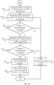
- a waveform determining method may include the following steps.
- the controller 203 obtains a waveform at a sampling point in the N th charging cycle, where N is an integer.
- Example 1 is a manner of comparing a peak voltage Vp or an integral area S of a waveform in a same cycle with a threshold.
- Example 2 is a manner of performing calculation on peak voltages Vp or integral areas S of waveforms in at least two consecutive cycles and then comparing a calculation result with a threshold.
- Example 3 is a manner of comparing a platform voltage Vt in a current cycle with a peak voltage Vp in a next cycle.
- Example 4 is a manner of comparing a voltage Vq at an end of the third phase P3 of a charging cycle with a threshold. For example, three manners that are respectively in Example 1, Example 2, and Example 3 may be selected for synchronous determining.
- N determining results are abnormal waveforms. (M is greater than or equal to N.) For example, the foregoing M manners are determined, and several of the M manners are checked, for example, N determining results all are abnormal waveforms.
- a final determining result is an abnormal waveform.
- the final determining result is an abnormal waveform. For example, if N is 3 and three determining results all are abnormal waveforms, the final determining result is an abnormal waveform.
- a final determining result is a normal waveform.
- a quantity of determining results that are abnormal waveforms is less than N (less than 3), the final determining result is a normal waveform.
- values ofM and N may be set based on a requirement. This is not limited in this application.
- a waveform determining method may include the following steps.
- the controller 203 obtains a waveform at a sampling point in the N th charging cycle, where N is an integer.
- Example 1 is a manner of comparing a peak voltage Vp or an integral area S of a waveform in a same cycle with a threshold.
- Example 2 is a manner of performing calculation on peak voltages Vp or integral areas S of waveforms in at least two consecutive cycles and then comparing a calculation result with a threshold.
- Example 3 is a manner of comparing a platform voltage Vt in a current cycle with a peak voltage Vp in a next cycle.
- Example 4 is a manner of comparing a voltage Vq at an end of the third phase P3 of a charging cycle with a threshold. For example, the manner in Example 1 may be selected for determining.
- S203 Check whether a determining result is an abnormal waveform. Specifically, the manner in S202 is determined to check whether the determining result is an abnormal waveform.
- step S205 Check whether a determining result is an abnormal waveform. Specifically, after step S204 is performed, it is checked whether the determining result is an abnormal waveform.
- a final determining result is a normal waveform. Specifically, if the determining results in S203 and S205 are normal waveforms, the final determining result is a normal waveform.
- a final determining result is an abnormal waveform. If the determining result in S205 is an abnormal waveform, the final determining result is an abnormal waveform.
Landscapes
- Engineering & Computer Science (AREA)
- Power Engineering (AREA)
- Manufacturing & Machinery (AREA)
- Chemical & Material Sciences (AREA)
- Chemical Kinetics & Catalysis (AREA)
- Electrochemistry (AREA)
- General Chemical & Material Sciences (AREA)
- Charge And Discharge Circuits For Batteries Or The Like (AREA)
- Dc-Dc Converters (AREA)
Claims (22)
- Ladegerät (02), das dazu konfiguriert ist, eine Last (01) mit Leistung zu versorgen, wobei das Ladegerät Folgendes umfasst:eine Gleichrichterschaltung (201), die dazu konfiguriert ist, einen empfangenen Wechselstrom gleichzurichten;einen Transformator (202), der dazu konfiguriert ist, eine Ausgangsspannung der Gleichrichterschaltung abzuschwächen und dann der Last eine abgeschwächte Ausgangsspannung bereitzustellen, wobei der Transformator eine Primärspule (Lm) und mindestens eine Sekundärspule (Ld) umfasst und ein erstes Ende der Primärspule elektrisch mit der Gleichrichterschaltung verbunden ist;einen unteren Brückenschalter (Td), wobei ein erstes Ende des unteren Brückenschalters elektrisch mit einem zweiten Ende der Primärspule verbunden ist, ein zweites Ende des unteren Brückenschalters geerdet ist und der untere Brückenschalter dazu konfiguriert ist, in einer ersten Phase eines Ladezyklus des Ladegeräts eingeschaltet zu werden, sodass ein von der Gleichrichterschaltung ausgegebener Strom an die Primärspule übertragen wird, um die Primärspule zu laden;einen Klemmkondensator (Cq), wobei ein erstes Ende des Klemmkondensators elektrisch mit dem ersten Ende der Primärspule verbunden ist;einen oberen Brückenschalter (Tc), wobei ein erstes Ende des oberen Brückenschalters elektrisch mit einem zweiten Ende des Klemmkondensators verbunden ist, ein zweites Ende des oberen Brückenschalters elektrisch mit dem zweiten Ende der Primärspule verbunden ist und der obere Brückenschalter dazu konfiguriert ist, in einer zweiten Phase des Ladezyklus eingeschaltet zu werden, sodass eine Streuinduktivität in der Primärspule den Klemmkondensator lädt und der Klemmkondensator Elektrizität an die Primärspule abgibt; undeine Steuerung (203), die dazu konfiguriert ist, in der ersten und der zweiten Phase den oberen Brückenschalter und den unteren Brückenschalter so zu steuern, dass sie abwechselnd eingeschaltet werden, wobei die Steuerung ferner zu Folgendem konfiguriert ist: wenn der untere Brückenschalter ausgeschaltet ist, Erlangen einer Abtastwellenform an einer Stelle, an der die Steuerung elektrisch mit dem Transformator verbunden ist; undwenn die Abtastwellenform in einem aktuellen Ladezyklus anormal ist, Ausschalten des unteren Brückenschalters in einer ersten Phase eines nächsten Ladezyklus, wobei die Abtastwellenform eine Spannungswellenform der Primärspule oder eine Spannungswellenform der Sekundärspule umfasst.
- Ladegerät nach Anspruch 1, wobei die Stelle, an der die Steuerung elektrisch mit dem Transformator verbunden ist, zwischen dem zweiten Ende der Primärspule und dem ersten Ende des unteren Brückenschalters oder zwischen dem zweiten Ende des oberen Brückenschalters und dem ersten Ende des unteren Brückenschalters liegt.
- Ladegerät nach Anspruch 1, wobei der Transformator eine erste Sekundärspule (Ld) umfasst und der Transformator ferner eine erste Gleichrichterdiode (D1) umfasst; ein erstes Ende der ersten Sekundärspule elektrisch mit einer Anode der ersten Gleichrichterdiode verbunden ist, eine Kathode der ersten Gleichrichterdiode dazu konfiguriert ist, elektrisch mit der Last verbunden zu sein, und ein zweites Ende der ersten Sekundärspule geerdet ist; und die erste Sekundärspule und die Primärspule dazu konfiguriert sind, eine Spannung der Primärspule durch elektromagnetische Induktion abzuschwächen und eine erste Ausgangsspannung zu erzeugen; und
die Stelle, an der die Steuerung elektrisch mit dem Transformator verbunden ist, an dem ersten Ende der ersten Sekundärspule liegt. - Ladegerät nach Anspruch 3, wobei das Ladegerät ferner eine Leistungsversorgungsschaltung (501) umfasst und die Leistungsversorgungsschaltung elektrisch mit der Steuerung verbunden und dazu konfiguriert ist, die Steuerung mit Leistung zu versorgen;der Transformator ferner eine zweite Sekundärspule (Lf) und eine zweite Gleichrichterdiode (D2) umfasst;ein erstes Ende der zweiten Sekundärspule elektrisch mit einer Anode der zweiten Gleichrichterdiode verbunden ist, eine Kathode der zweiten Gleichrichterdiode elektrisch mit der Leistungsversorgungsschaltung verbunden ist und eine zweite Elektrode der zweiten Sekundärspule geerdet ist; die zweite Sekundärspule und die Primärspule dazu konfiguriert sind, die Spannung der Primärspule durch elektromagnetische Induktion abzuschwächen und eine zweite Ausgangsspannung zu erzeugen, wobei die zweite Ausgangsspannung verwendet wird, um die Leistungsversorgungsschaltung mit Leistung zu versorgen; unddie Stelle, an der die Steuerung elektrisch mit dem Transformator verbunden ist, an dem ersten Ende der zweiten Sekundärspule liegt.
- Ladegerät nach einem der Ansprüche 1 bis 4, das derart konfiguriert ist, dass
Bestimmen, dass die Abtastwellenform in einem aktuellen Ladezyklus anormal ist, Folgendes umfasst:Erlangen, durch die Steuerung, einer Plattformspannung Vt der Abtastwellenform in einer zweiten Phase eines N-ten Ladezyklus und Erkennen in der zweiten Phase, dass eine Spitzenspannung Vp der Abtastwellenform größer als die Plattformspannung Vt ist;oder Berechnen in der zweiten Phase einer Integralfläche S in der zweiten Phase, die aus einem Teil der Abtastwellenform besteht und die Plattformspannung Vt übersteigt, wobei S > 0, N ≥ 1 und N eine positive Zahl ist. - Ladegerät nach einem der Ansprüche 1 bis 4, das derart konfiguriert ist, dass
Bestimmen, dass die Abtastwellenform in einem aktuellen Ladezyklus anormal ist, Folgendes umfasst:Erlangen, durch die Steuerung, einer Plattformspannung Vt der Abtastwellenform in einer zweiten Phase eines N-ten Ladezyklus;kontinuierliches Erlangen einer Integralfläche S, die in der zweiten Phase ist und die aus einem Teil besteht, der die Plattformspannung Vt übersteigt, in der zweiten Phase des N-ten Ladezyklus und in einer zweiten Phase jedes von M Ladezyklen vor dem N-ten Ladezyklus; und Berechnen einer Flächendifferenz ΔS zwischen Integralflächen S, die in zwei benachbarten Ladezyklen sind und die in den (M + 1) Integralflächen S sind, wobei ΔS ≠ 0, N ≥ 1, N eine positive Zahl ist, M ≥ 1 und M eine positive Zahl ist. - Ladegerät nach einem der Ansprüche 1 bis 4, das derart konfiguriert ist, dass
Bestimmen, dass die Abtastwellenform in einem aktuellen Ladezyklus anormal ist, Folgendes umfasst:
Erlangen, durch die Steuerung, einer Plattformspannung Vt der Abtastwellenform in einer zweiten Phase eines (N-1)-ten Ladezyklus; und Erlangen einer Spitzenspannung Vp der Abtastwellenform in einer zweiten Phase eines N-ten Ladezyklus, wobei Vp > Vt, N ≥ 2 und N eine positive Zahl ist. - Ladegerät nach einem der Ansprüche 5 bis 7, wobei, wenn die Steuerung elektrisch mit der Primärspule verbunden ist, die Plattformspannung Vt = (Vo + Vo1 × T1) beträgt, wobei Vo die Ausgangsspannung der Gleichrichterschaltung ist, Vo1 die der Last von dem Transformator bereitgestellte Ausgangsspannung ist und T1 ein Verhältnis einer Anzahl von Windungen der Primärspule in dem Transformator zu einer Anzahl von Windungen einer Sekundärspule ist, die dazu konfiguriert ist, die Last mit Leistung zu versorgen; oder
wenn die Steuerung elektrisch mit der Sekundärspule verbunden ist, die Plattformspannung Vt = -Vo/T2 beträgt, wobei T2 ein Verhältnis einer Anzahl von Windungen der Primärspule in dem Transformator zu einer Anzahl von Windungen der Sekundärspule ist, die elektrisch mit der Steuerung verbunden ist. - Ladegerät nach einem der Ansprüche 1 bis 4, das derart konfiguriert ist, dass
Bestimmen, dass die Abtastwellenform in einem aktuellen Ladezyklus anormal ist, Folgendes umfasst:
kontinuierliches Erlangen, durch die Steuerung, einer Spitzenspannung Vp der Abtastwellenform in einer zweiten Phase eines N-ten Ladezyklus und in einer zweiten Phase jedes von M Ladezyklen vor dem N-ten Ladezyklus; und Berechnen einer Spannungsdifferenz ΔV zwischen Spitzenspannungen Vp der Abtastwellenform, die in zwei benachbarten Ladezyklen vorliegen und die in den (M + 1) Spitzenspannungen Vp sind, wobei ΔV ≠ 0, N ≥ 1, N eine positive Zahl, M ≥ 1 und M eine positive Zahl ist. - Ladegerät nach einem der Ansprüche 1 bis 4, das derart konfiguriert ist, dass
Bestimmen, dass die Abtastwellenform in einem aktuellen Ladezyklus anormal ist, Folgendes umfasst:
Lernen, durch die Steuerung, dass eine Spannung der Abtastwellenform an einem Ende einer dritten Phase eines N-ten Ladezyklus größer oder gleich 30 V ist, wobei N ≥ 1 und N eine positive Zahl ist. - Ladegerät nach Anspruch 1, wobei das Ladegerät ferner Folgendes umfasst:
eine Abtastschaltung, die elektrisch zwischen der Steuerung und dem Transformator verbunden ist, wobei die Abtastschaltung dazu konfiguriert ist, eine Spannung an einer Stelle abzuschwächen, an der die Abtastschaltung elektrisch mit dem Transformator verbunden ist, und dann der Steuerung eine abgeschwächte Spannung bereitzustellen. - Ladegerät nach Anspruch 11, wobei die Abtastschaltung Folgendes umfasst:einen ersten Widerstand (R1), wobei ein erstes Ende des ersten Widerstands elektrisch mit dem Transformator verbunden ist; undeinen zweiten Widerstand (R2), wobei ein erstes Ende des zweiten Widerstands elektrisch mit einem zweiten Ende des ersten Widerstands und der Steuerung verbunden ist und ein zweites Ende des zweiten Widerstands geerdet ist.
- Ladegerät nach Anspruch 11, wobei die Abtastschaltung Folgendes umfasst:eine erste Spule (L1), wobei ein erstes Ende der ersten Spule elektrisch mit dem Transformator verbunden ist und ein zweites Ende der ersten Spule geerdet ist;eine zweite Spule (L2), wobei ein erstes Ende der zweiten Spule elektrisch mit der Steuerung verbunden ist und das andere Ende der zweiten Spule geerdet ist; undeine Anzahl von Windungen der ersten Spule größer als eine Anzahl von Windungen der zweiten Spule ist.
- Ladegerät nach Anspruch 11, wobei die Abtastschaltung Folgendes umfasst:einen dritten Widerstand (R3), wobei ein erstes Ende des dritten Widerstands elektrisch mit der Steuerung verbunden ist und ein zweites Ende des dritten Widerstands geerdet ist; undeinen zweiten Kondensator (C2), wobei ein erstes Ende des zweiten Kondensators elektrisch mit dem Transformator verbunden ist und ein zweites Ende des zweiten Kondensators elektrisch mit der Steuerung verbunden ist.
- Ladesystem, das eine elektronische Vorrichtung und das Ladegerät nach einem der Ansprüche 1 bis 14 umfasst, wobei die elektronische Vorrichtung eine Batterie umfasst und die Batterie elektrisch mit dem Ladegerät verbunden ist.
- Steuerverfahren für ein Ladegerät, wobei das Steuerverfahren für ein Ladegerät auf ein Ladegerät angewendet wird und das Ladegerät eine Gleichrichterschaltung, einen Transformator, einen unteren Brückenschalter, einen Klemmkondensator, einen oberen Brückenschalter und eine Steuerung umfasst; der Transformator eine Primärspule und mindestens eine Sekundärspule umfasst; ein erstes Ende der Primärspule elektrisch mit der Gleichrichterschaltung verbunden ist; die Steuerung elektrisch mit dem Transformator verbunden ist; ein erstes Ende des unteren Brückenschalters elektrisch mit einem zweiten Ende der Primärspule verbunden ist und ein zweites Ende des unteren Brückenschalters elektrisch mit einem Erdungsende verbunden ist;ein erstes Ende des Klemmkondensators elektrisch mit dem ersten Ende der Primärspule verbunden ist; und ein erstes Ende des oberen Brückenschalters elektrisch mit einem zweiten Ende des Klemmkondensators verbunden ist und ein zweites Ende des oberen Brückenschalters elektrisch mit dem zweiten Ende der Primärspule verbunden ist, wobeidas Steuerverfahren für ein Ladegerät Folgendes umfasst:Steuern, durch die Steuerung in einer ersten Phase eines Ladezyklus des Ladegeräts, des unteren Brückenschalters, um eingeschaltet zu werden, und des oberen Brückenschalters, um ausgeschaltet zu werden, sodass ein von der Gleichrichterschaltung ausgegebener Strom die Primärspule auflädt; undSteuern, durch die Steuerung in einer zweiten Phase des Ladezyklus, des unteren Brückenschalters, um ausgeschaltet zu werden, und des oberen Brückenschalters, um eingeschaltet zu werden, sodass die Primärspule Elektrizität abgibt, der Transformator eine Ausgangsspannung der Gleichrichterschaltung abschwächt und einer Last eine abgeschwächte Spannung bereitstellt, eine Streuinduktivität in der Primärspule den Klemmkondensator lädt und wenn die Streuinduktivität keinen Strom zum Ausgeben aufweist, der Klemmkondensator Elektrizität an die Primärspule abgibt; unddas Steuerverfahren für ein Ladegerät ferner einen Wellenformverarbeitungsschritt umfasst: Erlangen, durch die Steuerung in der zweiten Phase des Ladezyklus, einer Abtastwellenform an einer Stelle, an der die Steuerung elektrisch mit dem Transformator verbunden ist, wobei die Abtastwellenform eine Spannungswellenform der Primärspule oder eine Spannungswellenform der Sekundärspule umfasst; undwenn die Abtastwellenform in einem aktuellen Ladezyklus anormal ist, Ausschalten, durch die Steuerung, des unteren Brückenschalters in einer ersten Phase eines nächsten Ladezyklus.
- Steuerverfahren für ein Ladegerät nach Anspruch 16, wobei dass die Abtastwellenform in einem aktuellen Ladezyklus anormal ist, Folgendes umfasst:Erlangen, durch die Steuerung, einer Plattformspannung Vt der Abtastwellenform in einer zweiten Phase des N-ten Ladezyklus und Erkennen in der zweiten Phase, dass eine Spitzenspannung Vp der Abtastwellenform größer als die Plattformspannung Vt ist; oderBerechnen in der zweiten Phase einer Integralfläche S in der zweiten Phase, die aus einem Teil der Abtastwellenform besteht und die Plattformspannung Vt übersteigt, wobei S > 0, N ≥ 1 und N eine positive Zahl ist.
- Steuerverfahren für ein Ladegerät nach Anspruch 16, wobei dass die Abtastwellenform in einem aktuellen Ladezyklus anormal ist, Folgendes umfasst:Erlangen, durch die Steuerung, einer Plattformspannung Vt der Abtastwellenform in einer zweiten Phase eines N-ten Ladezyklus;kontinuierliches Erlangen einer Integralfläche S, die in der zweiten Phase ist und die aus einem Teil besteht, der die Plattformspannung Vt übersteigt, in der zweiten Phase des N-ten Ladezyklus und in einer zweiten Phase jedes von M Ladezyklen vor dem N-ten Ladezyklus; und Berechnen einer Flächendifferenz ΔS zwischen Integralflächen S, die in zwei benachbarten Ladezyklen sind und die in den (M + 1) Integralflächen S sind, wobei ΔS ≠ 0, N ≥ 1, N eine positive Zahl ist, M ≥ 1 und M eine positive Zahl ist.
- Steuerverfahren für ein Ladegerät nach Anspruch 16, wobei dass die Abtastwellenform in einem aktuellen Ladezyklus anormal ist, Folgendes umfasst:
Erlangen, durch die Steuerung, einer Plattformspannung Vt der Abtastwellenform in einer zweiten Phase des (N-1)-ten Ladezyklus; und Erlangen einer Spitzenspannung Vp der Abtastwellenform in einer zweiten Phase des N-ten Ladezyklus, wobei Vp > Vt, N ≥ 2 und N eine positive Zahl ist. - Steuerverfahren für ein Ladegerät nach einem der Ansprüche 17 bis 19, wobei, wenn die Steuerung elektrisch mit der Primärspule verbunden ist, die Plattformspannung Vt = (Vo + Vo1 × T1) beträgt, wobei Vo die Ausgangsspannung der Gleichrichterschaltung ist, Vo1 die der Last von dem Transformator bereitgestellte Ausgangsspannung ist und T1 ein Verhältnis einer Anzahl von Windungen der Primärspule in dem Transformator zu einer Anzahl von Windungen einer Sekundärspule ist, die dazu konfiguriert ist, die Last mit Leistung zu versorgen; oder
wenn die Steuerung elektrisch mit der Sekundärspule verbunden ist, die Plattformspannung Vt = -Vo/T2 beträgt, wobei T2 ein Verhältnis einer Anzahl von Windungen der Primärspule in dem Transformator zu einer Anzahl von Windungen der Sekundärspule ist, die elektrisch mit der Steuerung verbunden ist. - Steuerverfahren für ein Ladegerät nach Anspruch 16, wobei dass die Abtastwellenform in einem aktuellen Ladezyklus anormal ist, Folgendes umfasst:
kontinuierliches Erlangen, durch die Steuerung, einer Spitzenspannung Vp der Abtastwellenform in einer zweiten Phase eines N-ten Ladezyklus und in einer zweiten Phase jedes von M Ladezyklen vor dem N-ten Ladezyklus; und Berechnen einer Spannungsdifferenz ΔV zwischen Spitzenspannungen Vp der Abtastwellenform, die in zwei benachbarten Ladezyklen vorliegen und die in den (M + 1) Spitzenspannungen Vp sind, wobei ΔV ≠ 0, N ≥ 1, N eine positive Zahl, M ≥ 1 und M eine positive Zahl ist. - Steuerverfahren für ein Ladegerät nach Anspruch 16, wobei dass die Abtastwellenform in einem aktuellen Ladezyklus anormal ist, Folgendes umfasst:
Lernen, durch die Steuerung, dass eine Spannung der Abtastwellenform an einem Ende einer dritten Phase des N-ten Ladezyklus größer oder gleich 30 V ist, wobei N ≥ 1 und N eine positive Zahl ist.
Applications Claiming Priority (2)
| Application Number | Priority Date | Filing Date | Title |
|---|---|---|---|
| CN202010279469.9A CN111525662B (zh) | 2020-04-10 | 2020-04-10 | 一种充电装置及其控制方法、充电系统 |
| PCT/CN2021/078780 WO2021203870A1 (zh) | 2020-04-10 | 2021-03-02 | 一种充电装置及其控制方法、充电系统 |
Publications (3)
| Publication Number | Publication Date |
|---|---|
| EP4102677A1 EP4102677A1 (de) | 2022-12-14 |
| EP4102677A4 EP4102677A4 (de) | 2023-07-26 |
| EP4102677B1 true EP4102677B1 (de) | 2024-08-21 |
Family
ID=71902739
Family Applications (1)
| Application Number | Title | Priority Date | Filing Date |
|---|---|---|---|
| EP21785177.3A Active EP4102677B1 (de) | 2020-04-10 | 2021-03-02 | Ladegerät, steuerverfahren dafür und ladesystem |
Country Status (4)
| Country | Link |
|---|---|
| US (1) | US12580389B2 (de) |
| EP (1) | EP4102677B1 (de) |
| CN (2) | CN114844185B (de) |
| WO (1) | WO2021203870A1 (de) |
Families Citing this family (1)
| Publication number | Priority date | Publication date | Assignee | Title |
|---|---|---|---|---|
| CN114844185B (zh) | 2020-04-10 | 2024-09-24 | 华为数字能源技术有限公司 | 一种充电装置及其控制方法、充电系统 |
Family Cites Families (22)
| Publication number | Priority date | Publication date | Assignee | Title |
|---|---|---|---|---|
| CN1059988C (zh) * | 1998-08-20 | 2000-12-27 | 深圳市华为电气股份有限公司 | 高效率多路输出电源 |
| JP2002153054A (ja) * | 2000-11-10 | 2002-05-24 | Fujitsu Ltd | スイッチング電源回路 |
| US6947297B2 (en) * | 2003-10-04 | 2005-09-20 | Delta Electronics, Inc. | Active resonant snubber for DC-DC converter |
| CN102122890B (zh) * | 2010-10-11 | 2014-01-22 | 南京航空航天大学 | 一种有源钳位反激变换器辅助开关管的控制方法 |
| CN102307017B (zh) * | 2011-09-16 | 2014-09-10 | 浙江大学 | 一种应用于有源箝位反激式微型光伏并网逆变器装置的控制方法 |
| CN104505927A (zh) * | 2014-12-18 | 2015-04-08 | 广东易事特电源股份有限公司 | 反激式充电电路、反激式充电电路的控制方法及装置 |
| DE102014119531B4 (de) | 2014-12-23 | 2019-06-27 | Infineon Technologies Ag | Sensorschaltung |
| CN205213096U (zh) * | 2015-10-27 | 2016-05-04 | 浙江生辉照明有限公司 | Led智能控制电路及led照明装置 |
| US10069426B2 (en) * | 2016-03-12 | 2018-09-04 | Semiconductor Components Industries, Llc | Active clamp flyback converter |
| CN205911955U (zh) * | 2016-07-19 | 2017-01-25 | 深圳南云微电子有限公司 | 有源钳位的反激电路 |
| US10148188B2 (en) * | 2016-09-06 | 2018-12-04 | Fairchild Semiconductor Corporation | Clamp voltage detection and over-voltage protection for power supply topologies |
| US10148181B2 (en) * | 2016-10-07 | 2018-12-04 | Semiconductor Components Industries, Llc | Switched mode power supply with dynamic frequency foldback |
| US10651749B2 (en) * | 2016-11-07 | 2020-05-12 | Delta Electronics, Inc. | Flyback converter with a passive clamp |
| US10491097B2 (en) * | 2017-04-03 | 2019-11-26 | Texas Instruments Incorporated | Switching time optimizer for soft switching of an isolated converter |
| CN109067181B (zh) * | 2018-07-18 | 2019-11-22 | 东南大学 | 有源钳位反激变换器的自适应同步整流控制系统及控制方法 |
| CN108988652A (zh) * | 2018-09-10 | 2018-12-11 | 杰华特微电子(张家港)有限公司 | 反激有源钳位电路及其控制方法 |
| CN109245569B (zh) * | 2018-09-18 | 2020-04-24 | 西安矽力杰半导体技术有限公司 | 反激式变换器及其控制电路 |
| CN109639149B (zh) * | 2018-12-26 | 2020-07-28 | 西安华为技术有限公司 | 一种acf变换器、电压变换方法及电子设备 |
| CN210120487U (zh) * | 2019-04-30 | 2020-02-28 | 茂硕电源科技股份有限公司 | 钳位电路和反激变换器 |
| CN110829557B (zh) * | 2019-11-04 | 2025-01-14 | 国网江苏省电力有限公司江阴市供电分公司 | 一种隔离型无电解电容恒流充电电路及其切换方法 |
| CN110794279B (zh) * | 2019-11-15 | 2024-08-23 | 杰华特微电子股份有限公司 | 钳位开关管异常检测方法、检测电路及开关电路 |
| CN114844185B (zh) * | 2020-04-10 | 2024-09-24 | 华为数字能源技术有限公司 | 一种充电装置及其控制方法、充电系统 |
-
2020
- 2020-04-10 CN CN202210288033.5A patent/CN114844185B/zh active Active
- 2020-04-10 CN CN202010279469.9A patent/CN111525662B/zh active Active
-
2021
- 2021-03-02 EP EP21785177.3A patent/EP4102677B1/de active Active
- 2021-03-02 WO PCT/CN2021/078780 patent/WO2021203870A1/zh not_active Ceased
-
2022
- 2022-09-28 US US17/955,290 patent/US12580389B2/en active Active
Also Published As
| Publication number | Publication date |
|---|---|
| US20230013471A1 (en) | 2023-01-19 |
| EP4102677A4 (de) | 2023-07-26 |
| CN111525662B (zh) | 2022-03-29 |
| CN114844185B (zh) | 2024-09-24 |
| WO2021203870A1 (zh) | 2021-10-14 |
| CN111525662A (zh) | 2020-08-11 |
| CN114844185A (zh) | 2022-08-02 |
| EP4102677A1 (de) | 2022-12-14 |
| US12580389B2 (en) | 2026-03-17 |
Similar Documents
| Publication | Publication Date | Title |
|---|---|---|
| US8953347B2 (en) | Capacitor discharging circuit and power converter | |
| JP4500481B2 (ja) | スイッチング電源 | |
| US9124184B2 (en) | DC/DC converter | |
| US7577003B2 (en) | Switching power supply | |
| US7852051B2 (en) | Current-limiting circuit and method for operating the circuit | |
| KR20010075362A (ko) | 과전력 및 과전류 보호를 위한 공진 모드 전원 | |
| CN114337235B (zh) | 防浪涌雷击的电源及电源控制方法 | |
| US20110292693A1 (en) | Direct-current power supply device | |
| EP3439135B1 (de) | Vorrichtung zum drahtlosen stromempfang | |
| US20110194316A1 (en) | Switching power supply device | |
| KR102182886B1 (ko) | 컨버터의 데드타임 가변 시스템 및 데드타임 가변 방법 | |
| JP2010124572A (ja) | スイッチング電源装置 | |
| CN211656009U (zh) | 开关电源的控制装置、芯片及开关电源 | |
| US10811868B2 (en) | Electrical system and method for protecting a DC/DC converter | |
| CN1578052B (zh) | Ac适配器及其充电方法 | |
| WO2010125751A1 (ja) | スイッチング電源装置 | |
| EP4102677B1 (de) | Ladegerät, steuerverfahren dafür und ladesystem | |
| KR102143254B1 (ko) | 플라이백 컨버터의 pwm 제어장치 | |
| US6487092B2 (en) | DC/DC converter | |
| US20190386574A1 (en) | Power supply and power supply unit | |
| US20060164776A1 (en) | Current-limiting circuit and method for operating the circuit | |
| CN113659823B (zh) | 有源钳位反激电路的死区时间的确定方法 | |
| JP2010252610A (ja) | Dc−dcコンバータ | |
| CN113726175A (zh) | 转换装置、控制器及其供电控制方法 | |
| CN216290693U (zh) | 转换装置及控制器 |
Legal Events
| Date | Code | Title | Description |
|---|---|---|---|
| STAA | Information on the status of an ep patent application or granted ep patent |
Free format text: STATUS: THE INTERNATIONAL PUBLICATION HAS BEEN MADE |
|
| PUAI | Public reference made under article 153(3) epc to a published international application that has entered the european phase |
Free format text: ORIGINAL CODE: 0009012 |
|
| STAA | Information on the status of an ep patent application or granted ep patent |
Free format text: STATUS: REQUEST FOR EXAMINATION WAS MADE |
|
| 17P | Request for examination filed |
Effective date: 20220905 |
|
| AK | Designated contracting states |
Kind code of ref document: A1 Designated state(s): AL AT BE BG CH CY CZ DE DK EE ES FI FR GB GR HR HU IE IS IT LI LT LU LV MC MK MT NL NO PL PT RO RS SE SI SK SM TR |
|
| DAV | Request for validation of the european patent (deleted) | ||
| DAX | Request for extension of the european patent (deleted) | ||
| A4 | Supplementary search report drawn up and despatched |
Effective date: 20230627 |
|
| RIC1 | Information provided on ipc code assigned before grant |
Ipc: H02M 3/335 20060101ALI20230621BHEP Ipc: H02M 1/34 20070101ALI20230621BHEP Ipc: H02J 7/00 20060101AFI20230621BHEP |
|
| GRAP | Despatch of communication of intention to grant a patent |
Free format text: ORIGINAL CODE: EPIDOSNIGR1 |
|
| STAA | Information on the status of an ep patent application or granted ep patent |
Free format text: STATUS: GRANT OF PATENT IS INTENDED |
|
| INTG | Intention to grant announced |
Effective date: 20240417 |
|
| GRAS | Grant fee paid |
Free format text: ORIGINAL CODE: EPIDOSNIGR3 |
|
| GRAA | (expected) grant |
Free format text: ORIGINAL CODE: 0009210 |
|
| STAA | Information on the status of an ep patent application or granted ep patent |
Free format text: STATUS: THE PATENT HAS BEEN GRANTED |
|
| P01 | Opt-out of the competence of the unified patent court (upc) registered |
Free format text: CASE NUMBER: APP_36963/2024 Effective date: 20240620 |
|
| AK | Designated contracting states |
Kind code of ref document: B1 Designated state(s): AL AT BE BG CH CY CZ DE DK EE ES FI FR GB GR HR HU IE IS IT LI LT LU LV MC MK MT NL NO PL PT RO RS SE SI SK SM TR |
|
| REG | Reference to a national code |
Ref country code: GB Ref legal event code: FG4D |
|
| REG | Reference to a national code |
Ref country code: CH Ref legal event code: EP |
|
| REG | Reference to a national code |
Ref country code: IE Ref legal event code: FG4D |
|
| REG | Reference to a national code |
Ref country code: DE Ref legal event code: R096 Ref document number: 602021017638 Country of ref document: DE |
|
| REG | Reference to a national code |
Ref country code: LT Ref legal event code: MG9D |
|
| REG | Reference to a national code |
Ref country code: NL Ref legal event code: MP Effective date: 20240821 |
|
| PG25 | Lapsed in a contracting state [announced via postgrant information from national office to epo] |
Ref country code: NO Free format text: LAPSE BECAUSE OF FAILURE TO SUBMIT A TRANSLATION OF THE DESCRIPTION OR TO PAY THE FEE WITHIN THE PRESCRIBED TIME-LIMIT Effective date: 20241121 |
|
| REG | Reference to a national code |
Ref country code: AT Ref legal event code: MK05 Ref document number: 1716488 Country of ref document: AT Kind code of ref document: T Effective date: 20240821 |
|
| PG25 | Lapsed in a contracting state [announced via postgrant information from national office to epo] |
Ref country code: PT Free format text: LAPSE BECAUSE OF FAILURE TO SUBMIT A TRANSLATION OF THE DESCRIPTION OR TO PAY THE FEE WITHIN THE PRESCRIBED TIME-LIMIT Effective date: 20241223 Ref country code: NL Free format text: LAPSE BECAUSE OF FAILURE TO SUBMIT A TRANSLATION OF THE DESCRIPTION OR TO PAY THE FEE WITHIN THE PRESCRIBED TIME-LIMIT Effective date: 20240821 Ref country code: GR Free format text: LAPSE BECAUSE OF FAILURE TO SUBMIT A TRANSLATION OF THE DESCRIPTION OR TO PAY THE FEE WITHIN THE PRESCRIBED TIME-LIMIT Effective date: 20241122 Ref country code: PL Free format text: LAPSE BECAUSE OF FAILURE TO SUBMIT A TRANSLATION OF THE DESCRIPTION OR TO PAY THE FEE WITHIN THE PRESCRIBED TIME-LIMIT Effective date: 20240821 Ref country code: FI Free format text: LAPSE BECAUSE OF FAILURE TO SUBMIT A TRANSLATION OF THE DESCRIPTION OR TO PAY THE FEE WITHIN THE PRESCRIBED TIME-LIMIT Effective date: 20240821 |
|
| PG25 | Lapsed in a contracting state [announced via postgrant information from national office to epo] |
Ref country code: BG Free format text: LAPSE BECAUSE OF FAILURE TO SUBMIT A TRANSLATION OF THE DESCRIPTION OR TO PAY THE FEE WITHIN THE PRESCRIBED TIME-LIMIT Effective date: 20240821 |
|
| PG25 | Lapsed in a contracting state [announced via postgrant information from national office to epo] |
Ref country code: LV Free format text: LAPSE BECAUSE OF FAILURE TO SUBMIT A TRANSLATION OF THE DESCRIPTION OR TO PAY THE FEE WITHIN THE PRESCRIBED TIME-LIMIT Effective date: 20240821 |
|
| PG25 | Lapsed in a contracting state [announced via postgrant information from national office to epo] |
Ref country code: AT Free format text: LAPSE BECAUSE OF FAILURE TO SUBMIT A TRANSLATION OF THE DESCRIPTION OR TO PAY THE FEE WITHIN THE PRESCRIBED TIME-LIMIT Effective date: 20240821 Ref country code: IS Free format text: LAPSE BECAUSE OF FAILURE TO SUBMIT A TRANSLATION OF THE DESCRIPTION OR TO PAY THE FEE WITHIN THE PRESCRIBED TIME-LIMIT Effective date: 20241221 |
|
| PG25 | Lapsed in a contracting state [announced via postgrant information from national office to epo] |
Ref country code: HR Free format text: LAPSE BECAUSE OF FAILURE TO SUBMIT A TRANSLATION OF THE DESCRIPTION OR TO PAY THE FEE WITHIN THE PRESCRIBED TIME-LIMIT Effective date: 20240821 |
|
| PG25 | Lapsed in a contracting state [announced via postgrant information from national office to epo] |
Ref country code: ES Free format text: LAPSE BECAUSE OF FAILURE TO SUBMIT A TRANSLATION OF THE DESCRIPTION OR TO PAY THE FEE WITHIN THE PRESCRIBED TIME-LIMIT Effective date: 20240821 Ref country code: RS Free format text: LAPSE BECAUSE OF FAILURE TO SUBMIT A TRANSLATION OF THE DESCRIPTION OR TO PAY THE FEE WITHIN THE PRESCRIBED TIME-LIMIT Effective date: 20241121 |
|
| PG25 | Lapsed in a contracting state [announced via postgrant information from national office to epo] |
Ref country code: RS Free format text: LAPSE BECAUSE OF FAILURE TO SUBMIT A TRANSLATION OF THE DESCRIPTION OR TO PAY THE FEE WITHIN THE PRESCRIBED TIME-LIMIT Effective date: 20241121 Ref country code: PT Free format text: LAPSE BECAUSE OF FAILURE TO SUBMIT A TRANSLATION OF THE DESCRIPTION OR TO PAY THE FEE WITHIN THE PRESCRIBED TIME-LIMIT Effective date: 20241223 Ref country code: PL Free format text: LAPSE BECAUSE OF FAILURE TO SUBMIT A TRANSLATION OF THE DESCRIPTION OR TO PAY THE FEE WITHIN THE PRESCRIBED TIME-LIMIT Effective date: 20240821 Ref country code: NO Free format text: LAPSE BECAUSE OF FAILURE TO SUBMIT A TRANSLATION OF THE DESCRIPTION OR TO PAY THE FEE WITHIN THE PRESCRIBED TIME-LIMIT Effective date: 20241121 Ref country code: NL Free format text: LAPSE BECAUSE OF FAILURE TO SUBMIT A TRANSLATION OF THE DESCRIPTION OR TO PAY THE FEE WITHIN THE PRESCRIBED TIME-LIMIT Effective date: 20240821 Ref country code: LV Free format text: LAPSE BECAUSE OF FAILURE TO SUBMIT A TRANSLATION OF THE DESCRIPTION OR TO PAY THE FEE WITHIN THE PRESCRIBED TIME-LIMIT Effective date: 20240821 Ref country code: IS Free format text: LAPSE BECAUSE OF FAILURE TO SUBMIT A TRANSLATION OF THE DESCRIPTION OR TO PAY THE FEE WITHIN THE PRESCRIBED TIME-LIMIT Effective date: 20241221 Ref country code: HR Free format text: LAPSE BECAUSE OF FAILURE TO SUBMIT A TRANSLATION OF THE DESCRIPTION OR TO PAY THE FEE WITHIN THE PRESCRIBED TIME-LIMIT Effective date: 20240821 Ref country code: GR Free format text: LAPSE BECAUSE OF FAILURE TO SUBMIT A TRANSLATION OF THE DESCRIPTION OR TO PAY THE FEE WITHIN THE PRESCRIBED TIME-LIMIT Effective date: 20241122 Ref country code: FI Free format text: LAPSE BECAUSE OF FAILURE TO SUBMIT A TRANSLATION OF THE DESCRIPTION OR TO PAY THE FEE WITHIN THE PRESCRIBED TIME-LIMIT Effective date: 20240821 Ref country code: ES Free format text: LAPSE BECAUSE OF FAILURE TO SUBMIT A TRANSLATION OF THE DESCRIPTION OR TO PAY THE FEE WITHIN THE PRESCRIBED TIME-LIMIT Effective date: 20240821 Ref country code: BG Free format text: LAPSE BECAUSE OF FAILURE TO SUBMIT A TRANSLATION OF THE DESCRIPTION OR TO PAY THE FEE WITHIN THE PRESCRIBED TIME-LIMIT Effective date: 20240821 Ref country code: AT Free format text: LAPSE BECAUSE OF FAILURE TO SUBMIT A TRANSLATION OF THE DESCRIPTION OR TO PAY THE FEE WITHIN THE PRESCRIBED TIME-LIMIT Effective date: 20240821 |
|
| PG25 | Lapsed in a contracting state [announced via postgrant information from national office to epo] |
Ref country code: RO Free format text: LAPSE BECAUSE OF FAILURE TO SUBMIT A TRANSLATION OF THE DESCRIPTION OR TO PAY THE FEE WITHIN THE PRESCRIBED TIME-LIMIT Effective date: 20240821 Ref country code: SM Free format text: LAPSE BECAUSE OF FAILURE TO SUBMIT A TRANSLATION OF THE DESCRIPTION OR TO PAY THE FEE WITHIN THE PRESCRIBED TIME-LIMIT Effective date: 20240821 Ref country code: DK Free format text: LAPSE BECAUSE OF FAILURE TO SUBMIT A TRANSLATION OF THE DESCRIPTION OR TO PAY THE FEE WITHIN THE PRESCRIBED TIME-LIMIT Effective date: 20240821 |
|
| PG25 | Lapsed in a contracting state [announced via postgrant information from national office to epo] |
Ref country code: EE Free format text: LAPSE BECAUSE OF FAILURE TO SUBMIT A TRANSLATION OF THE DESCRIPTION OR TO PAY THE FEE WITHIN THE PRESCRIBED TIME-LIMIT Effective date: 20240821 |
|
| PG25 | Lapsed in a contracting state [announced via postgrant information from national office to epo] |
Ref country code: CZ Free format text: LAPSE BECAUSE OF FAILURE TO SUBMIT A TRANSLATION OF THE DESCRIPTION OR TO PAY THE FEE WITHIN THE PRESCRIBED TIME-LIMIT Effective date: 20240821 |
|
| PG25 | Lapsed in a contracting state [announced via postgrant information from national office to epo] |
Ref country code: SK Free format text: LAPSE BECAUSE OF FAILURE TO SUBMIT A TRANSLATION OF THE DESCRIPTION OR TO PAY THE FEE WITHIN THE PRESCRIBED TIME-LIMIT Effective date: 20240821 Ref country code: IT Free format text: LAPSE BECAUSE OF FAILURE TO SUBMIT A TRANSLATION OF THE DESCRIPTION OR TO PAY THE FEE WITHIN THE PRESCRIBED TIME-LIMIT Effective date: 20240821 |
|
| REG | Reference to a national code |
Ref country code: DE Ref legal event code: R097 Ref document number: 602021017638 Country of ref document: DE |
|
| PLBE | No opposition filed within time limit |
Free format text: ORIGINAL CODE: 0009261 |
|
| STAA | Information on the status of an ep patent application or granted ep patent |
Free format text: STATUS: NO OPPOSITION FILED WITHIN TIME LIMIT |
|
| 26N | No opposition filed |
Effective date: 20250522 |
|
| PG25 | Lapsed in a contracting state [announced via postgrant information from national office to epo] |
Ref country code: SE Free format text: LAPSE BECAUSE OF FAILURE TO SUBMIT A TRANSLATION OF THE DESCRIPTION OR TO PAY THE FEE WITHIN THE PRESCRIBED TIME-LIMIT Effective date: 20240821 |
|
| PG25 | Lapsed in a contracting state [announced via postgrant information from national office to epo] |
Ref country code: MC Free format text: LAPSE BECAUSE OF FAILURE TO SUBMIT A TRANSLATION OF THE DESCRIPTION OR TO PAY THE FEE WITHIN THE PRESCRIBED TIME-LIMIT Effective date: 20240821 |
|
| REG | Reference to a national code |
Ref country code: CH Ref legal event code: H13 Free format text: ST27 STATUS EVENT CODE: U-0-0-H10-H13 (AS PROVIDED BY THE NATIONAL OFFICE) Effective date: 20251023 |
|
| PG25 | Lapsed in a contracting state [announced via postgrant information from national office to epo] |
Ref country code: LU Free format text: LAPSE BECAUSE OF NON-PAYMENT OF DUE FEES Effective date: 20250302 |
|
| GBPC | Gb: european patent ceased through non-payment of renewal fee |
Effective date: 20250302 |
|
| REG | Reference to a national code |
Ref country code: BE Ref legal event code: MM Effective date: 20250331 |
|
| PG25 | Lapsed in a contracting state [announced via postgrant information from national office to epo] |
Ref country code: GB Free format text: LAPSE BECAUSE OF NON-PAYMENT OF DUE FEES Effective date: 20250302 |
|
| PG25 | Lapsed in a contracting state [announced via postgrant information from national office to epo] |
Ref country code: FR Free format text: LAPSE BECAUSE OF NON-PAYMENT OF DUE FEES Effective date: 20250331 |
|
| PG25 | Lapsed in a contracting state [announced via postgrant information from national office to epo] |
Ref country code: BE Free format text: LAPSE BECAUSE OF NON-PAYMENT OF DUE FEES Effective date: 20250331 |
|
| PG25 | Lapsed in a contracting state [announced via postgrant information from national office to epo] |
Ref country code: CH Free format text: LAPSE BECAUSE OF NON-PAYMENT OF DUE FEES Effective date: 20250331 |
|
| PG25 | Lapsed in a contracting state [announced via postgrant information from national office to epo] |
Ref country code: IE Free format text: LAPSE BECAUSE OF NON-PAYMENT OF DUE FEES Effective date: 20250302 |
|
| PGFP | Annual fee paid to national office [announced via postgrant information from national office to epo] |
Ref country code: DE Payment date: 20260204 Year of fee payment: 6 |