EP4105678A1 - Beleuchteter deckel für elektromagnetischen sender und empfänger - Google Patents
Beleuchteter deckel für elektromagnetischen sender und empfänger Download PDFInfo
- Publication number
- EP4105678A1 EP4105678A1 EP21180398.6A EP21180398A EP4105678A1 EP 4105678 A1 EP4105678 A1 EP 4105678A1 EP 21180398 A EP21180398 A EP 21180398A EP 4105678 A1 EP4105678 A1 EP 4105678A1
- Authority
- EP
- European Patent Office
- Prior art keywords
- layer
- cover
- plate
- light
- optical element
- Prior art date
- Legal status (The legal status is an assumption and is not a legal conclusion. Google has not performed a legal analysis and makes no representation as to the accuracy of the status listed.)
- Pending
Links
- 230000003287 optical effect Effects 0.000 claims abstract description 43
- 230000005670 electromagnetic radiation Effects 0.000 claims abstract description 7
- 239000012780 transparent material Substances 0.000 claims abstract description 5
- 239000000463 material Substances 0.000 claims description 26
- 238000000034 method Methods 0.000 claims description 17
- 238000004519 manufacturing process Methods 0.000 claims description 5
- 238000000465 moulding Methods 0.000 claims description 4
- 239000004033 plastic Substances 0.000 claims description 4
- 229920003023 plastic Polymers 0.000 claims description 4
- 229920003229 poly(methyl methacrylate) Polymers 0.000 claims description 3
- 239000004926 polymethyl methacrylate Substances 0.000 claims description 3
- 230000000903 blocking effect Effects 0.000 claims description 2
- 239000010410 layer Substances 0.000 description 114
- 239000011241 protective layer Substances 0.000 description 10
- 239000010408 film Substances 0.000 description 6
- 239000011888 foil Substances 0.000 description 5
- 238000001746 injection moulding Methods 0.000 description 5
- 239000004922 lacquer Substances 0.000 description 5
- 238000005286 illumination Methods 0.000 description 4
- 230000001681 protective effect Effects 0.000 description 4
- 239000000126 substance Substances 0.000 description 4
- 239000002390 adhesive tape Substances 0.000 description 2
- 238000003486 chemical etching Methods 0.000 description 2
- 230000004313 glare Effects 0.000 description 2
- 239000003292 glue Substances 0.000 description 2
- 239000012535 impurity Substances 0.000 description 2
- 239000004417 polycarbonate Substances 0.000 description 2
- 229920000515 polycarbonate Polymers 0.000 description 2
- 239000011347 resin Substances 0.000 description 2
- 229920005989 resin Polymers 0.000 description 2
- 238000010521 absorption reaction Methods 0.000 description 1
- 230000003044 adaptive effect Effects 0.000 description 1
- 239000000853 adhesive Substances 0.000 description 1
- 230000001070 adhesive effect Effects 0.000 description 1
- 239000011248 coating agent Substances 0.000 description 1
- 238000000576 coating method Methods 0.000 description 1
- 230000008878 coupling Effects 0.000 description 1
- 238000010168 coupling process Methods 0.000 description 1
- 238000005859 coupling reaction Methods 0.000 description 1
- KPUWHANPEXNPJT-UHFFFAOYSA-N disiloxane Chemical class [SiH3]O[SiH3] KPUWHANPEXNPJT-UHFFFAOYSA-N 0.000 description 1
- 230000000694 effects Effects 0.000 description 1
- 238000005530 etching Methods 0.000 description 1
- 238000010438 heat treatment Methods 0.000 description 1
- 230000001771 impaired effect Effects 0.000 description 1
- 239000012212 insulator Substances 0.000 description 1
- 230000001788 irregular Effects 0.000 description 1
- 238000010329 laser etching Methods 0.000 description 1
- 239000002184 metal Substances 0.000 description 1
- 238000001465 metallisation Methods 0.000 description 1
- 239000002991 molded plastic Substances 0.000 description 1
- -1 or the like Substances 0.000 description 1
- 239000003973 paint Substances 0.000 description 1
- 230000005855 radiation Effects 0.000 description 1
- 239000007921 spray Substances 0.000 description 1
- 230000002459 sustained effect Effects 0.000 description 1
- 229920001169 thermoplastic Polymers 0.000 description 1
- 239000010409 thin film Substances 0.000 description 1
- 239000002966 varnish Substances 0.000 description 1
Images

Classifications
-
- G—PHYSICS
- G01—MEASURING; TESTING
- G01S—RADIO DIRECTION-FINDING; RADIO NAVIGATION; DETERMINING DISTANCE OR VELOCITY BY USE OF RADIO WAVES; LOCATING OR PRESENCE-DETECTING BY USE OF THE REFLECTION OR RERADIATION OF RADIO WAVES; ANALOGOUS ARRANGEMENTS USING OTHER WAVES
- G01S7/00—Details of systems according to groups G01S13/00, G01S15/00, G01S17/00
- G01S7/02—Details of systems according to groups G01S13/00, G01S15/00, G01S17/00 of systems according to group G01S13/00
- G01S7/027—Constructional details of housings, e.g. form, type, material or ruggedness
-
- G—PHYSICS
- G01—MEASURING; TESTING
- G01S—RADIO DIRECTION-FINDING; RADIO NAVIGATION; DETERMINING DISTANCE OR VELOCITY BY USE OF RADIO WAVES; LOCATING OR PRESENCE-DETECTING BY USE OF THE REFLECTION OR RERADIATION OF RADIO WAVES; ANALOGOUS ARRANGEMENTS USING OTHER WAVES
- G01S7/00—Details of systems according to groups G01S13/00, G01S15/00, G01S17/00
- G01S7/02—Details of systems according to groups G01S13/00, G01S15/00, G01S17/00 of systems according to group G01S13/00
-
- G—PHYSICS
- G02—OPTICS
- G02B—OPTICAL ELEMENTS, SYSTEMS OR APPARATUS
- G02B6/00—Light guides; Structural details of arrangements comprising light guides and other optical elements, e.g. couplings
- G02B6/0001—Light guides; Structural details of arrangements comprising light guides and other optical elements, e.g. couplings specially adapted for lighting devices or systems
- G02B6/0011—Light guides; Structural details of arrangements comprising light guides and other optical elements, e.g. couplings specially adapted for lighting devices or systems the light guides being planar or of plate-like form
- G02B6/0033—Means for improving the coupling-out of light from the light guide
- G02B6/0035—Means for improving the coupling-out of light from the light guide provided on the surface of the light guide or in the bulk of it
- G02B6/004—Scattering dots or dot-like elements, e.g. microbeads, scattering particles, nanoparticles
- G02B6/0043—Scattering dots or dot-like elements, e.g. microbeads, scattering particles, nanoparticles provided on the surface of the light guide
-
- G—PHYSICS
- G01—MEASURING; TESTING
- G01S—RADIO DIRECTION-FINDING; RADIO NAVIGATION; DETERMINING DISTANCE OR VELOCITY BY USE OF RADIO WAVES; LOCATING OR PRESENCE-DETECTING BY USE OF THE REFLECTION OR RERADIATION OF RADIO WAVES; ANALOGOUS ARRANGEMENTS USING OTHER WAVES
- G01S13/00—Systems using the reflection or reradiation of radio waves, e.g. radar systems; Analogous systems using reflection or reradiation of waves whose nature or wavelength is irrelevant or unspecified
- G01S13/88—Radar or analogous systems specially adapted for specific applications
- G01S13/93—Radar or analogous systems specially adapted for specific applications for anti-collision purposes
- G01S13/931—Radar or analogous systems specially adapted for specific applications for anti-collision purposes of land vehicles
-
- G—PHYSICS
- G02—OPTICS
- G02B—OPTICAL ELEMENTS, SYSTEMS OR APPARATUS
- G02B6/00—Light guides; Structural details of arrangements comprising light guides and other optical elements, e.g. couplings
- G02B6/0001—Light guides; Structural details of arrangements comprising light guides and other optical elements, e.g. couplings specially adapted for lighting devices or systems
- G02B6/0011—Light guides; Structural details of arrangements comprising light guides and other optical elements, e.g. couplings specially adapted for lighting devices or systems the light guides being planar or of plate-like form
- G02B6/0033—Means for improving the coupling-out of light from the light guide
- G02B6/0035—Means for improving the coupling-out of light from the light guide provided on the surface of the light guide or in the bulk of it
-
- G—PHYSICS
- G02—OPTICS
- G02B—OPTICAL ELEMENTS, SYSTEMS OR APPARATUS
- G02B6/00—Light guides; Structural details of arrangements comprising light guides and other optical elements, e.g. couplings
- G02B6/0001—Light guides; Structural details of arrangements comprising light guides and other optical elements, e.g. couplings specially adapted for lighting devices or systems
- G02B6/0011—Light guides; Structural details of arrangements comprising light guides and other optical elements, e.g. couplings specially adapted for lighting devices or systems the light guides being planar or of plate-like form
- G02B6/0033—Means for improving the coupling-out of light from the light guide
- G02B6/0058—Means for improving the coupling-out of light from the light guide varying in density, size, shape or depth along the light guide
- G02B6/006—Means for improving the coupling-out of light from the light guide varying in density, size, shape or depth along the light guide to produce indicia, symbols, texts or the like
-
- G—PHYSICS
- G02—OPTICS
- G02B—OPTICAL ELEMENTS, SYSTEMS OR APPARATUS
- G02B6/00—Light guides; Structural details of arrangements comprising light guides and other optical elements, e.g. couplings
- G02B6/0001—Light guides; Structural details of arrangements comprising light guides and other optical elements, e.g. couplings specially adapted for lighting devices or systems
- G02B6/0011—Light guides; Structural details of arrangements comprising light guides and other optical elements, e.g. couplings specially adapted for lighting devices or systems the light guides being planar or of plate-like form
- G02B6/0065—Manufacturing aspects; Material aspects
-
- G—PHYSICS
- G02—OPTICS
- G02B—OPTICAL ELEMENTS, SYSTEMS OR APPARATUS
- G02B6/00—Light guides; Structural details of arrangements comprising light guides and other optical elements, e.g. couplings
- G02B6/0001—Light guides; Structural details of arrangements comprising light guides and other optical elements, e.g. couplings specially adapted for lighting devices or systems
- G02B6/0011—Light guides; Structural details of arrangements comprising light guides and other optical elements, e.g. couplings specially adapted for lighting devices or systems the light guides being planar or of plate-like form
- G02B6/0081—Mechanical or electrical aspects of the light guide and light source in the lighting device peculiar to the adaptation to planar light guides, e.g. concerning packaging
- G02B6/0086—Positioning aspects
- G02B6/0088—Positioning aspects of the light guide or other optical sheets in the package
-
- G—PHYSICS
- G02—OPTICS
- G02B—OPTICAL ELEMENTS, SYSTEMS OR APPARATUS
- G02B6/00—Light guides; Structural details of arrangements comprising light guides and other optical elements, e.g. couplings
- G02B6/0001—Light guides; Structural details of arrangements comprising light guides and other optical elements, e.g. couplings specially adapted for lighting devices or systems
- G02B6/0011—Light guides; Structural details of arrangements comprising light guides and other optical elements, e.g. couplings specially adapted for lighting devices or systems the light guides being planar or of plate-like form
- G02B6/0081—Mechanical or electrical aspects of the light guide and light source in the lighting device peculiar to the adaptation to planar light guides, e.g. concerning packaging
- G02B6/0086—Positioning aspects
- G02B6/009—Positioning aspects of the light source in the package
-
- G—PHYSICS
- G02—OPTICS
- G02B—OPTICAL ELEMENTS, SYSTEMS OR APPARATUS
- G02B6/00—Light guides; Structural details of arrangements comprising light guides and other optical elements, e.g. couplings
- G02B6/0001—Light guides; Structural details of arrangements comprising light guides and other optical elements, e.g. couplings specially adapted for lighting devices or systems
- G02B6/0011—Light guides; Structural details of arrangements comprising light guides and other optical elements, e.g. couplings specially adapted for lighting devices or systems the light guides being planar or of plate-like form
- G02B6/0081—Mechanical or electrical aspects of the light guide and light source in the lighting device peculiar to the adaptation to planar light guides, e.g. concerning packaging
- G02B6/0086—Positioning aspects
- G02B6/0091—Positioning aspects of the light source relative to the light guide
-
- G—PHYSICS
- G09—EDUCATION; CRYPTOGRAPHY; DISPLAY; ADVERTISING; SEALS
- G09F—DISPLAYING; ADVERTISING; SIGNS; LABELS OR NAME-PLATES; SEALS
- G09F13/00—Illuminated signs; Luminous advertising
- G09F13/04—Signs, boards or panels, illuminated from behind the insignia
- G09F13/0418—Constructional details
- G09F13/0445—Frames
-
- H—ELECTRICITY
- H01—ELECTRIC ELEMENTS
- H01Q—ANTENNAS, i.e. RADIO AERIALS
- H01Q1/00—Details of, or arrangements associated with, antennas
- H01Q1/27—Adaptation for use in or on movable bodies
- H01Q1/32—Adaptation for use in or on road or rail vehicles
- H01Q1/3208—Adaptation for use in or on road or rail vehicles characterised by the application wherein the antenna is used
- H01Q1/3233—Adaptation for use in or on road or rail vehicles characterised by the application wherein the antenna is used particular used as part of a sensor or in a security system, e.g. for automotive radar, navigation systems
-
- H—ELECTRICITY
- H01—ELECTRIC ELEMENTS
- H01Q—ANTENNAS, i.e. RADIO AERIALS
- H01Q1/00—Details of, or arrangements associated with, antennas
- H01Q1/42—Housings not intimately mechanically associated with radiating elements, e.g. radome
- H01Q1/421—Means for correcting aberrations introduced by a radome
-
- H—ELECTRICITY
- H01—ELECTRIC ELEMENTS
- H01Q—ANTENNAS, i.e. RADIO AERIALS
- H01Q1/00—Details of, or arrangements associated with, antennas
- H01Q1/42—Housings not intimately mechanically associated with radiating elements, e.g. radome
- H01Q1/422—Housings not intimately mechanically associated with radiating elements, e.g. radome comprising two or more layers of dielectric material
-
- B—PERFORMING OPERATIONS; TRANSPORTING
- B60—VEHICLES IN GENERAL
- B60R—VEHICLES, VEHICLE FITTINGS, OR VEHICLE PARTS, NOT OTHERWISE PROVIDED FOR
- B60R13/00—Elements for body-finishing, identifying, or decorating; Arrangements or adaptations for advertising purposes
- B60R13/005—Manufacturers' emblems, name plates, bonnet ornaments, mascots or the like; Mounting means therefor
-
- G—PHYSICS
- G01—MEASURING; TESTING
- G01S—RADIO DIRECTION-FINDING; RADIO NAVIGATION; DETERMINING DISTANCE OR VELOCITY BY USE OF RADIO WAVES; LOCATING OR PRESENCE-DETECTING BY USE OF THE REFLECTION OR RERADIATION OF RADIO WAVES; ANALOGOUS ARRANGEMENTS USING OTHER WAVES
- G01S13/00—Systems using the reflection or reradiation of radio waves, e.g. radar systems; Analogous systems using reflection or reradiation of waves whose nature or wavelength is irrelevant or unspecified
- G01S13/88—Radar or analogous systems specially adapted for specific applications
- G01S13/93—Radar or analogous systems specially adapted for specific applications for anti-collision purposes
- G01S13/931—Radar or analogous systems specially adapted for specific applications for anti-collision purposes of land vehicles
- G01S2013/9327—Sensor installation details
Definitions
- the present disclosure relates generally to covers for electromagnetic transmitting and receiving elements, such as radar devices and is specifically directed to radar covers for use in vehicles as well as methods of manufacture of the same.
- Electromagnetic transmitter and receiver elements are commonly used as a radar system in vehicles for detecting the speed and range of objects for collision avoidance and adaptive cruise control systems. These elements are typically located at the front of the vehicle but may also be present at the side or rear. They are provided with a cover, which is often domed and be referred to as a radome, which protects the emitter and receiver elements from the elements and may also serve as a decorative component, for example, by supporting an emblem of the vehicle manufacturer.
- the cover must be substantially transparent to the radio waves of interest and to this end is preferably of uniform thickness and devoid of discontinuities and angles to minimise reflection and absorption of radio waves.
- WO 2012/130033 A1 , EP3300169A2 , EP3495186A1 all describe radar covers for vehicles that carry a decorative element in the form of a metal layer, foil or similar.
- a disadvantage with these radar covers is that the design or emblem is not always clearly distinguishable particularly at night or in conditions of low lighting. It would thus be advantageous to illuminate the emblem to better identify the car brand or to improve the overall design possibilities of the vehicle.
- providing lighting in a radar cover presents a particular challenge due to the limited product dimensions, high number of components and the requirement that the radar function not be impaired.
- a cover for an electromagnetic sensor such as a radar sensor
- the cover comprising a plate that is substantially transparent to electromagnetic radiation, the plate having a central portion destined to be disposed over an electromagnetic sensor and an outer rim, at least said central portion being of a substantially uniform thickness, the plate further defining an upper surface destined to face an observer and a lower surface destined to face an electromagnetic sensor, the plate comprising a first layer of an optically transparent material, at least one optical element being disposed on at least one of an upper and lower surface of the first layer for outcoupling light at least from an upper surface of the plate, a second layer being disposed on at least one of the upper and lower surfaces of the first layer, the second layer being of a second optically transparent material having a refractive index lower than that of the first layer and being substantially thinner than the first layer and a graphic layer arranged on outer surface of at least one of the second layers, the graphic layer being of an optically opaque and/or reflective material.
- a first layer can serve as a light guide providing a homogeneous background illumination by virtue of at least one outcoupling optical element.
- the graphic layer provides a decorative component while the second layer protects from unwanted light leakage from the first layer due to the graphic layer or impurities that may deposit on the plate.
- the second layer is arranged on both an upper and lower surface of the first layer and thus limits light leakage from both sides of the first plate.
- the refractive index of the first layer is preferably between 1.3 - 1.6, and more preferably between 1.5 - 1.6, while second layer preferably has a refractive index of between 1.15 - 1.3.
- the thickness of the second layer is preferably between 1 - 6 ⁇ m, and still more preferably between 2 - 3 ⁇ m to limit the impact on the sensor function.
- the at least one optical element comprises a light diffusing surface on the first layer.
- This may be a surface comprising regular or irregular microstructures, grooves or granular elevations.
- the at least one optical element may comprise a light diffusing material applied to or integrated with said first layer.
- this plate preferably comprises at least one protective outer layer.
- This layer may be a protective lacquer. This layer is particularly useful for protecting the graphic layer, when this is on an upper surface of the second layer and hence is vulnerable to impacts and wear from the environment.
- the lower surface of the plate may be provided with an optically reflective layer. This improves the efficiency of the plate and the homogeneity of the illumination perceived by an observer at the upper surface of the plate, particularly when the graphic layer is on an upper surface of the second layer, i.e. on an outwardly facing surface.
- the cover may further comprise at least one light source disposed adjacent the outer rim of the first layer and arranged to couple light into the first layer. By positioning a light source at the edge of the plate, this source will be effectively hidden from view, so reducing glare for the observer.
- the cover comprises a frame coupled to the outer rim of the plate, the frame being of a light blocking material and adapted to accommodate the at least one light source. In this way, the light source and accompanying electronics are also protected.
- the frame is arranged to extend under the plate to enclose a space, the frame being substantially transparent to electromagnetic radiation.
- the frame and plate thus together enclose a space for protecting the light sources and accompanying electronics, while the cover as a whole is designed to limit the attenuation of the electromagnetic waves to and/or from the sensor.
- the frame is arranged to extend under the plate to enclose a space adapted to accommodate an electromagnetic sensor.
- the sensor may also be located within the cover, i.e. between the plate and the frame, which reduces the number of elements the electromagnetic waves must pass through and hence minimises the impact on the sensor function, while simultaneously being protected.
- the plate is substantially curved in cross section, preferably domed with a substantially uniform angle of curvature in cross section at least in the central portion. Preserving a uniform angle of curvature limits the interference sustained by the electromagnetic radiation.
- the present invention further relates to a method of fabricating a cover for an electromagnetic sensor as described previously.
- This method includes the steps of: providing a first layer of a first refractive index, forming at least one optical element on one of an upper or lower surface of the first layer, said optical element being adapted to outcouple light at least from an upper surface of the plate, providing a second layer at least on an upper surface of the first layer, the second layer being of a lower refractive index than the first layer, at least partially covering the second layer with a graphic layer.
- the step of providing the first layer includes moulding a plastic material, such as PC or PMMA, for example by injection moulding.
- a plastic material such as PC or PMMA
- the at least one optical element may be formed by applying an optically diffusing material and preferably by moulding a diffusing material together with said plastic material in a 2K process. Additionally or alternatively, the at least one optical element may be formed by forming light diffusing microstructures on a surface of the first plate.
- the method includes the step of applying an optically reflective layer to a lower surface of said plate.
- the method may also include the application of a protective layer to an upper and lower surface of said plate.
- Further steps of the method may include: attaching a frame to the rim of the first layer, where the attachment may be by mechanical means, such as screws, rivets, clips, deformation of the frame, adhesive tape adhesion, or alternatively by chemical means, such as glue, lacquer, electromagnetic force using magnets, electric charge; arranging at least one light source adjacent a rim of the first layer.
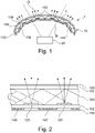
- Fig. 1 shows a cover 1, also referred to as a radome, for a radar sensor in accordance with the present invention.
- the cover 1 comprises a plate 10 that is arranged over a radar sensor 20, which comprises one or more radio transmitters and/or receivers or antennas in the conventional manner.
- the radio waves emitted and/or received are depicted as a cone R in Fig. 1 .
- the whole assembly can be attached to the front of a vehicle, for example, to a facia or grille of a vehicle.
- the plate 10 is a multilayer structure with a substantially even and constant thickness to ensure good radar performance.
- the geometry of the plate 10 is also devoid of abrupt changes or discontinuities for the same reason.
- the plate 10 is domed with a substantially uniform degree of curvature at least in a central portion that coincides with a radar cone R. It will be understood, however, that the plate may be substantially planar, over its whole structure, or at least in the central portion located above the radar cone R.
- the plate 10 includes a first layer 100 that serves as a light guide.
- Two light sources 130 are arranged at the outer rim of this first layer and arranged such that the light is coupled into the first layer 100.
- These light sources 130 preferably comprise one or more LEDs provided with associated power supply and control circuitry.
- the LEDs may be configured to generate white light or light of a specific colour.
- Two light sources 130 are illustrated in the figures, but it will be appreciated that a single light source or more than two light sources may be used.
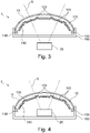
- Fig. 2 shows detailed view of the layered structure of the plate 10.
- second layers specifically optical insulating layers 110.
- These optical insulating layers 110 have a lower refractive index than the first layer 100 and thus ensure that light coupled into the first layer 100 is subjected to total internal reflection at the upper and lower surfaces of this layer 100 and thus propagates through it.
- the reflected light beams are illustrated in Figs. 1 and 2 as L.
- the optical insulating layer 110 serves to protect the light guide 100 from light leakage due to impurities that might deposit on the surface or graphic elements that could otherwise alter the refractive index boundary at the surface of the light guide 100.
- the second layer thus prevents unwanted glare for an observer and instead ensures that the cover 10 provides a homogenous background illumination.
- the optical insulating layers 102 are shown on both the upper and lower surfaces of the light guide 100, in some embodiments it may be sufficient to provide such an insulating layer only on the upper surface of the light guide 100, i.e. on the surface that is directly outwardly and is thus open to the elements, providing that the light guide 100 has a refractive index that is higher than air, i.e. higher than 1.
- the light guide 100 is made of a material that is substantially transparent to both light and to the radio waves used by the radar sensors. Suitable materials include thermoplastic polymers, such as polycarbonate (PC) or PMMA.
- the thickness of the light guide 100 depends on the application but is preferably within the range of 1 to 5 mm.
- the light guide 100 has a refractive index of between 1.3 and 1.6, preferably around 1.5.
- the optical insulating layer 110 is a thin film of depth between 1-6 ⁇ m, preferably between 2-3 ⁇ m and has a refractive index of less than 1.3, preferably 1.15 ⁇ 1.3.
- the optical insulating layer 110 is preferably substantially transparent to light and optically clear and also substantially transparent to the radio waves used by the radar sensors. Suitable materials include siloxane resins.
- the insulating layer or layers 110 may be spray-coated or otherwise deposited on the underlying layer 100, or alternatively bonded to this layer by adhesive or heat treatment.
- optical elements 120 are provided on the bottom surface of the first layer 100. These optical elements 120 serve to outcouple light from the light guide 100 by diffusing light, that is, by causing a refraction, reflection and/or diffraction of the light at the surface of first layer which causes it to leak out of the light guide 100. As a consequence, the plate 10 is perceived as illuminated, although the light sources 130 are not visible.
- These optical elements 120 may be composed of diffractive surface relief structures such as microstructures or a roughened or granular surface formed on the lower surface of the light guide, for example, by chemical or mechanical etching of the light guide surface.
- the optical elements 120 may alternatively be formed by applying a diffusing material to the light guide surface, or alternatively by incorporating a light-diffusing material in the light guide 100 by using a 2K injection moulding process.
- the optical elements 120 shown in Figs. 1 and 2 are provided only on the lower surface of the light guide 100, however, it will be understood that they may instead be provided on the upper surface, or equally on both the lower and upper surfaces of the light guide 100.
- the optical elements 120 may be provided as several discrete elements arranged in a regularly spaced pattern on the upper and/or lower surface of the light guide 100 to provide an even distribution of light over the surface of the cover plate 10.
- the optical elements 120 may formed as a single dispersing surface at a desired location on the light guide 100.
- the optical elements 120 may further be arranged to form a desired design, such as an emblem or logo, or the negative of a desired design, so that the observer will see an illuminated design or a shaded design.
- a graphic layer 140 comprising a film or foil, for example a metallic film or a foil on which a design is applied or that may be arranged to display a desired design such as the emblem or logo of a manufacturer.
- This film is preferably very thin, of the order of a few ⁇ m so that changes in thickness of the cover 10 between areas where the graphic layer is present and those where graphic material is absent have a negligible effect on the radiation emitted and/or received by the radar sensor 20.
- the material of the film 140 is substantially opaque and/or reflective to visible light, but substantially transparent to the electromagnetic radiation used by sensor 20. The design is visible through the multilayer structure of the light guide 100 and insulating layer 110.
- the graphic layer 140 may alternatively be formed on the upper surface of cover plate 10, i.e. on the outer surface of the upper insulating layer 110 (see Fig. 5 ), or even on the outer surface of both the upper and lower insulating layers 110. In all cases, the graphic layer 140 is separated from the first layer 100 by the optically insulating layer 110 to preclude the risk of light leakage that may otherwise occur on the boundary between the graphic layer 140 and first layer 100.
- the graphic layer 140 may advantageously be arranged to occupy the spaces between the optical elements 120 so that the design is visible not only by the presence of the graphic layer but also by the illuminated portions between the graphic elements. In this way, a desired shape may be displayed as an illuminated design or alternatively as the negative of an illuminated design.
- the cover plate 100 may also include an outer protective layer 150 applied to the upper and/or lower surface.
- This protective layer 150 is preferably a varnish or resin of sufficient hardness to protect the surface of the cover, and particularly the graphic layer 140, from wear and scratches.
- the protective layer 150 may be used to compensate for differences in thickness caused by the application or removal of the graphic layer. The protective layer 150 is omitted from the remaining figures in the interests of clarity.
- the cover 1 includes a frame 160 that extends downwards from the lower rim of cover plate 10 and under the cover plate 10 to enclose a space bordered by cover plate 10 and frame 160.
- the light sources 130 and associated electronics are located within this space.
- the frame 160 serves to block unwanted light and also protect the one or more light sources 130 and associated electronics.
- the frame 160 may also be provided with coupling elements, such as clips, screw holes or the like, that enable the cover 1 to be mounted over a radar sensor 20 on a vehicle, for example.
- the frame 160 is of a substantially optically opaque material, preferably of moulded plastic formed by injection moulding.
- the frame 160 may be fixed to the outer rim of the cover plate 10 by mechanical means, such as screws, rivets, clips, deformation of the frame 160, adhesive tape, or the like, chemical means, such as glue or lacquer, electromagnetic force using magnets, electric charge, or similar or by any other suitable fixing method.
- the cover 1 including the cover plate 10 and frame 160 may be arranged over a radar sensor 20, such that the radio waves illustrated by the cone R must pass through both the frame 160 and the cover plate 10.
- the frame 160 must be substantially transparent to the radio waves transmitted and/or received by the sensor 20.
- the spacing between the frame 160 and the cover plate 10, at least in the central area of the cover 1 that corresponds to the radio wave cone R, is chosen to minimise the attenuation of radio waves.
- the frame 160 does not extend over the whole space occupied by the plate 10 as shown in Fig. 3 , but instead covers only part of the way under the cover plate 10 such that the space is not enclosed, but the light sources 130 are protected and light leakage from the light sources 130 at the edge of the plate 10 are precluded or minimised.
- Fig. 4 shows a further embodiment of the cover 1.
- the radar sensor 20 is accommodated between the frame 160 and the cover plate 10, i.e. frame 160 and plate 10 together form a housing enclosing a protective space within which the radar sensor 20 light sources 130 and other electronic components may be accommodated..
- This arrangement reduces the attenuation of the radar signal as these pass through only two boundaries, namely the two outer surfaces of the cover plate 10.
- the frame 160 is essentially annular with an outer edge that essentially corresponds to that of the plate 10 or extends slightly beyond this, and an inner edge that extends inside the outer rim of the plate 10 to provide an essentially annular place serving as a protective housing for the light sources 130 and associated electronics.
- This annular space may be closed. In such an arrangement, the frame does not impact on the performance of the radar sensor 20 as it is not traversed by the conde R.
- Fig. 5 there is shown a further embodiment of the cover 1.
- the cover 1 illustrated in Fig. 5 is similar to that shown in Fig. 4 with the notable difference that a graphic layer 140 is provided on the upper side of the cover plate 10, i.e. on the outer surface of the upper optically insulating layer 110.
- a hardened protective layer 150 is preferably applied over the graphic layer, although this is not shown in Fig. 5 .
- the embodiment of Fig. 5 also includes an optically reflective layer 170 that is applied to a lower surface of the cover plate, specifically on the outer surface of the lower optically insulating layer 110. If a graphic layer 140 is present on the underside of the cover plate 10, the optically reflective layer 170 is applied over that layer, i.e.
- the optically reflective layer 170 serves to improve the efficiency and homogeneity of the illumination of the cover plate 10 by reflecting all light out of the cover plate 10.
- the layer 170 is preferably a white or pale film or coating, e.g. paint or pigmented lacquer of a few ⁇ m in thickness that is applied to the remaining structure of the cover plate 10 by adhesion or thermal bonding or another suitable manner.
- the optically reflective layer may also serve as a protective layer, or alternatively be coated with a protective layer 150
- Fig. 6 shows the steps of a process for manufacturing a cover plate 10 according to the embodiments described above.
- a first step designated a) the first light guide layer 100 is formed by injection moulding into the desired domed or planar shape of the cover plate 10.
- one or more optical elements are provided at the lower or upper surface of the light guide layer 100. These optical elements may be formed by mechanical means or chemical etching to create structured or roughened diffusing surfaces, or by application of a diffusing material to the surface of the layer 100 . Alternatively, the optical elements may be formed integrally with the light guide 100, for example by 2K injection moulding of a diffusing material and thus be formed simultaneously with step a).
- optical insulating layers 110 are applied to the upper and/or lower surfaces of the light guide layer 100. These optical insulating layers 110 may be applied directly to the surface of the light guide 100 and optionally hardened or cured, or applied as a separate film that is bonded to the surface of the light guide 100 by chemical or mechanical means.
- a graphic layer is applied to at least one of the outer surfaces formed by the optical insulating layers 110. This graphic layer 140 may be a metallization layer which is then partially removed to form the desired design by use of a laser or chemical etching. Alternatively, the graphic layer may be a foil on which a design is applied. The foil is then hot stamped to the optical insulating layer 110.
- the process may include further steps, for example the application of a protective layer 150 in the form of a lacquer, for example can be applied to the outer surface of the plate, but particularly over the graphic layer 140 to protect this and possibly compensate for variations in thickness.
- An optically reflective layer 170 may be applied prior to this step on the lower surface of the plate 10, i.e. on the surface that faces the radar sensor 20 and is directed away from the observer.
Landscapes
- Physics & Mathematics (AREA)
- General Physics & Mathematics (AREA)
- Engineering & Computer Science (AREA)
- Optics & Photonics (AREA)
- Radar, Positioning & Navigation (AREA)
- Remote Sensing (AREA)
- Computer Networks & Wireless Communication (AREA)
- Computer Security & Cryptography (AREA)
- Manufacturing & Machinery (AREA)
- Electromagnetism (AREA)
- Theoretical Computer Science (AREA)
- Laminated Bodies (AREA)
- Radar Systems Or Details Thereof (AREA)
- Mechanical Engineering (AREA)
- Illuminated Signs And Luminous Advertising (AREA)
- Optical Radar Systems And Details Thereof (AREA)
Priority Applications (7)
| Application Number | Priority Date | Filing Date | Title |
|---|---|---|---|
| EP21180398.6A EP4105678A1 (de) | 2021-06-18 | 2021-06-18 | Beleuchteter deckel für elektromagnetischen sender und empfänger |
| PCT/EP2022/066609 WO2022263655A1 (en) | 2021-06-18 | 2022-06-17 | Illuminated panel for automotive applications |
| CN202280043299.1A CN117501147A (zh) | 2021-06-18 | 2022-06-17 | 用于汽车应用的照明面板 |
| EP22730305.4A EP4356157A1 (de) | 2021-06-18 | 2022-06-17 | Leuchttafel für kraftfahrzeuganwendungen |
| US17/843,411 US20220404539A1 (en) | 2021-06-18 | 2022-06-17 | Illuminated cover for electromagnetic transmitter and receiver |
| CN202210691423.7A CN115494452A (zh) | 2021-06-18 | 2022-06-17 | 用于电磁发送器和接收器的照明盖子 |
| US18/541,180 US20240159957A1 (en) | 2021-06-18 | 2023-12-15 | Illuminated panel for automotive applications |
Applications Claiming Priority (1)
| Application Number | Priority Date | Filing Date | Title |
|---|---|---|---|
| EP21180398.6A EP4105678A1 (de) | 2021-06-18 | 2021-06-18 | Beleuchteter deckel für elektromagnetischen sender und empfänger |
Publications (1)
| Publication Number | Publication Date |
|---|---|
| EP4105678A1 true EP4105678A1 (de) | 2022-12-21 |
Family
ID=76532088
Family Applications (2)
| Application Number | Title | Priority Date | Filing Date |
|---|---|---|---|
| EP21180398.6A Pending EP4105678A1 (de) | 2021-06-18 | 2021-06-18 | Beleuchteter deckel für elektromagnetischen sender und empfänger |
| EP22730305.4A Pending EP4356157A1 (de) | 2021-06-18 | 2022-06-17 | Leuchttafel für kraftfahrzeuganwendungen |
Family Applications After (1)
| Application Number | Title | Priority Date | Filing Date |
|---|---|---|---|
| EP22730305.4A Pending EP4356157A1 (de) | 2021-06-18 | 2022-06-17 | Leuchttafel für kraftfahrzeuganwendungen |
Country Status (4)
| Country | Link |
|---|---|
| US (2) | US20220404539A1 (de) |
| EP (2) | EP4105678A1 (de) |
| CN (2) | CN115494452A (de) |
| WO (1) | WO2022263655A1 (de) |
Cited By (4)
| Publication number | Priority date | Publication date | Assignee | Title |
|---|---|---|---|---|
| DE102022120364A1 (de) * | 2022-08-11 | 2024-02-22 | Plastic Omnium Lighting Systems Gmbh | Lichtleiter mit Auskopplungsstruktur |
| WO2025040353A1 (de) * | 2023-08-22 | 2025-02-27 | Marelli Germany Gmbh | Beleuchtungseinrichtung, insbesondere für ein kraftfahrzeug |
| WO2025040485A1 (de) * | 2023-08-22 | 2025-02-27 | Marelli Germany Gmbh | Beleuchtungseinrichtung mit radartransparentem abschnitt und heizelement |
| DE102023125595B3 (de) | 2023-09-21 | 2025-03-20 | Motherson Innovations Company Limited | Lichtemittierendes system mit homogenem und diffusem licht; fahrzeug damit und herstellungsverfahren dafür |
Families Citing this family (8)
| Publication number | Priority date | Publication date | Assignee | Title |
|---|---|---|---|---|
| FR3099132B1 (fr) * | 2019-07-26 | 2022-01-28 | Mbda France | Capot pour vehicule, en particulier pour vehicule supersonique ou hypersonique |
| WO2021047772A1 (en) * | 2019-09-11 | 2021-03-18 | Hella Saturnus Slovenija d.o.o. | A device for attachment to an opening of a vehicle and for covering an emitter and/or a receiver |
| US12553989B2 (en) * | 2020-12-25 | 2026-02-17 | Nitto Denko Corporation | Radio wave scattering body, and member for attenuating radio waves comprising radio wave scattering body |
| EP4112290A1 (de) * | 2021-06-30 | 2023-01-04 | Volvo Car Corporation | Nahtlose integration von beleuchtung in innenverkleidungsplatten mit dekorativen oberflächenmaterialien |
| DE102021128982A1 (de) * | 2021-11-08 | 2023-05-11 | Marelli Automotive Lighting Reutlingen (Germany) GmbH | Sensorvorrichtung |
| US12332469B2 (en) * | 2022-01-11 | 2025-06-17 | Magna Electronics, Llc | Sensing system with side illumination |
| EP4369026A1 (de) * | 2022-11-10 | 2024-05-15 | Zanini Auto Grup, S.A. | Radom für fahrzeuge |
| US20250196762A1 (en) * | 2023-12-18 | 2025-06-19 | Valeo Vision | Optical component with micro-optical features |
Citations (9)
| Publication number | Priority date | Publication date | Assignee | Title |
|---|---|---|---|---|
| EP2383364A1 (de) * | 2009-01-20 | 2011-11-02 | Shin-Etsu Polymer Co. Ltd. | Radiowellen übertragendes schmuckelement sowie herstellungsverfahren dafür |
| WO2012130033A2 (zh) | 2011-03-29 | 2012-10-04 | 华为技术有限公司 | 电源装置及调节死区时间的方法 |
| DE102013016667A1 (de) * | 2013-10-08 | 2014-07-03 | Daimler Ag | Mehrlagiges Abdeckelement und Fahrzeugbauteil mit einem Abdeckelement |
| EP3300169A2 (de) | 2016-09-27 | 2018-03-28 | Faltec Co., Ltd. | Radarabdeckung und verfahren zur herstellung der radarabdeckung |
| EP3434473A1 (de) * | 2017-07-27 | 2019-01-30 | Zanini Auto Grup, S.A. | Emblem für fahrzeuge |
| DE102017214129A1 (de) * | 2017-08-14 | 2019-02-14 | Volkswagen Aktiengesellschaft | Radarfähiges Leuchtemblem für ein Fahrzeug |
| EP3495186A1 (de) | 2017-09-29 | 2019-06-12 | Intops. Co., Ltd. | Fahrzeugtempomatsensorabdeckung und herstellungsverfahren dafür |
| WO2020078916A2 (en) * | 2018-10-15 | 2020-04-23 | Motherson Innovations Company Ltd. | Decorative radome and method of producing the same |
| DE102018220997A1 (de) * | 2018-12-05 | 2020-06-10 | Volkswagen Aktiengesellschaft | Emblemanordnung für ein Kraftfahrzeug |
Family Cites Families (15)
| Publication number | Priority date | Publication date | Assignee | Title |
|---|---|---|---|---|
| KR20160105527A (ko) * | 2008-07-10 | 2016-09-06 | 쓰리엠 이노베이티브 프로퍼티즈 컴파니 | 점탄성 도광체 |
| CN103158633B (zh) * | 2011-12-19 | 2015-08-26 | 比亚迪股份有限公司 | 一种机动车车标 |
| KR20140064393A (ko) * | 2012-11-20 | 2014-05-28 | 서울반도체 주식회사 | 백라이트 유닛 |
| GB201306726D0 (en) * | 2013-04-12 | 2013-05-29 | Pilkington Group Ltd | A glazing |
| US9869810B2 (en) * | 2014-04-29 | 2018-01-16 | Tactotek Oy | Method for manufacturing electronic products, related arrangement and product |
| KR102616309B1 (ko) * | 2016-12-28 | 2023-12-20 | 자니니 오토 그룹 에스. 에이 | 차량용 레이돔 |
| KR102533078B1 (ko) * | 2017-06-16 | 2023-05-16 | 삼성디스플레이 주식회사 | 광학 부재 및 이를 포함하는 표시 장치 |
| JP6812936B2 (ja) * | 2017-09-22 | 2021-01-13 | 豊田合成株式会社 | 近赤外線センサ用カバー装置 |
| US11346523B2 (en) | 2018-03-13 | 2022-05-31 | Motherson Innovations Company Limited | Light emitting system, a design element, a rear view device, a covering device, and a body component of a vehicle |
| CN108873151B (zh) * | 2018-07-13 | 2020-05-15 | 京东方科技集团股份有限公司 | 导光板、制备导光板的方法以及显示装置 |
| EP4005022B1 (de) * | 2019-07-29 | 2025-09-17 | Motherson Innovations Company Limited | Erste oberfläche oder zweite oberfläche eines dekorativen radoms |
| EP4043909A1 (de) * | 2019-09-10 | 2022-08-17 | Koito Manufacturing Co., Ltd. | Leuchtenhalterung für fahrzeug, radarmodul, radar und fahrzeug |
| WO2021047772A1 (en) * | 2019-09-11 | 2021-03-18 | Hella Saturnus Slovenija d.o.o. | A device for attachment to an opening of a vehicle and for covering an emitter and/or a receiver |
| FR3105352B1 (fr) * | 2019-12-19 | 2022-03-04 | Valeo Vision | Elément lumineux d’un véhicule |
| US12004452B2 (en) * | 2020-10-29 | 2024-06-11 | Cnh Industrial America Llc | Radar-transparent components for headers of agricultural vehicles and related systems |
-
2021
- 2021-06-18 EP EP21180398.6A patent/EP4105678A1/de active Pending
-
2022
- 2022-06-17 CN CN202210691423.7A patent/CN115494452A/zh active Pending
- 2022-06-17 CN CN202280043299.1A patent/CN117501147A/zh active Pending
- 2022-06-17 WO PCT/EP2022/066609 patent/WO2022263655A1/en not_active Ceased
- 2022-06-17 US US17/843,411 patent/US20220404539A1/en not_active Abandoned
- 2022-06-17 EP EP22730305.4A patent/EP4356157A1/de active Pending
-
2023
- 2023-12-15 US US18/541,180 patent/US20240159957A1/en active Pending
Patent Citations (9)
| Publication number | Priority date | Publication date | Assignee | Title |
|---|---|---|---|---|
| EP2383364A1 (de) * | 2009-01-20 | 2011-11-02 | Shin-Etsu Polymer Co. Ltd. | Radiowellen übertragendes schmuckelement sowie herstellungsverfahren dafür |
| WO2012130033A2 (zh) | 2011-03-29 | 2012-10-04 | 华为技术有限公司 | 电源装置及调节死区时间的方法 |
| DE102013016667A1 (de) * | 2013-10-08 | 2014-07-03 | Daimler Ag | Mehrlagiges Abdeckelement und Fahrzeugbauteil mit einem Abdeckelement |
| EP3300169A2 (de) | 2016-09-27 | 2018-03-28 | Faltec Co., Ltd. | Radarabdeckung und verfahren zur herstellung der radarabdeckung |
| EP3434473A1 (de) * | 2017-07-27 | 2019-01-30 | Zanini Auto Grup, S.A. | Emblem für fahrzeuge |
| DE102017214129A1 (de) * | 2017-08-14 | 2019-02-14 | Volkswagen Aktiengesellschaft | Radarfähiges Leuchtemblem für ein Fahrzeug |
| EP3495186A1 (de) | 2017-09-29 | 2019-06-12 | Intops. Co., Ltd. | Fahrzeugtempomatsensorabdeckung und herstellungsverfahren dafür |
| WO2020078916A2 (en) * | 2018-10-15 | 2020-04-23 | Motherson Innovations Company Ltd. | Decorative radome and method of producing the same |
| DE102018220997A1 (de) * | 2018-12-05 | 2020-06-10 | Volkswagen Aktiengesellschaft | Emblemanordnung für ein Kraftfahrzeug |
Cited By (4)
| Publication number | Priority date | Publication date | Assignee | Title |
|---|---|---|---|---|
| DE102022120364A1 (de) * | 2022-08-11 | 2024-02-22 | Plastic Omnium Lighting Systems Gmbh | Lichtleiter mit Auskopplungsstruktur |
| WO2025040353A1 (de) * | 2023-08-22 | 2025-02-27 | Marelli Germany Gmbh | Beleuchtungseinrichtung, insbesondere für ein kraftfahrzeug |
| WO2025040485A1 (de) * | 2023-08-22 | 2025-02-27 | Marelli Germany Gmbh | Beleuchtungseinrichtung mit radartransparentem abschnitt und heizelement |
| DE102023125595B3 (de) | 2023-09-21 | 2025-03-20 | Motherson Innovations Company Limited | Lichtemittierendes system mit homogenem und diffusem licht; fahrzeug damit und herstellungsverfahren dafür |
Also Published As
| Publication number | Publication date |
|---|---|
| CN115494452A (zh) | 2022-12-20 |
| US20220404539A1 (en) | 2022-12-22 |
| CN117501147A (zh) | 2024-02-02 |
| US20240159957A1 (en) | 2024-05-16 |
| EP4356157A1 (de) | 2024-04-24 |
| WO2022263655A1 (en) | 2022-12-22 |
Similar Documents
| Publication | Publication Date | Title |
|---|---|---|
| US20220404539A1 (en) | Illuminated cover for electromagnetic transmitter and receiver | |
| EP3563449B1 (de) | Radom für fahrzeuge | |
| CN109305111B (zh) | 用于车辆的标志 | |
| KR101673035B1 (ko) | 레이돔의 제조 방법 | |
| EP2848474A1 (de) | Äußeres Fahrzeugelement | |
| US12286052B2 (en) | Light assembly, vehicle design element, rear view device and door finisher | |
| US20240162603A1 (en) | Radome for vehicles | |
| CN113544529A (zh) | 雷达罩 | |
| JP2019100792A (ja) | ライダーカバー | |
| EP3477185B1 (de) | Fahrzeuglampe und fahrzeug damit | |
| US20160046239A1 (en) | Rearview mirror with selective refelction and method of manufacture | |
| US20240356207A1 (en) | System for backlighting a radome and radar device | |
| JP2020036189A (ja) | レーダカバー及びレーダカバーの製造方法 | |
| US20230141051A1 (en) | Sensor Device | |
| JP2004309322A (ja) | レーダ装置の被覆部品 | |
| CN119999013A (zh) | 用于被照亮的标志的雷达透明结构 | |
| EP4439864B1 (de) | Radom für ein radargerät eines fahrzeugs, radargerät mit einem solchen radom, verkleidungsbauteil und fahrzeug mit einem solchen radargerät und/oder einem solchen verkleidungsbauteil | |
| KR20200126713A (ko) | 전파 송수신 레이더 전파 투과형 커버 | |
| US20240337363A1 (en) | Illuminated radome cover | |
| JP7852549B2 (ja) | 乗物用外装部品 | |
| KR102190898B1 (ko) | 전파 송수신 레이더 전파 투과형 커버 및 그 제조방법 | |
| CN120021098A (zh) | 车辆的或用于车辆的雷达装置用的天线罩、包括这种天线罩的雷达装置、具有这种雷达装置的包覆部件和车辆 | |
| CN121748785A (zh) | 天线罩、雷达装置以及装备有雷达装置的车辆 | |
| US20210116624A1 (en) | Front light module and display device | |
| CA2058180A1 (en) | Compact lighting panel |
Legal Events
| Date | Code | Title | Description |
|---|---|---|---|
| PUAI | Public reference made under article 153(3) epc to a published international application that has entered the european phase |
Free format text: ORIGINAL CODE: 0009012 |
|
| STAA | Information on the status of an ep patent application or granted ep patent |
Free format text: STATUS: THE APPLICATION HAS BEEN PUBLISHED |
|
| AK | Designated contracting states |
Kind code of ref document: A1 Designated state(s): AL AT BE BG CH CY CZ DE DK EE ES FI FR GB GR HR HU IE IS IT LI LT LU LV MC MK MT NL NO PL PT RO RS SE SI SK SM TR |
|
| STAA | Information on the status of an ep patent application or granted ep patent |
Free format text: STATUS: REQUEST FOR EXAMINATION WAS MADE |
|
| 17P | Request for examination filed |
Effective date: 20230616 |
|
| RBV | Designated contracting states (corrected) |
Designated state(s): AL AT BE BG CH CY CZ DE DK EE ES FI FR GB GR HR HU IE IS IT LI LT LU LV MC MK MT NL NO PL PT RO RS SE SI SK SM TR |
|
| STAA | Information on the status of an ep patent application or granted ep patent |
Free format text: STATUS: EXAMINATION IS IN PROGRESS |
|
| 17Q | First examination report despatched |
Effective date: 20250312 |