EP4105694A1 - Dispositif d'affichage, appareil électronique et procédé de production de dispositif d'affichage - Google Patents
Dispositif d'affichage, appareil électronique et procédé de production de dispositif d'affichage Download PDFInfo
- Publication number
- EP4105694A1 EP4105694A1 EP21753084.9A EP21753084A EP4105694A1 EP 4105694 A1 EP4105694 A1 EP 4105694A1 EP 21753084 A EP21753084 A EP 21753084A EP 4105694 A1 EP4105694 A1 EP 4105694A1
- Authority
- EP
- European Patent Office
- Prior art keywords
- film
- display
- display device
- transmittance
- display region
- Prior art date
- Legal status (The legal status is an assumption and is not a legal conclusion. Google has not performed a legal analysis and makes no representation as to the accuracy of the status listed.)
- Granted
Links
Images







Classifications
-
- H—ELECTRICITY
- H10—SEMICONDUCTOR DEVICES; ELECTRIC SOLID-STATE DEVICES NOT OTHERWISE PROVIDED FOR
- H10K—ORGANIC ELECTRIC SOLID-STATE DEVICES
- H10K77/00—Constructional details of devices covered by this subclass and not covered by groups H10K10/80, H10K30/80, H10K50/80 or H10K59/80
- H10K77/10—Substrates, e.g. flexible substrates
-
- H—ELECTRICITY
- H10—SEMICONDUCTOR DEVICES; ELECTRIC SOLID-STATE DEVICES NOT OTHERWISE PROVIDED FOR
- H10K—ORGANIC ELECTRIC SOLID-STATE DEVICES
- H10K59/00—Integrated devices, or assemblies of multiple devices, comprising at least one organic light-emitting element covered by group H10K50/00
- H10K59/60—OLEDs integrated with inorganic light-sensitive elements, e.g. with inorganic solar cells or inorganic photodiodes
-
- G—PHYSICS
- G02—OPTICS
- G02B—OPTICAL ELEMENTS, SYSTEMS OR APPARATUS
- G02B1/00—Optical elements characterised by the material of which they are made; Optical coatings for optical elements
- G02B1/10—Optical coatings produced by application to, or surface treatment of, optical elements
- G02B1/11—Anti-reflection coatings
- G02B1/118—Anti-reflection coatings having sub-optical wavelength surface structures designed to provide an enhanced transmittance, e.g. moth-eye structures
-
- G—PHYSICS
- G02—OPTICS
- G02B—OPTICAL ELEMENTS, SYSTEMS OR APPARATUS
- G02B27/00—Optical systems or apparatus not provided for by any of the groups G02B1/00 - G02B26/00, G02B30/00
- G02B27/01—Head-up displays
-
- G—PHYSICS
- G02—OPTICS
- G02B—OPTICAL ELEMENTS, SYSTEMS OR APPARATUS
- G02B5/00—Optical elements other than lenses
- G02B5/20—Filters
- G02B5/208—Filters for use with infrared or ultraviolet radiation, e.g. for separating visible light from infrared and/or ultraviolet radiation
-
- H—ELECTRICITY
- H10—SEMICONDUCTOR DEVICES; ELECTRIC SOLID-STATE DEVICES NOT OTHERWISE PROVIDED FOR
- H10K—ORGANIC ELECTRIC SOLID-STATE DEVICES
- H10K59/00—Integrated devices, or assemblies of multiple devices, comprising at least one organic light-emitting element covered by group H10K50/00
- H10K59/40—OLEDs integrated with touch screens
-
- H—ELECTRICITY
- H10—SEMICONDUCTOR DEVICES; ELECTRIC SOLID-STATE DEVICES NOT OTHERWISE PROVIDED FOR
- H10K—ORGANIC ELECTRIC SOLID-STATE DEVICES
- H10K59/00—Integrated devices, or assemblies of multiple devices, comprising at least one organic light-emitting element covered by group H10K50/00
- H10K59/60—OLEDs integrated with inorganic light-sensitive elements, e.g. with inorganic solar cells or inorganic photodiodes
- H10K59/65—OLEDs integrated with inorganic image sensors
-
- H—ELECTRICITY
- H10—SEMICONDUCTOR DEVICES; ELECTRIC SOLID-STATE DEVICES NOT OTHERWISE PROVIDED FOR
- H10K—ORGANIC ELECTRIC SOLID-STATE DEVICES
- H10K59/00—Integrated devices, or assemblies of multiple devices, comprising at least one organic light-emitting element covered by group H10K50/00
- H10K59/80—Constructional details
- H10K59/87—Passivation; Containers; Encapsulations
- H10K59/873—Encapsulations
-
- H—ELECTRICITY
- H10—SEMICONDUCTOR DEVICES; ELECTRIC SOLID-STATE DEVICES NOT OTHERWISE PROVIDED FOR
- H10K—ORGANIC ELECTRIC SOLID-STATE DEVICES
- H10K71/00—Manufacture or treatment specially adapted for the organic devices covered by this subclass
-
- H—ELECTRICITY
- H10—SEMICONDUCTOR DEVICES; ELECTRIC SOLID-STATE DEVICES NOT OTHERWISE PROVIDED FOR
- H10K—ORGANIC ELECTRIC SOLID-STATE DEVICES
- H10K71/00—Manufacture or treatment specially adapted for the organic devices covered by this subclass
- H10K71/80—Manufacture or treatment specially adapted for the organic devices covered by this subclass using temporary substrates
-
- H—ELECTRICITY
- H10—SEMICONDUCTOR DEVICES; ELECTRIC SOLID-STATE DEVICES NOT OTHERWISE PROVIDED FOR
- H10K—ORGANIC ELECTRIC SOLID-STATE DEVICES
- H10K77/00—Constructional details of devices covered by this subclass and not covered by groups H10K10/80, H10K30/80, H10K50/80 or H10K59/80
- H10K77/10—Substrates, e.g. flexible substrates
- H10K77/111—Flexible substrates
-
- G—PHYSICS
- G02—OPTICS
- G02B—OPTICAL ELEMENTS, SYSTEMS OR APPARATUS
- G02B27/00—Optical systems or apparatus not provided for by any of the groups G02B1/00 - G02B26/00, G02B30/00
- G02B27/01—Head-up displays
- G02B27/0101—Head-up displays characterised by optical features
- G02B2027/0138—Head-up displays characterised by optical features comprising image capture systems, e.g. camera
-
- G—PHYSICS
- G06—COMPUTING OR CALCULATING; COUNTING
- G06V—IMAGE OR VIDEO RECOGNITION OR UNDERSTANDING
- G06V40/00—Recognition of biometric, human-related or animal-related patterns in image or video data
- G06V40/10—Human or animal bodies, e.g. vehicle occupants or pedestrians; Body parts, e.g. hands
- G06V40/12—Fingerprints or palmprints
- G06V40/13—Sensors therefor
- G06V40/1318—Sensors therefor using electro-optical elements or layers, e.g. electroluminescent sensing
-
- H—ELECTRICITY
- H04—ELECTRIC COMMUNICATION TECHNIQUE
- H04N—PICTORIAL COMMUNICATION, e.g. TELEVISION
- H04N23/00—Cameras or camera modules comprising electronic image sensors; Control thereof
- H04N23/57—Mechanical or electrical details of cameras or camera modules specially adapted for being embedded in other devices
-
- Y—GENERAL TAGGING OF NEW TECHNOLOGICAL DEVELOPMENTS; GENERAL TAGGING OF CROSS-SECTIONAL TECHNOLOGIES SPANNING OVER SEVERAL SECTIONS OF THE IPC; TECHNICAL SUBJECTS COVERED BY FORMER USPC CROSS-REFERENCE ART COLLECTIONS [XRACs] AND DIGESTS
- Y02—TECHNOLOGIES OR APPLICATIONS FOR MITIGATION OR ADAPTATION AGAINST CLIMATE CHANGE
- Y02E—REDUCTION OF GREENHOUSE GAS [GHG] EMISSIONS, RELATED TO ENERGY GENERATION, TRANSMISSION OR DISTRIBUTION
- Y02E10/00—Energy generation through renewable energy sources
- Y02E10/50—Photovoltaic [PV] energy
- Y02E10/549—Organic PV cells
-
- Y—GENERAL TAGGING OF NEW TECHNOLOGICAL DEVELOPMENTS; GENERAL TAGGING OF CROSS-SECTIONAL TECHNOLOGIES SPANNING OVER SEVERAL SECTIONS OF THE IPC; TECHNICAL SUBJECTS COVERED BY FORMER USPC CROSS-REFERENCE ART COLLECTIONS [XRACs] AND DIGESTS
- Y02—TECHNOLOGIES OR APPLICATIONS FOR MITIGATION OR ADAPTATION AGAINST CLIMATE CHANGE
- Y02P—CLIMATE CHANGE MITIGATION TECHNOLOGIES IN THE PRODUCTION OR PROCESSING OF GOODS
- Y02P70/00—Climate change mitigation technologies in the production process for final industrial or consumer products
- Y02P70/50—Manufacturing or production processes characterised by the final manufactured product
Definitions
- the present disclosure relates to a display device, an electronic apparatus, and a method for manufacturing the display device.
- the frame (bezel) of its display panel is equipped with various sensors such as a camera.
- various sensors such as a camera.
- a technique has been proposed in which a camera module is disposed immediately below the display panel and subject light passed through the display panel is shot by the camera module.
- Patent Document 1 US Patent Publication No. 2018/0069060
- a sealing material for preventing moisture or the like from intruding from the outside is required for a display panel, and polyimide is typically used for the sealing material.
- Polyimide is also excellent in heat resistance, and can withstand a heat treatment process in formation of a thin film transistor (TFT).
- Polyimide is low in transmittance to visible light.
- the shooting image quality deteriorates.
- the present disclosure provides a display device, an electronic apparatus, and a method for manufacturing the display device that enable improvement in transmittance without impairing display quality.
- a display device including: a substrate;
- the second display region may face a sensing device disposed on a side of a face opposite to a display face on the substrate.
- the display device may further include: a first film disposed on the side of the face opposite to the display face within the first display region, the first film having the first transmittance.
- the display device may further include: a second film disposed on the side of the face opposite to the display face within the second display region, the second film having the second transmittance.
- the second film may be disposed on the side of the face opposite to the display face in at least part of the second display region, the part including a boundary portion between adjacent pixels within the second display region.
- a ratio of an area of the second film to an area of a light emitting region within the second display region may be 30% or more.
- the second film may have a function of cutting infrared light.
- the second film may be disposed at an opening formed by removal of part of the first film, and a transmittance of a boundary portion between the first film and the second film may vary continuously or stepwise from the first film to the second film.
- the first film may contain polyimide
- the second film may contain a material higher in transmittance than the polyimide of the first film.
- the second film may have at least one of a concave portion or a convex portion.
- the display device may further include: an optical lens including the second film.
- the display device may further include: a moth-eye structure layer including the second film.
- the first film may be provided in at least part of the second display region, the at least part excluding a boundary portion between adjacent pixels within the second display region, and an opening of the first film may be provided at the boundary portion between the adjacent pixels within the second display region.
- the first transmittance to visible light having a wavelength of 400 nm may be 0 to 50%, and the second transmittance to the visible light may be 51 to 100%.
- an electronic apparatus including: a display device;
- the sensing device may include an imaging sensor.
- the sensing device may include a biometric-information detection sensor.
- a plurality of the second display regions may be provided on the display face, and a plurality of the sensing devices may be disposed corresponding to the plurality of the second display regions.
- the respective second transmittances of at least two of the plurality of the second display regions may be different from each other.
- a method for manufacturing a display device comprising:
- the method may further include: forming a second film at the opening, the second film having a second transmittance higher than the first transmittance.
- a manufacturing method comprising:
- the method may further include: forming a second film at the opening formed by the removing, the second film being higher in transmittance than the first film.
- a display device 1 may have components and functions that are not illustrated or described. The following description does not exclude the components and functions that are not illustrated or described.
- Fig. 1 is a schematic external view of an electronic apparatus 2 equipped with a display device 1 according to a first embodiment.
- the electronic apparatus 2 in Fig. 1 is any electronic apparatus 2 having both a display function and a shooting function, such as a smartphone, a mobile phone, a tablet, or a PC.
- the electronic apparatus 2 in Fig. 1 includes a camera module (imaging unit) 3 disposed opposite a display face 1a of the display device 1.
- the disposition place of the camera module 3 is indicated by a broken line.
- the camera module 3 is provided on the rear side of the display face 1a of the display device 1. Therefore, the camera module 3 performs imaging through the display device 1.
- the display face 1a side of the display device 1 is referred to as a front face
- the side on which the camera module 3 is disposed is referred to as a rear face.
- the transmittance of part of the display region overlapping the disposition place of the camera module 3 on the rear face side of the display device 1 is increased.
- the display device 1 includes a first display region D1 and a second display region D2 disposed on a substrate.
- the substrate has a first transmittance.
- the substrate has a second transmittance higher than the first transmittance.
- the second display region D2 may face a sensing device such as the camera module 3 disposed on the side of the face opposite to the display face on the substrate.
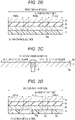
- Fig. 2A is a schematic sectional view illustrating part of the second display region D2.
- Fig. 2B is a schematic sectional view illustrating part of the first display region D1.
- Fig. 2C is a schematic sectional view of the display device 1 including the first display region D1 and the second display region D2.
- Figs. 2A and 2B each illustrate the region including three adjacent pixels.
- Each pixel has an upper electrode 4, a light emitting layer 5, and a lower electrode 6.
- a pixel has a complicated layered configuration, but is illustrated in a simplified manner in Figs. 2A and 2B .
- the upper face in Figs. 2A and 2B is the display face 1a, and the camera module 3 is disposed on the lower face side.
- a base film 7 is disposed under the lower electrode 6 in the first display region D1.
- the base film 7 includes opaque polyimide low in transmittance. Due to the low transmittance of the base film 7, light from the display face 1a side is blocked by the base film 7, resulting in a decrease in the amount of incident light to the camera module 3. Therefore, in the present embodiment, the base film 7 is not disposed under the lower electrode 6 in the second display region D2 as illustrated in Fig. 2A . In Figs. 2A and 2B , the base film 7 is referred to as a first film 7b.
- FIG. 2A illustrates an example in which a second film 7c higher in transmittance than the base film 7 (first film 7b) is disposed under the lower electrode 6 in the second display region D2.
- the second display region D2 faces the camera module 3 disposed on the side of the face 1b opposite to the display face 1a on the substrate of the display device 1.
- Fig. 2B illustrates the example in which the second film 7c is disposed under the lower electrode 6 over the entirety of the second display region D2.
- the first film 7b may be disposed under the lower electrode 6 in the second display region D2
- an opening 7a may be partially provided at the first film 7b
- the second film 7c may be disposed within the opening 7a.
- the second film 7c in Fig. 2D is disposed on the side of the face 1b opposite to the display face 1a in at least part of the second display region D2, and the part includes a boundary portion between adjacent pixels within the second display region D2.
- the opening 7a is provided at least at a boundary portion between pixels.
- the ratio of the area of the opening 7a or the second film 7c to the area of the light emitting region within the second display region D2 is desirably 30% or more.
- the second film 7c may have a function of cutting infrared light. Further, the transmittance of the boundary portion between the first film 7b and the second film 7c may vary continuously or stepwise from the first film 7b to the second film 7c.
- the first transmittance to visible light having a wavelength of 400 nm is 0 to 50%, for example.
- the second transmittance to the visible light is 51 to 100%, for example.
- the base film 7 is also disposed at the boundary portion between pixels, and no opening is provided.
- This arrangement enables a further increase in the transmittance on the camera module 3 side of the second display region D2 overlapping the disposition place of the camera module 3 and an increase in the amount of incident light to the camera module 3. As a result, the image quality of a shot image can be improved.
- the display device 1 according to the present embodiment is characterized in that the transmittance on the camera module 3 side of the second display region D2 is further increased.
- the display device 1 according to the present embodiment is applicable to a display device 1 including an organic electroluminescence (EL) element that performs self-light emission, and is also applicable to a liquid crystal display device 1.
- EL organic electroluminescence
- a normal camera module 3 mainly images visible light
- anything low in transmittance to visible light is often referred to as being opaque.
- the camera module 3 disposed on the rear face side of the display device 1 images, for example, infrared light
- anything low in transmittance to infrared light is opaque.
- the transparent or opaque level and the value of the transmittance are determined in consideration of a balance with the wavelength of light to which the camera module 3 disposed on the rear face side of the display device 1 has detection sensitivity.
- the camera module 3 for detecting or imaging visible light is disposed on the rear face side of the display device 1
- anything high in transmittance to visible light is referred to as being transparent
- anything low in transmittance to visible light is referred to as being opaque.
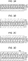
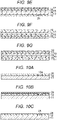
- Figs. 3A to 3F are sectional views illustrating a manufacturing process of the display device 1 according to the first embodiment.
- Figs. 3A to 3F each illustrate a sectional structure of part of the second display region D2 in Fig. 2 .
- Figs. 3A to 3F each illustrate a layered configuration related to the characteristic portion of the display device 1 according to the present embodiment, and there may be a layer not illustrated in the actual display device 1.
- most of the recent display devices 1 adopt a touch panel type, and a touch sensor layer is provided in the layered configuration of such a display device 1 as above, but is not given in Figs. 3A to 3F .
- Figs. 3A to 3F are sectional views illustrating a manufacturing process of the display device 1 according to the first embodiment.
- Figs. 3A to 3F each illustrate a sectional structure of part of the second display region D2 in Fig. 2 .
- Figs. 3A to 3F each illustrate a layered configuration related to
- the light emitting layer 5 that causes the organic EL element to emit light is illustrated as an EL layer 15
- the light emitting layer 5 can include a plurality of layers in practice.
- a plurality of TFTs that controls light emission of the organic EL element is illustrated as a TFT layer 14
- the TFT layer 14 can include a plurality of layers in practice.
- a base film 12, a first protective film 13, a TFT layer 14, an EL layer 15, a second protective film 16, and transparent film 17 are formed in this order on a glass substrate 11.
- the base film 12 functions as a sealing material, and usually includes opaque polyimide excellent in heat resistance.
- the first protective film 13 includes an insulating film high in transmissivity, such as SiN or SiO 2 .
- the TFT layer 14 is formed by implanting impurity ions into, for example, the drain region and the source region, and thermally diffusing the impurity ions.
- the EL layer 15 includes a plurality of layers such as an electron injection layer, an electron import layer, a light emitting layer 5, a hole transport layer, a charge generation layer, and an electron import layer.
- the second protective film 16 includes an insulating film high in transmissivity, such as SiN or SiO 2 .
- the step of Fig. 3A is the same as that of a normal organic EL display device 1.
- the opaque layer is the base film 12, and the other layers (excluding a sacrificial layer) each include a material higher in transmittance than the base film 12.
- a glass substrate 19 is formed above the transparent film 17 with the sacrificial layer 18 interposed therebetween.
- the sacrificial layer 18 is provided for absorbing laser light to facilitate peeling of the glass substrate 19 in peeling of the glass substrate 19 by laser lift-off in a later step.
- the glass substrate 11 on the base film 12 is removed to expose the base film 12.
- the glass substrate 11 may be removed by backgrinding (BGR) or chemical mechanical polishing (CMP).
- BGR backgrinding
- CMP chemical mechanical polishing
- the glass substrate 11 may be peeled off by laser lift-off.
- a resist 10 is applied onto the exposed base film 12 with the front and rear sides reversed, and then the resist 10 is patterned by lithography. More specifically, an opening 12a is provided at the resist 10 so as to be coincident with the disposition place of a camera module 3. Then, using the resist 10 as a mask, part of the base film 12 at the opening 12a of the resist 10 is etched.
- the resist 10 is peeled off to expose the base film 12.
- the opening 12a is formed at the part of the base film 12 (region overlapping the disposition place of the camera module 3) is cut by the etching and the opening 12a is formed.
- a transmissive member 20 is formed at the opening 12a.
- the transmissive member 20 may be, for example, transparent polyimide. Note that the transmissive member 20 corresponds to the second film 7c and the base film 12 corresponds to the first film 7b in Fig. 2 .
- transparent polyimide is often inferior in heat resistance to the existing opaque polyimide.
- the portion overlapping the camera module 3 includes transparent polyimide. Because the base film 12 itself has heat resistance, a diffusion process can be performed with high heat. Thus, there is no possibility that the electrical characteristics of the TFT formed in the TFT layer 14 are deteriorated.
- the glass substrate 19 is peeled off by laser lift-off.
- the laser light emitted to the glass substrate 19 is absorbed by the sacrificial layer 18, and the glass substrate 19 formed on the sacrificial layer 18 can be easily peeled off.
- a flexible substrate-shaped display device 1 excellent in flexibility is obtained. Because the display device 1 can be used in a curved shape, its utility value is increased.
- the camera module 3 can be attached facing the transmissive member 20 formed at the part of the base film 12.
- various sensor modules other than the camera module 3 may be attached to the rear face side of the display device 1 according to the present embodiment.
- various biometric-information detection sensors such as a fingerprint sensor may be disposed facing the transmissive member 20 at the base film 12.
- structure bodies including the camera module 3 that perform any type of sensing will be collectively referred to as a sensing device.
- the transmittance (second transmittance) on the sensing device side of the transmissive member 20 formed at the part of the base film 12 is higher than the transmittance (first transmittance) on the sensing device side of the base film 12.
- the transmissive member 20 formed at the part of the base film 12 can be formed at a boundary portion between pixels of the display device 1.
- a display region not facing the sensing device is referred to as a first display region D1
- a display region facing the sensing device is referred to as a second display region D2.
- the transmittance on the side of the face opposite to a display face 1a in the first display region D1 is the first transmittance
- the transmittance on the side of the face (sensing device side) opposite to the display face 1a in the second display region D2 is the second transmittance higher than the first transmittance
- the transmissive member 20 may have not only higher transmittance than the base film 12 but also a function of cutting infrared light. If the transmissive member 20 has a function of cutting infrared light, it is not necessary to provide an infrared-light cut film or the like on the sensing device side, so that the configuration of the sensing device can be simplified.
- the transmittance of the boundary portion between the base film 12 and the transmissive member 20 may vary continuously or stepwise from the base film 12 to the transmissive member 20.
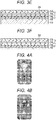
- a location low in transmittance is represented in black.
- Fig. 4A illustrates an example in which the density of a region low in transmittance increases stepwise from the center to the peripheral edge of the transmissive member 20.
- Fig. 4B illustrates an example in which the transmittance continuously varies from the center to the peripheral edge of the transmissive member 20.
- a lens for the camera module 3 can be formed at the transmissive member 20 manufactured in the steps of Figs. 3A to 3E .
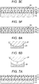
- Figs. 5A to 5F are sectional views illustrating a process of forming a lens at the transmissive member 20.
- Fig. 5A illustrates a sectional structure similar to that in Fig. 3E .
- part of the transmissive member 20 formed at the part of the base film 12 is removed to form a concave portion 20a.
- the concave portion 20a can be formed by, for example, etching or imprinting.
- Figs. 6A and 6B are explanatory views schematically illustrating an exemplary procedure of an imprinting process.
- the front face of the transmissive member 20 is subjected to heating or is irradiated with light, so that the outer shape of the master plate 21 is transferred to the transmissive member 20.
- the master plate 21 is released, and heat treatment, light irradiation, or the like is performed.
- the front-face shape of the transmissive member 20 can be formed into a shape corresponding to the outer shape of a lens.
- the imprinting process is performed to form at least one of a concave portion or a convex portion on the front face of the transmissive member 20.
- a transparent resin layer 22 is formed on the base film 12 including the inside of the above concave portion 20a in a process similar to a manufacturing process of an on-chip lens of a complementary metal oxide semiconductor (CMOS) image sensor.
- CMOS complementary metal oxide semiconductor
- a resist 23 is applied onto the transparent resin layer 22 and patterned to leave the resist 23 only immediately above the transmissive member 20.
- the transparent resin layer 22 is partially removed by etching using the resist 23 as a mask, and then the resist 23 is removed.
- a lens 24 includes the transparent resin layer 22 at the part of the transmissive member 20.
- the lens 24 is, for example, a convex lens.
- the transmissive member 20 is subjected to the front-face processing in Fig. 5B and the resist 23 is patterned in Fig. 5D so as to fit the outer shape of the lens 24.
- a lens having a desired outer shape can be formed.
- the glass substrate 19 is peeled off by, for example, laser lift-off, so that a flexible substrate-shaped display device 1 with the lens is obtained.
- This lens can be used to collect light to a sensing device such as the camera module 3.
- the transmissive member 20 can be processed into various shapes by using, for example, an imprinting process.
- the transmissive member 20 can also be processed to form a moth-eye structure layer having fine bumps.
- the moth-eye structure layer has a function of suppressing reflection.
- the amount of incident light to the lens can be increased and a shot image quality can be improved.
- the opening 12a is provided at the part of the base film 12 including opaque polyimide so as to be coincident with the disposition place of the sensing device such as the camera module 3, and the transmissive member 20 is formed at the opening 12a. Therefore, sufficient light can be guided to the sensing device through the transmissive member 20, so that the detection sensitivity of the sensing device can be improved.
- the transmissive member 20 is formed at the opening 12a formed at the part of the base film 12, but the opening 12a may be left. Even if the opening 12a is left, that is, the transmissive member 20 is not disposed inside the opening 12a, the transmittance on the sensing device side of the opening 12a is higher than the transmittance on the sensing device side of the base film 12. Therefore, due to disposition of the sensing device facing the opening 12a, the amount of incident light to the sensing device is increased.
- Figs. 7A to 7F are sectional views illustrating a manufacturing process of a display device 1 according to a second embodiment.
- Figs. 7A to 7D are the same as Figs. 3A to 3D .
- the opening 12a is formed at the exposed base film 12 so as to be coincident with the disposition place of the sensing device, and the transmissive member 20 is formed at the opening 12a.
- an opening 12a is formed and left, and a transmissive member 20 is not formed within the opening 12a.
- a glass substrate 19 is peeled off by laser lift-off, so that a flexible substrate-shaped display device 1 excellent in flexibility can be obtained.
- a sensing device such as a camera module 3 may be disposed facing the opening 12a formed at part of the base film 12, or in order to protect a base film 12, the front face of the base film 12 may be covered with a protective film having transmissivity while leaving the opening 12a.
- the opening 12a becomes a void sealed with the base film 12 and the protective film, so that high transmissivity is maintained.
- the opening 12a is formed at the part of the base film 12 so as to be coincident with the disposition place of the sensing device. Thus, sufficient light can be incident to the sensing device through the opening 12a. Because the step of forming another member at the opening 12a can be omitted, the manufacturing process can be simplified as compared with the first embodiment.
- a base film 12 including polyimide is removed after the process of applying heat in fabrication of a display device 1 is completed.
- the reason for using opaque polyimide as the base film 12 of a display device 1 is that opaque polyimide is excellent in heat resistance.
- heat treatment is performed.
- transparent polyimide is used as a base film 12
- too high heat cannot be applied thereto.
- electrical characteristics of the TFT are deteriorated.
- the base film 12 using opaque polyimide is formed until the step of applying heat in the fabrication of the display device 1 is completed, and the base film 12 is peeled off after the step of applying heat is completed.
- Figs. 8A to 8F are sectional views illustrating a manufacturing process of the display device 1 according to the third embodiment.
- Figs. 8A to 8C are the same as Figs. 3A to 3C .
- Fig. 8D at the stage where a glass substrate 11 is removed (peeled off) to expose the base film 12, a TFT layer 14 and an EL layer 15 are already formed. Thus, there is no subsequent step of applying high heat. Therefore, as illustrated in Fig. 8E , the base film 12 is removed by etching or the like. At this time, a protective film including, for example, SiN is used as an etching stopper layer.
- a glass substrate 19 is peeled off by laser lift-off.
- a transparent resin layer 22 or the like may be disposed on the protective film.
- the base film 12 including opaque polyimide is formed until the step of applying heat in the fabrication of the display device 1 is completed, and the base film 12 is removed after the step of applying heat is completed.
- the transmittance of the entirety of a second display region D2 can be increased, so that sufficient light can be incident to a sensing device.
- a fourth embodiment is different from the first to third embodiments in the order of steps of forming an opening 12a at part of a base film 12.
- Figs. 9A to 9G are sectional views illustrating a manufacturing process of a display device 1 according to the fourth embodiment.
- the base film 12 including opaque polyimide is formed on a glass substrate 11, and then the opening 12a is formed at the base film 12 so as to be coincident with the disposition place of a sensing device.
- a resist is applied onto the base film 12 and patterned, and the opening 12a is formed by etching.
- the upper face of the base film 12 including the inside of the opening 12a is covered with an insulating film 25 high in transmissivity, such as SiO 2 or SiN.
- the insulating film 25 formed on the upper face of the base film 12 is removed by, for example, CMP to expose the base film 12 and the insulating film 25 within the opening 12a.
- a first protective film 13, a TFT layer 14, an EL layer 15, a second protective film 16, and a transparent film 17 are formed in this order on the base film 12.
- the glass substrate 11 is removed (peeled off) by, for example, etching or laser lift-off to expose the base film 12.
- the insulating film 25 formed inside the opening 12a of the base film 12 is removed by, for example, etching.
- the second protective film 16 under the base film 12 functions as an etching stopper layer.
- the opening 12a is formed within the base film 12 at the initial stage of the manufacturing process of the display device 1.
- the layers of the display device 1 are each formed in the above order.
- the insulating film 25 within the opening 12a is replaced with the original transmissive member 20.
- the insulating film 25 is removed by, for example, CMP to expose the base film 12 and the insulating film 25 within the opening 12a.
- a stopper layer may be provided in advance on the upper face of the base film 12.
- Figs. 10A to 10C are sectional views of steps performed instead of those of Figs. 9B and 9C .
- an opening 12a is formed at part of a base film 12.
- the upper face of the base film 12 including an inner wall portion of the opening 12a is covered with a stopper layer 26.
- the stopper layer 26 is formed by, for example, atomic layer deposition (ALD), or chemical vapor deposition (CVD).
- an insulating film 25 is formed on the stopper layer 26.
- the insulating film 25 on the stopper layer 26 is removed by etching to expose the stopper layer 26 and the insulating layer 25 within the opening 12a.
- the opening 12a is formed at the base film 12 at the initial stage of the manufacturing process of the display device 1.
- the opening 12a can be formed easily.
- the temporary insulating film 25 high in heat resistance is formed at the opening 12a and the insulating film 25 is replaced with the transmissive member 20 at the final stage.
- high heat can be applied at the time of manufacturing the display device 1, so that the display device 1 excellent in electrical characteristics can be fabricated.
- various sensing devices can be disposed facing the opening 12a formed at the part of the base film 12.
- a fingerprint sensor that does not require a lens is disposed will be described as an exemplary sensing device for detecting biometric information.
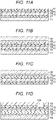
- Figs 11A to 11J are sectional views illustrating a manufacturing process of a display device 1 according to a fifth embodiment.
- Figs. 11A to 11E are similar to Figs. 7A to 7E .
- a fingerprint sensor 31 is disposed.
- the opening size of an opening 12a formed at part of a base film 12 is a size in agreement with the outer shape of the fingerprint sensor 31. More specifically, the opening size of the opening 12a needs to be larger than the outer size of the fingerprint sensor 31.
- the fingerprint sensor 31 is formed within the opening 12a formed at the part of the base film 12.
- the fingerprint sensor 31 does not require a lens on its outside, but an inner lens 31a is provided inside the fingerprint sensor 31.
- the opening size of the opening 12a formed at the part of the base film 12 is larger than the outer size of the fingerprint sensor 31.
- a gap is formed between the inner wall face of the opening 12a and the outer wall face of the fingerprint sensor 31. Therefore, as illustrated in Fig. 11G , an adhesive layer or an insulating film 32 is formed on the entire upper face of the base film 12 including the gap.
- the insulating film 32 in this case is, for example, SiO 2 or SiN.
- the adhesive layer or the insulating film 32 is removed by, for example, CMP or etching to expose the base film 12.
- the adhesive layer or the insulating film 32 fills between the inner wall face of the opening 12a and the outer wall face of the fingerprint sensor 31.
- a bonding wire 34 is connected to the pad portion 33 of the fingerprint sensor 31 to make wiring connection.
- the sensing device can be directly disposed at the opening 12a formed at the part of the base film 12.
- a plurality of sensing devices is disposed opposite a display face 1a of a display device 1.
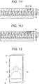
- Fig. 12 is a plan view of an electronic apparatus 2 according to the sixth embodiment.
- three sensing devices 30 are disposed opposite the display face 1a of the display device 1.
- the number of sensing devices 30 is not limited to three.
- a target to be sensed by such a sensing device 30 described above is optional.
- all the three sensing devices 30 may be camera modules and different in focal length.
- a camera module and two biometric-information-detection sensing devices may be disposed in combination.
- An opening 12a is formed at a base film 12 of the display device 1 corresponding to each of the sensing devices 30.
- a transmissive member 20 may be disposed at the opening 12a, or may be left. There is a possibility that the optimum light amount of incident light differs depending on the type of a sensing device 30. Thus, in order to dispose a transmissive member 20 at the opening 12a, it is desirable to set the transmittance of the transmissive member 20 to a value corresponding to each sensing device 30.
- the plurality of types of sensing devices 30 is disposed on the rear face side of the display device 1, and the transmittance of the transmissive member 20 disposed at a place overlapping each sensing device 30 is optimized individually. As a result, the detection sensitivity of all the sensing devices 30 can be improved.
- an optical system of a camera module 3 is different from those of the first to sixth embodiments.
- Fig. 13 illustrates a sectional structure of an imaging unit of the camera module 3 with which the electronic apparatus 2 according to the seventh embodiment is equipped.
- the imaging unit in Fig. 13 includes a microlens array 64 that is not a single lens or a lens group including each single lens arranged in its optical axis direction.
- the imaging unit in Fig. 13 includes a photoelectric conversion unit 4a disposed along the bottom face of a casing 63, the microlens array 64 disposed above the photoelectric conversion unit 4a, a plurality of light blocking bodies 66 disposed between adjacent microlenses 65, and a light guide plate 67 disposed above the microlens array 64.
- the imaging unit in Fig. 13 is applicable to any of the first to eighth embodiments described above.
- Fig. 14 is a plan view of a capsule endoscope 50 to which the electronic apparatus 2 according to any of the first to seventh embodiments is applied.
- the capsule endoscope 50 in Fig. 14 includes, in a casing 51 having, for example, hemispherical both end faces and a cylindrical central portion, a camera (ultra-small camera) 52 for shooting an image of the inside of a body cavity, a memory 53 for recording data of the image shot by the camera 52, and a wireless transmitter 55 for transmitting the recorded data of the image to the outside through an antenna 54 after the capsule endoscope 50 is discharged to the outside of the subject.
- a camera ultra-small camera
- a central processing unit (CPU) 56 and a coil (magnetic force/current conversion coil) 57 are provided within the casing 51.
- the CPU 56 controls shooting by the camera 52 and data accumulation operation into the memory 53, and controls data transmission from the memory 53 to a data receiving device (not illustrated) outside the casing 51 by the wireless transmitter 55.
- the coil 57 supplies power to the camera 52, the memory 53, the wireless transmitter 55, the antenna 54, and a light source 52b to be described later.
- the casing 51 is provided with a magnetic (reed) switch 58 for sensing setting in the setting of the capsule endoscope 50 in the data receiving device.
- the CPU 56 supplies power from the coil 57 to the wireless transmitter 55 at the time when the reed switch 58 senses the setting to the data receiving device and data transmission becomes possible.
- the camera 52 includes, an imaging element 52a, for example, including an objective optical system for shooting an image of the inside of a body cavity and a plurality of light sources 52b for illuminating the inside of the body cavity.
- the camera 52 includes, as such a light source 52b described above, for example, a complementary metal oxide semiconductor (CMOS) sensor provided with a light emitting diode (LED), or a charge coupled device (CCD).
- CMOS complementary metal oxide semiconductor
- LED light emitting diode
- CCD charge coupled device
- the display device 1 in the electronic apparatus 2 is a concept including a light emitter such as the light source 52b in Fig. 14 .
- the capsule endoscope 50 in Fig. 14 includes two light sources 52b, for example. These light sources 52b, however, can be configured by a display panel having a plurality of light source units or an LED module having a plurality of LEDs. In this case, disposition of an imaging unit of the camera 52 below the display panel or the LED module reduces restrictions on the layout of the camera 52, results in achievement of a capsule endoscope 50 smaller in size.
- Fig. 15 is a rear view of a digital single-lens reflex camera 60 to which the electronic apparatus 2 according to any of the first to seventh embodiments is applied.
- the digital single-lens reflex camera 60 or a compact camera includes a display device 1 for displaying a preview screen on the rear face opposite the lens.
- a camera module 3 may be disposed opposite a display face of the display device 1 such that a facial image of the shooter can be displayed on the display face 1a of the display device 1.
- the camera module 3 can be disposed in the region overlapping the display device 1. Thus, it is not necessary to provide the camera module 3 in the frame portion of the display device 1, and the size of the display device 1 can be increased as much as possible.
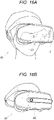
- Fig. 16A is a plan view illustrating an example in which the electronic apparatus 2 according to any of the first to seventh embodiments is applied to a head-mounted display (HMD) 61.
- the HMD 61 in Fig. 16A is used for virtual reality (VR), augmented reality (AR), mixed reality (MR), substituional reality (SR), or the like.
- the current HMD is equipped with a camera 62 on its outer front face.
- the wearer of the HMD can visually recognize the surrounding image but a person around the wearer cannot recognize the eyes or facial expression of the wearer of the HMD.
- a display face of a display device 1 is provided on the outer front face of the HMD 61, and a camera module 3 is provided opposite the display face of the display device 1.
- the facial expression of the wearer shot by the camera module 3 can be displayed on the display face of the display device 1, and the person around the wearer can grasp the facial expression and eye movement of the wearer in real time.
- the camera module 3 is provided on the rear face side of the display device 1.
- the camera can be disposed at an optimum position.
- it can prevent problems such as misalignment of the eyes of the wearer displayed on the display face.
- the electronic apparatus 2 according to any of the first to seventh embodiments can be used for various applications, and its utility value can be increased.
Landscapes
- Physics & Mathematics (AREA)
- Chemical & Material Sciences (AREA)
- Inorganic Chemistry (AREA)
- General Physics & Mathematics (AREA)
- Optics & Photonics (AREA)
- Sustainable Development (AREA)
- Life Sciences & Earth Sciences (AREA)
- Health & Medical Sciences (AREA)
- Toxicology (AREA)
- Engineering & Computer Science (AREA)
- Manufacturing & Machinery (AREA)
- Signal Processing (AREA)
- Multimedia (AREA)
- Devices For Indicating Variable Information By Combining Individual Elements (AREA)
- Electroluminescent Light Sources (AREA)
Applications Claiming Priority (2)
| Application Number | Priority Date | Filing Date | Title |
|---|---|---|---|
| JP2020022417 | 2020-02-13 | ||
| PCT/JP2021/004047 WO2021161882A1 (fr) | 2020-02-13 | 2021-02-04 | Dispositif d'affichage, appareil électronique et procédé de production de dispositif d'affichage |
Publications (3)
| Publication Number | Publication Date |
|---|---|
| EP4105694A1 true EP4105694A1 (fr) | 2022-12-21 |
| EP4105694A4 EP4105694A4 (fr) | 2023-08-16 |
| EP4105694B1 EP4105694B1 (fr) | 2025-12-31 |
Family
ID=77180857
Family Applications (1)
| Application Number | Title | Priority Date | Filing Date |
|---|---|---|---|
| EP21753084.9A Active EP4105694B1 (fr) | 2020-02-13 | 2021-02-04 | Dispositif d'affichage, appareil électronique et procédé de production de dispositif d'affichage |
Country Status (8)
| Country | Link |
|---|---|
| US (1) | US20220390657A1 (fr) |
| EP (1) | EP4105694B1 (fr) |
| JP (1) | JP7612651B2 (fr) |
| KR (1) | KR20220138049A (fr) |
| CN (2) | CN113257869B (fr) |
| DE (1) | DE112021001013T5 (fr) |
| TW (1) | TW202133456A (fr) |
| WO (1) | WO2021161882A1 (fr) |
Families Citing this family (5)
| Publication number | Priority date | Publication date | Assignee | Title |
|---|---|---|---|---|
| TW202133456A (zh) * | 2020-02-13 | 2021-09-01 | 日商索尼半導體解決方案公司 | 顯示裝置、電子機器及顯示裝置之製造方法 |
| KR102819217B1 (ko) * | 2020-11-06 | 2025-06-12 | 삼성디스플레이 주식회사 | 표시 장치 및 이의 제조 방법 |
| KR102872423B1 (ko) * | 2021-11-30 | 2025-10-17 | 엘지디스플레이 주식회사 | 전원 공급회로 및 그를 포함하는 표시장치 |
| US12469325B2 (en) * | 2022-04-27 | 2025-11-11 | Omnivision Technologies, Inc. | Fingerprint sensor with wafer-bonded microlens array |
| EP4542343A4 (fr) | 2022-12-29 | 2025-11-19 | Samsung Electronics Co Ltd | Dispositif de visiocasque comprenant un capteur de suivi oculaire et procédé de fonctionnement pour dispositif de visiocasque |
Family Cites Families (19)
| Publication number | Priority date | Publication date | Assignee | Title |
|---|---|---|---|---|
| US8947627B2 (en) | 2011-10-14 | 2015-02-03 | Apple Inc. | Electronic devices having displays with openings |
| US20140184521A1 (en) * | 2012-12-28 | 2014-07-03 | Wah Yiu Y.U. Kwong | Integrated camera lens and touch screen cover for an electronic device |
| KR20160116162A (ko) | 2015-03-26 | 2016-10-07 | 삼성디스플레이 주식회사 | 표시 장치 |
| US9864400B2 (en) * | 2015-10-30 | 2018-01-09 | Essential Products, Inc. | Camera integrated into a display |
| JP6730803B2 (ja) * | 2015-12-18 | 2020-07-29 | デクセリアルズ株式会社 | 反射防止光学体の形成方法、ディスプレイパネルおよび光学フィルム |
| KR102646280B1 (ko) * | 2016-05-27 | 2024-03-12 | 삼성디스플레이 주식회사 | 표시 장치 및 이의 제조 방법 |
| US10897148B2 (en) | 2016-09-23 | 2021-01-19 | Apple Inc. | Wireless charging mats with multi-layer transmitter coil arrangements |
| EP3982618B1 (fr) * | 2017-04-25 | 2023-03-15 | Huawei Technologies Co., Ltd. | Dispositif électronique avec écran lcd |
| KR102758516B1 (ko) * | 2018-10-05 | 2025-01-22 | 삼성디스플레이 주식회사 | 표시 장치 |
| CN109616587B (zh) * | 2018-12-04 | 2021-10-08 | 京东方科技集团股份有限公司 | 显示基板及其制造方法和显示装置 |
| CN109671858B (zh) * | 2018-12-06 | 2021-03-23 | 武汉华星光电半导体显示技术有限公司 | 一种显示屏的制作方法 |
| CN111384064B (zh) * | 2018-12-29 | 2022-05-31 | 武汉华星光电半导体显示技术有限公司 | 一种显示面板及其终端器件 |
| CN110071121B (zh) * | 2019-04-17 | 2020-09-08 | 武汉华星光电半导体显示技术有限公司 | 显示面板及显示装置 |
| CN110534541A (zh) * | 2019-08-30 | 2019-12-03 | 武汉天马微电子有限公司 | 一种电致发光显示面板及显示装置 |
| CN110581910A (zh) * | 2019-09-17 | 2019-12-17 | Oppo广东移动通信有限公司 | 图像采集方法、装置、终端及存储介质 |
| CN110783347A (zh) * | 2019-10-12 | 2020-02-11 | 武汉华星光电半导体显示技术有限公司 | 一种显示面板及其制备方法 |
| CN111312755B (zh) * | 2019-11-29 | 2021-06-08 | 昆山国显光电有限公司 | 显示面板及显示装置 |
| KR102928331B1 (ko) * | 2020-02-07 | 2026-02-19 | 삼성디스플레이 주식회사 | 표시 장치 및 전자 기기 |
| TW202133456A (zh) * | 2020-02-13 | 2021-09-01 | 日商索尼半導體解決方案公司 | 顯示裝置、電子機器及顯示裝置之製造方法 |
-
2021
- 2021-01-12 TW TW110101044A patent/TW202133456A/zh unknown
- 2021-02-04 EP EP21753084.9A patent/EP4105694B1/fr active Active
- 2021-02-04 WO PCT/JP2021/004047 patent/WO2021161882A1/fr not_active Ceased
- 2021-02-04 DE DE112021001013.1T patent/DE112021001013T5/de active Pending
- 2021-02-04 US US17/790,025 patent/US20220390657A1/en active Pending
- 2021-02-04 JP JP2022500350A patent/JP7612651B2/ja active Active
- 2021-02-04 CN CN202110155368.5A patent/CN113257869B/zh active Active
- 2021-02-04 KR KR1020227026628A patent/KR20220138049A/ko active Pending
- 2021-02-04 CN CN202120325226.4U patent/CN214477459U/zh active Active
Also Published As
| Publication number | Publication date |
|---|---|
| WO2021161882A1 (fr) | 2021-08-19 |
| KR20220138049A (ko) | 2022-10-12 |
| JP7612651B2 (ja) | 2025-01-14 |
| US20220390657A1 (en) | 2022-12-08 |
| CN113257869A (zh) | 2021-08-13 |
| CN214477459U (zh) | 2021-10-22 |
| CN113257869B (zh) | 2025-07-18 |
| TW202133456A (zh) | 2021-09-01 |
| EP4105694B1 (fr) | 2025-12-31 |
| JPWO2021161882A1 (fr) | 2021-08-19 |
| EP4105694A4 (fr) | 2023-08-16 |
| DE112021001013T5 (de) | 2023-01-26 |
Similar Documents
| Publication | Publication Date | Title |
|---|---|---|
| EP4105694A1 (fr) | Dispositif d'affichage, appareil électronique et procédé de production de dispositif d'affichage | |
| CN210349840U (zh) | 光学传感器 | |
| TWI765170B (zh) | 光學感測器、光學感測系統及其製造方法 | |
| US9977248B1 (en) | Augmented reality display system | |
| US20190057957A1 (en) | Augmented reality display system | |
| WO2019206079A1 (fr) | Panneau d'affichage et dispositif d'affichage | |
| US20250216587A1 (en) | Light emitting device, exposure system, imaging display device, imaging device, electronic device, and lighting device | |
| KR20220056788A (ko) | 발광장치, 표시장치, 촬상장치, 및 전자기기 | |
| TWM595331U (zh) | 光學感測器以及光學感測系統 | |
| CN114092980A (zh) | 指纹传感器和包括该指纹传感器的显示装置 | |
| CN212392247U (zh) | 屏内光学生物特征感测装置 | |
| JP4238356B2 (ja) | 認証システム、光放射装置、認証装置および認証方法 | |
| CN111898397B (zh) | 纹路识别装置 | |
| KR20210119007A (ko) | 표시장치 및 이의 제조 방법 | |
| US20230329036A1 (en) | Image display device and electronic device | |
| EP4383984A1 (fr) | Dispositif à semi-conducteur, dispositif d'affichage, dispositif de conversion photoélectrique, appareil électronique, dispositif d'éclairage, corps mobile, et procédé de fabrication | |
| US20230232693A1 (en) | Image display device and electronic device | |
| US20250241111A1 (en) | Light emitting device, display device, photoelectric conversion device, electronic apparatus, and wearable device | |
| CN122003025A (zh) | 显示面板和电子设备 | |
| CN117135955A (zh) | 电子装置 | |
| JP2023178185A (ja) | 電子モジュール、表示装置、光電変換装置、および、電子機器 | |
| JP2026062076A (ja) | 発光装置およびその製造方法、ならびに発光装置を含む装置 | |
| JP2025185552A (ja) | 発光デバイス、発光モジュールおよび画像形成装置 | |
| JP2024109028A (ja) | 発光装置、光電変換装置、電子機器、照明装置及び移動体 | |
| CN121712221A (zh) | 显示装置、包括多个像素的装置和摄像装置 |
Legal Events
| Date | Code | Title | Description |
|---|---|---|---|
| STAA | Information on the status of an ep patent application or granted ep patent |
Free format text: STATUS: THE INTERNATIONAL PUBLICATION HAS BEEN MADE |
|
| PUAI | Public reference made under article 153(3) epc to a published international application that has entered the european phase |
Free format text: ORIGINAL CODE: 0009012 |
|
| STAA | Information on the status of an ep patent application or granted ep patent |
Free format text: STATUS: REQUEST FOR EXAMINATION WAS MADE |
|
| 17P | Request for examination filed |
Effective date: 20220727 |
|
| AK | Designated contracting states |
Kind code of ref document: A1 Designated state(s): AL AT BE BG CH CY CZ DE DK EE ES FI FR GB GR HR HU IE IS IT LI LT LU LV MC MK MT NL NO PL PT RO RS SE SI SK SM TR |
|
| DAV | Request for validation of the european patent (deleted) | ||
| DAX | Request for extension of the european patent (deleted) | ||
| A4 | Supplementary search report drawn up and despatched |
Effective date: 20230714 |
|
| RIC1 | Information provided on ipc code assigned before grant |
Ipc: G02B 27/01 20060101ALI20230710BHEP Ipc: G02B 1/118 20150101ALI20230710BHEP Ipc: H05B 33/10 20060101ALI20230710BHEP Ipc: H05B 33/04 20060101ALI20230710BHEP Ipc: H05B 33/02 20060101ALI20230710BHEP Ipc: H01L 27/146 20060101ALI20230710BHEP Ipc: G09F 9/30 20060101ALI20230710BHEP Ipc: G09F 9/00 20060101ALI20230710BHEP Ipc: G02B 5/02 20060101AFI20230710BHEP |
|
| STAA | Information on the status of an ep patent application or granted ep patent |
Free format text: STATUS: EXAMINATION IS IN PROGRESS |
|
| RIC1 | Information provided on ipc code assigned before grant |
Ipc: G02B 5/20 20060101ALI20240927BHEP Ipc: G09F 9/00 20060101ALI20240927BHEP Ipc: G09F 9/30 20060101ALI20240927BHEP Ipc: H01L 27/146 20060101ALI20240927BHEP Ipc: H05B 33/02 20060101ALI20240927BHEP Ipc: H05B 33/04 20060101ALI20240927BHEP Ipc: H05B 33/10 20060101ALI20240927BHEP Ipc: G02B 1/118 20150101ALI20240927BHEP Ipc: G02B 27/01 20060101ALI20240927BHEP Ipc: G02B 5/02 20060101AFI20240927BHEP |
|
| 17Q | First examination report despatched |
Effective date: 20241024 |
|
| RIC1 | Information provided on ipc code assigned before grant |
Ipc: G02B 5/02 20060101AFI20250911BHEP Ipc: H05B 33/02 20060101ALI20250911BHEP Ipc: H05B 33/04 20060101ALI20250911BHEP Ipc: H05B 33/10 20060101ALI20250911BHEP Ipc: G02B 1/118 20150101ALI20250911BHEP Ipc: G02B 27/01 20060101ALI20250911BHEP Ipc: G09F 9/30 20060101ALI20250911BHEP |
|
| GRAP | Despatch of communication of intention to grant a patent |
Free format text: ORIGINAL CODE: EPIDOSNIGR1 |
|
| STAA | Information on the status of an ep patent application or granted ep patent |
Free format text: STATUS: GRANT OF PATENT IS INTENDED |
|
| INTG | Intention to grant announced |
Effective date: 20251017 |
|
| GRAS | Grant fee paid |
Free format text: ORIGINAL CODE: EPIDOSNIGR3 |
|
| GRAA | (expected) grant |
Free format text: ORIGINAL CODE: 0009210 |
|
| STAA | Information on the status of an ep patent application or granted ep patent |
Free format text: STATUS: THE PATENT HAS BEEN GRANTED |
|
| P01 | Opt-out of the competence of the unified patent court (upc) registered |
Free format text: CASE NUMBER: UPC_APP_0013258_4105694/2025 Effective date: 20251113 |
|
| AK | Designated contracting states |
Kind code of ref document: B1 Designated state(s): AL AT BE BG CH CY CZ DE DK EE ES FI FR GB GR HR HU IE IS IT LI LT LU LV MC MK MT NL NO PL PT RO RS SE SI SK SM TR |
|
| REG | Reference to a national code |
Ref country code: CH Ref legal event code: F10 Free format text: ST27 STATUS EVENT CODE: U-0-0-F10-F00 (AS PROVIDED BY THE NATIONAL OFFICE) Effective date: 20251231 Ref country code: GB Ref legal event code: FG4D |
|
| REG | Reference to a national code |
Ref country code: DE Ref legal event code: R096 Ref document number: 602021045473 Country of ref document: DE |
|
| REG | Reference to a national code |
Ref country code: IE Ref legal event code: FG4D |
|
| PGFP | Annual fee paid to national office [announced via postgrant information from national office to epo] |
Ref country code: NL Payment date: 20260121 Year of fee payment: 6 |
|
| REG | Reference to a national code |
Ref country code: NL Ref legal event code: FP |
|
| PGFP | Annual fee paid to national office [announced via postgrant information from national office to epo] |
Ref country code: GB Payment date: 20260122 Year of fee payment: 6 |
|
| REG | Reference to a national code |
Ref country code: LT Ref legal event code: MG9D |
|
| PG25 | Lapsed in a contracting state [announced via postgrant information from national office to epo] |
Ref country code: NO Free format text: LAPSE BECAUSE OF FAILURE TO SUBMIT A TRANSLATION OF THE DESCRIPTION OR TO PAY THE FEE WITHIN THE PRESCRIBED TIME-LIMIT Effective date: 20260331 |
|
| PGFP | Annual fee paid to national office [announced via postgrant information from national office to epo] |
Ref country code: DE Payment date: 20260121 Year of fee payment: 6 |
|
| PG25 | Lapsed in a contracting state [announced via postgrant information from national office to epo] |
Ref country code: FI Free format text: LAPSE BECAUSE OF FAILURE TO SUBMIT A TRANSLATION OF THE DESCRIPTION OR TO PAY THE FEE WITHIN THE PRESCRIBED TIME-LIMIT Effective date: 20251231 Ref country code: HR Free format text: LAPSE BECAUSE OF FAILURE TO SUBMIT A TRANSLATION OF THE DESCRIPTION OR TO PAY THE FEE WITHIN THE PRESCRIBED TIME-LIMIT Effective date: 20251231 |
|
| PG25 | Lapsed in a contracting state [announced via postgrant information from national office to epo] |
Ref country code: RS Free format text: LAPSE BECAUSE OF FAILURE TO SUBMIT A TRANSLATION OF THE DESCRIPTION OR TO PAY THE FEE WITHIN THE PRESCRIBED TIME-LIMIT Effective date: 20260331 |
|
| PGFP | Annual fee paid to national office [announced via postgrant information from national office to epo] |
Ref country code: FR Payment date: 20260121 Year of fee payment: 6 |
|
| PG25 | Lapsed in a contracting state [announced via postgrant information from national office to epo] |
Ref country code: LV Free format text: LAPSE BECAUSE OF FAILURE TO SUBMIT A TRANSLATION OF THE DESCRIPTION OR TO PAY THE FEE WITHIN THE PRESCRIBED TIME-LIMIT Effective date: 20251231 |