EP4109340A1 - Étiquettes rfid dotées d'une structure de blindage destinées à être incorporées dans un emballage alimentaire allant au four à micro-ondes - Google Patents
Étiquettes rfid dotées d'une structure de blindage destinées à être incorporées dans un emballage alimentaire allant au four à micro-ondes Download PDFInfo
- Publication number
- EP4109340A1 EP4109340A1 EP22189193.0A EP22189193A EP4109340A1 EP 4109340 A1 EP4109340 A1 EP 4109340A1 EP 22189193 A EP22189193 A EP 22189193A EP 4109340 A1 EP4109340 A1 EP 4109340A1
- Authority
- EP
- European Patent Office
- Prior art keywords
- antenna
- rfid tag
- conductor
- rfid
- gap
- Prior art date
- Legal status (The legal status is an assumption and is not a legal conclusion. Google has not performed a legal analysis and makes no representation as to the accuracy of the status listed.)
- Granted
Links
Images


Classifications
-
- G—PHYSICS
- G06—COMPUTING OR CALCULATING; COUNTING
- G06K—GRAPHICAL DATA READING; PRESENTATION OF DATA; RECORD CARRIERS; HANDLING RECORD CARRIERS
- G06K19/00—Record carriers for use with machines and with at least a part designed to carry digital markings
- G06K19/06—Record carriers for use with machines and with at least a part designed to carry digital markings characterised by the kind of the digital marking, e.g. shape, nature, code
- G06K19/067—Record carriers with conductive marks, printed circuits or semiconductor circuit elements, e.g. credit or identity cards also with resonating or responding marks without active components
- G06K19/07—Record carriers with conductive marks, printed circuits or semiconductor circuit elements, e.g. credit or identity cards also with resonating or responding marks without active components with integrated circuit chips
- G06K19/077—Constructional details, e.g. mounting of circuits in the carrier
- G06K19/0772—Physical layout of the record carrier
- G06K19/0773—Physical layout of the record carrier the record carrier comprising means to protect itself against external heat sources
-
- G—PHYSICS
- G06—COMPUTING OR CALCULATING; COUNTING
- G06K—GRAPHICAL DATA READING; PRESENTATION OF DATA; RECORD CARRIERS; HANDLING RECORD CARRIERS
- G06K19/00—Record carriers for use with machines and with at least a part designed to carry digital markings
- G06K19/06—Record carriers for use with machines and with at least a part designed to carry digital markings characterised by the kind of the digital marking, e.g. shape, nature, code
- G06K19/067—Record carriers with conductive marks, printed circuits or semiconductor circuit elements, e.g. credit or identity cards also with resonating or responding marks without active components
- G06K19/07—Record carriers with conductive marks, printed circuits or semiconductor circuit elements, e.g. credit or identity cards also with resonating or responding marks without active components with integrated circuit chips
- G06K19/077—Constructional details, e.g. mounting of circuits in the carrier
- G06K19/07749—Constructional details, e.g. mounting of circuits in the carrier the record carrier being capable of non-contact communication, e.g. constructional details of the antenna of a non-contact smart card
- G06K19/07773—Antenna details
-
- B—PERFORMING OPERATIONS; TRANSPORTING
- B65—CONVEYING; PACKING; STORING; HANDLING THIN OR FILAMENTARY MATERIAL
- B65D—CONTAINERS FOR STORAGE OR TRANSPORT OF ARTICLES OR MATERIALS, e.g. BAGS, BARRELS, BOTTLES, BOXES, CANS, CARTONS, CRATES, DRUMS, JARS, TANKS, HOPPERS, FORWARDING CONTAINERS; ACCESSORIES, CLOSURES, OR FITTINGS THEREFOR; PACKAGING ELEMENTS; PACKAGES
- B65D81/00—Containers, packaging elements, or packages, for contents presenting particular transport or storage problems, or adapted to be used for non-packaging purposes after removal of contents
- B65D81/34—Containers, packaging elements, or packages, for contents presenting particular transport or storage problems, or adapted to be used for non-packaging purposes after removal of contents for packaging foodstuffs or other articles intended to be cooked or heated within the package
- B65D81/3446—Containers, packaging elements, or packages, for contents presenting particular transport or storage problems, or adapted to be used for non-packaging purposes after removal of contents for packaging foodstuffs or other articles intended to be cooked or heated within the package specially adapted to be heated by microwaves
- B65D81/3453—Rigid containers, e.g. trays, bottles, boxes, cups
-
- G—PHYSICS
- G06—COMPUTING OR CALCULATING; COUNTING
- G06K—GRAPHICAL DATA READING; PRESENTATION OF DATA; RECORD CARRIERS; HANDLING RECORD CARRIERS
- G06K19/00—Record carriers for use with machines and with at least a part designed to carry digital markings
- G06K19/06—Record carriers for use with machines and with at least a part designed to carry digital markings characterised by the kind of the digital marking, e.g. shape, nature, code
- G06K19/067—Record carriers with conductive marks, printed circuits or semiconductor circuit elements, e.g. credit or identity cards also with resonating or responding marks without active components
- G06K19/07—Record carriers with conductive marks, printed circuits or semiconductor circuit elements, e.g. credit or identity cards also with resonating or responding marks without active components with integrated circuit chips
- G06K19/0701—Record carriers with conductive marks, printed circuits or semiconductor circuit elements, e.g. credit or identity cards also with resonating or responding marks without active components with integrated circuit chips at least one of the integrated circuit chips comprising an arrangement for power management
- G06K19/0715—Record carriers with conductive marks, printed circuits or semiconductor circuit elements, e.g. credit or identity cards also with resonating or responding marks without active components with integrated circuit chips at least one of the integrated circuit chips comprising an arrangement for power management the arrangement including means to regulate power transfer to the integrated circuit
-
- G—PHYSICS
- G06—COMPUTING OR CALCULATING; COUNTING
- G06K—GRAPHICAL DATA READING; PRESENTATION OF DATA; RECORD CARRIERS; HANDLING RECORD CARRIERS
- G06K19/00—Record carriers for use with machines and with at least a part designed to carry digital markings
- G06K19/06—Record carriers for use with machines and with at least a part designed to carry digital markings characterised by the kind of the digital marking, e.g. shape, nature, code
- G06K19/067—Record carriers with conductive marks, printed circuits or semiconductor circuit elements, e.g. credit or identity cards also with resonating or responding marks without active components
- G06K19/07—Record carriers with conductive marks, printed circuits or semiconductor circuit elements, e.g. credit or identity cards also with resonating or responding marks without active components with integrated circuit chips
- G06K19/0723—Record carriers with conductive marks, printed circuits or semiconductor circuit elements, e.g. credit or identity cards also with resonating or responding marks without active components with integrated circuit chips the record carrier comprising an arrangement for non-contact communication, e.g. wireless communication circuits on transponder cards, non-contact smart cards or RFIDs
-
- G—PHYSICS
- G06—COMPUTING OR CALCULATING; COUNTING
- G06K—GRAPHICAL DATA READING; PRESENTATION OF DATA; RECORD CARRIERS; HANDLING RECORD CARRIERS
- G06K19/00—Record carriers for use with machines and with at least a part designed to carry digital markings
- G06K19/06—Record carriers for use with machines and with at least a part designed to carry digital markings characterised by the kind of the digital marking, e.g. shape, nature, code
- G06K19/067—Record carriers with conductive marks, printed circuits or semiconductor circuit elements, e.g. credit or identity cards also with resonating or responding marks without active components
- G06K19/07—Record carriers with conductive marks, printed circuits or semiconductor circuit elements, e.g. credit or identity cards also with resonating or responding marks without active components with integrated circuit chips
- G06K19/077—Constructional details, e.g. mounting of circuits in the carrier
- G06K19/07749—Constructional details, e.g. mounting of circuits in the carrier the record carrier being capable of non-contact communication, e.g. constructional details of the antenna of a non-contact smart card
- G06K19/0775—Constructional details, e.g. mounting of circuits in the carrier the record carrier being capable of non-contact communication, e.g. constructional details of the antenna of a non-contact smart card arrangements for connecting the integrated circuit to the antenna
- G06K19/07752—Constructional details, e.g. mounting of circuits in the carrier the record carrier being capable of non-contact communication, e.g. constructional details of the antenna of a non-contact smart card arrangements for connecting the integrated circuit to the antenna using an interposer
-
- G—PHYSICS
- G06—COMPUTING OR CALCULATING; COUNTING
- G06K—GRAPHICAL DATA READING; PRESENTATION OF DATA; RECORD CARRIERS; HANDLING RECORD CARRIERS
- G06K19/00—Record carriers for use with machines and with at least a part designed to carry digital markings
- G06K19/06—Record carriers for use with machines and with at least a part designed to carry digital markings characterised by the kind of the digital marking, e.g. shape, nature, code
- G06K19/067—Record carriers with conductive marks, printed circuits or semiconductor circuit elements, e.g. credit or identity cards also with resonating or responding marks without active components
- G06K19/07—Record carriers with conductive marks, printed circuits or semiconductor circuit elements, e.g. credit or identity cards also with resonating or responding marks without active components with integrated circuit chips
- G06K19/077—Constructional details, e.g. mounting of circuits in the carrier
- G06K19/07749—Constructional details, e.g. mounting of circuits in the carrier the record carrier being capable of non-contact communication, e.g. constructional details of the antenna of a non-contact smart card
- G06K19/07771—Constructional details, e.g. mounting of circuits in the carrier the record carrier being capable of non-contact communication, e.g. constructional details of the antenna of a non-contact smart card the record carrier comprising means for minimising adverse effects on the data communication capability of the record carrier, e.g. minimising Eddy currents induced in a proximate metal or otherwise electromagnetically interfering object
-
- G—PHYSICS
- G06—COMPUTING OR CALCULATING; COUNTING
- G06K—GRAPHICAL DATA READING; PRESENTATION OF DATA; RECORD CARRIERS; HANDLING RECORD CARRIERS
- G06K19/00—Record carriers for use with machines and with at least a part designed to carry digital markings
- G06K19/06—Record carriers for use with machines and with at least a part designed to carry digital markings characterised by the kind of the digital marking, e.g. shape, nature, code
- G06K19/067—Record carriers with conductive marks, printed circuits or semiconductor circuit elements, e.g. credit or identity cards also with resonating or responding marks without active components
- G06K19/07—Record carriers with conductive marks, printed circuits or semiconductor circuit elements, e.g. credit or identity cards also with resonating or responding marks without active components with integrated circuit chips
- G06K19/077—Constructional details, e.g. mounting of circuits in the carrier
- G06K19/07749—Constructional details, e.g. mounting of circuits in the carrier the record carrier being capable of non-contact communication, e.g. constructional details of the antenna of a non-contact smart card
- G06K19/07773—Antenna details
- G06K19/07775—Antenna details the antenna being on-chip
-
- G—PHYSICS
- G06—COMPUTING OR CALCULATING; COUNTING
- G06K—GRAPHICAL DATA READING; PRESENTATION OF DATA; RECORD CARRIERS; HANDLING RECORD CARRIERS
- G06K19/00—Record carriers for use with machines and with at least a part designed to carry digital markings
- G06K19/06—Record carriers for use with machines and with at least a part designed to carry digital markings characterised by the kind of the digital marking, e.g. shape, nature, code
- G06K19/067—Record carriers with conductive marks, printed circuits or semiconductor circuit elements, e.g. credit or identity cards also with resonating or responding marks without active components
- G06K19/07—Record carriers with conductive marks, printed circuits or semiconductor circuit elements, e.g. credit or identity cards also with resonating or responding marks without active components with integrated circuit chips
- G06K19/077—Constructional details, e.g. mounting of circuits in the carrier
- G06K19/07749—Constructional details, e.g. mounting of circuits in the carrier the record carrier being capable of non-contact communication, e.g. constructional details of the antenna of a non-contact smart card
- G06K19/07773—Antenna details
- G06K19/07786—Antenna details the antenna being of the HF type, such as a dipole
-
- G—PHYSICS
- G06—COMPUTING OR CALCULATING; COUNTING
- G06K—GRAPHICAL DATA READING; PRESENTATION OF DATA; RECORD CARRIERS; HANDLING RECORD CARRIERS
- G06K19/00—Record carriers for use with machines and with at least a part designed to carry digital markings
- G06K19/06—Record carriers for use with machines and with at least a part designed to carry digital markings characterised by the kind of the digital marking, e.g. shape, nature, code
- G06K19/067—Record carriers with conductive marks, printed circuits or semiconductor circuit elements, e.g. credit or identity cards also with resonating or responding marks without active components
- G06K19/07—Record carriers with conductive marks, printed circuits or semiconductor circuit elements, e.g. credit or identity cards also with resonating or responding marks without active components with integrated circuit chips
- G06K19/077—Constructional details, e.g. mounting of circuits in the carrier
- G06K19/07749—Constructional details, e.g. mounting of circuits in the carrier the record carrier being capable of non-contact communication, e.g. constructional details of the antenna of a non-contact smart card
- G06K19/07798—Constructional details, e.g. mounting of circuits in the carrier the record carrier being capable of non-contact communication, e.g. constructional details of the antenna of a non-contact smart card part of the antenna or the integrated circuit being adapted for rupturing or breaking, e.g. record carriers functioning as sealing devices for detecting not-authenticated opening of containers
-
- B—PERFORMING OPERATIONS; TRANSPORTING
- B65—CONVEYING; PACKING; STORING; HANDLING THIN OR FILAMENTARY MATERIAL
- B65D—CONTAINERS FOR STORAGE OR TRANSPORT OF ARTICLES OR MATERIALS, e.g. BAGS, BARRELS, BOTTLES, BOXES, CANS, CARTONS, CRATES, DRUMS, JARS, TANKS, HOPPERS, FORWARDING CONTAINERS; ACCESSORIES, CLOSURES, OR FITTINGS THEREFOR; PACKAGING ELEMENTS; PACKAGES
- B65D2203/00—Decoration means, markings, information elements, contents indicators
- B65D2203/10—Transponders
Definitions
- the present subject matter relates to packaging for microwavable food items. More particularly, the present subject matter relates to radio frequency identification (“RFID”) tags incorporated into packaging for microwavable food items.
- RFID radio frequency identification
- crisping sleeves are paper items that at least partially surround the food item during microwaving.
- a "crisping sleeve” has a paper substrate, with a susceptor incorporated into the inner surface of the "crisping sleeve,” facing and preferably in contact with the food item.
- the susceptor which may be a metallized film, absorbs microwave energy and converts it into heat, which crisps and/or browns the crust or surface of the food item, thus improving the look and texture of the food item. Due to the absorbing nature of the film used as the susceptor, relatively low levels of energy are reflected by it, such that it does not strike an arc due to generating high differential voltages between adjacent parts of the film, which could otherwise cause the packaging to catch fire.
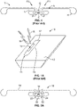
- Fig. 1 shows an RFID tag T according to conventional design, which may be secured to or otherwise associated with an enclosure like that of enclosure 13 of Fig. 1A (typically, a paper or cardboard sleeve or box) of the package 9 for a microwavable food item in respect to Fig. 1A .
- the entirety of the packaging 9 of Fig. 1A is not intended to be microwaved, but rather the food item (and, optionally, a "crisping sleeve” or the like) is removed from the enclosure 13 of Fig. 1A and inserted into the microwave oven for heating/cooking.
- the RFID tag T of Fig. 1 includes an RFID chip C, with an associated dipole antenna A for transmitting information to and/or receiving information from an RFID reader (not illustrated).
- the RFID chip C is electrically coupled to the antenna A across a gap G defined by the antenna A between two conductor pad areas P.
- RFID tags inherently must, at some point, have a gap across which the RFID chip is placed that has a voltage at the intended frequency of operation when in the field of a reader device.
- the power required incident on the RFID chip C may be as low as 10 microwatts, whereas a microwave oven may typically operate at a power level in excess of 800 watts, which can generate very high voltages across the gap G and the associated RFID chip C.
- the antenna A is designed to operate at a first frequency F1, for example in the range of approximately 860 MHz to 930 MHz, with the antenna A taking incident power at the first frequency F1 from an RFID reader and converting it to a voltage across the RFID chip C to allow it to operate.
- the antenna A is not designed to operate at the second frequency F2, as the very high power levels incident at second frequency F2 will generate high voltages on the antenna A. These high voltages can appear at a number of places on the antenna A; however, by methods such as introducing large gaps L between antenna elements and controlled radii (identified generally at R in Fig. 1 ), a voltage across said elements that would generate a high voltage breakdown and, hence, arc can be avoided.
- the gap G bridged by the RFID chip C is necessarily relatively small and, hence, a high voltage arises at the second frequency F2, which high voltage may cause a breakdown and generate an arc.
- the dipole antenna 17 can receive microwave energy (identified in Fig. 1A at M) and reflect the microwave energy (represented in Fig. 1A at R) into the microwave source.
- an arc may be created between adjacent sections of the dipole antenna 17 (which location may be between the two conductive elements of the dipole antenna 17, as identified in Fig. 1A at 19).
- the dipole antenna 17 of the conventional RFID tag 11 is formed of relatively thick, low resistance conductor, which has different properties than the metallic film used to define a typical susceptor.
- common susceptors are made from metal-coated films with optical densities ranging from 0.18 to 0.29, corresponding to a sheet resistance of 100 ohms to 230 ohms, whereas a material of less than 1 ohm per square is commonly used to form the antenna 18 of the RFID tag 11.
- the RFID tag 11 can cause issues if it is not dissociated from the food item prior to microwaving the food item (i.e., if the entire package 9 of Fig. 1A is placed into the microwave oven).
- the RFID tag T and 11 of Fig. 1 and 1A respectively are typically configured to be readily removable or otherwise dissociable from the food item, such as by securing it to the enclosure of the package, which may include instructions to not microwave the enclosure.
- a user failing to take proper care could place the entire package (including the RFID tag T and 11 shown in Fig. 1 and 1A respectively) into the microwave oven with the food item, thereby failing to dissociate the RFID tag T or 11 from the food item.
- an RFID tag in one aspect, includes an antenna defining a gap and configured to operate at a first frequency.
- An RFID chip and an antenna electrically coupled to the antenna across the gap.
- a shielding structure is electrically coupled to the antenna across the gap and overlays the RFID chip.
- the shielding structure includes a shield conductor and a shield dielectric at least partially positioned between the shield conductor and the RFID chip. The shielding structure is configured to limit the voltage across the gap when the antenna is exposed to a second frequency that is greater than the first frequency.
- packaging for a microwavable food item.
- the packaging includes an enclosure and an RFID tag secured to the enclosure.
- the RFID tag includes an antenna defining a gap and configured to operate at a first frequency.
- An RFID chip is electrically coupled to the antenna across the gap.
- a shielding structure is electrically coupled to the antenna across the gap and overlays the RFID chip.
- the shielding structure includes a shield conductor and a shield dielectric at least partially positioned between the shield conductor and the RFID chip. The shielding structure is configured to limit the voltage across the gap when the antenna is exposed to a second frequency that is greater than the first frequency.
- an RFID tag in a further aspect, includes an antenna defining a gap and configured to operate at a first frequency.
- An RFID chip is electrically coupled to the antenna across the gap.
- a shielding structure is electrically coupled to the antenna across the gap and overlays the RFID chip.
- the shielding structure includes a shield conductor and a shield dielectric at least partially positioned between the shield conductor and the RFID chip.
- a second shielding structure is electrically coupled to the antenna across the gap, underlying the RFID chip. The shielding structure is configured to limit the voltage across the gap when the antenna is exposed to a second frequency that is greater than the first frequency.
- packaging for a microwavable food item.
- the packaging includes an enclosure and an RFID tag secured to the enclosure.
- the RFID tag includes an antenna defining a gap and configured to operate at a first frequency.
- An RFID chip is electrically coupled to the antenna across the gap.
- a shielding structure is electrically coupled to the antenna across the gap and overlays the RFID chip.
- the shielding structure includes a shield conductor and a shield dielectric at least partially positioned between the shield conductor and the RFID chip.
- a second shielding structure is electrically coupled to the antenna across the gap, underlying the RFID chip. The shielding structure is configured to limit the voltage across the gap when the antenna is exposed to a second frequency that is greater than the first frequency.
- an RFID tag in another aspect, includes an RFID chip and an antenna electrically coupled to the RFID chip.
- the antenna is comprised of a conductor formed of a base material and a second material with different coefficients of thermal expansion configured to cause the antenna to fracture into multiple pieces upon being subjected to heating.
- a package for a microwavable food item.
- the package includes an enclosure, an RFID label, and a joinder material sandwiched between the RFID label and the enclosure.
- the RFID label includes a substrate and an RFID tag associated with the substrate.
- the RFID tag includes an RFID chip and an antenna electrically coupled to the RFID chip.
- the joinder material has a greater resistance than the antenna.
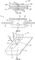
- Figs. 2A and 2B show an RFID tag 10 according to the present disclosure
- Fig. 2B shows the RFID tag, generally designated at 10, secured to the enclosure 12 (e.g., a paper box) of packaging, generally designated at 14, for a microwavable food item.
- the packaging 14 may include other items, such as a "crisping sleeve" configured to be microwaved with the food item.
- the RFID tag 10 may be incorporated into the packaging 14 by any suitable approach and, while the RFID tag 10 is secured to the enclosure 12 in the embodiment of Fig. 2B , the RFID tag 10 may be associated with another portion of the packaging 14 (e.g., a "crisping sleeve" housed within the enclosure 12) in other embodiments.
- RFID tags are described herein as being incorporated into the packaging of a microwavable food item, it should be understood that RFID tags according to the present disclosure may be useful in any of a number of possible applications, particularly when it is contemplated that they may be exposed to frequencies (referred to herein as a "second frequency") that are significantly higher than the frequency (referred to herein as a "first frequency”) at which an antenna of the RFID tag is intended to operate.
- a second frequency frequencies
- first frequency the frequency at which an antenna of the RFID tag is intended to operate.
- the RFID tag 10 includes an antenna 16 with an RFID chip 18 electrically coupled thereto.
- the antenna 16 is provided as a dipole antenna, which is formed of a conductor defining a gap 20 between two conductor pad areas 22 ( Fig. 2A ), which is bridged by the RFID chip 18.
- the antenna 16 and RFID chip 18 may be provided generally according to conventional design (e.g., as described above with respect to the embodiment of Fig. 1 ), with the antenna 16 being designed to operate at a first frequency, which may be in the range of approximately 860 MHz to 930 MHz.
- the antenna 16 takes incident power at the first frequency and converts it to a voltage across the RFID chip 18 to allow it to operate.
- the RFID chip 18 may take any of a number of forms (including those of the type commonly referred to as a "chip” or a “strap" by one of ordinary skill in the art), including any of a number of possible components and being configured to perform any of a number of possible functions.
- the RFID chip 18 includes an integrated circuit for controlling RF communication and other functions of the RFID tag 10.
- the RFID tag 10 further includes a shielding structure, generally designated at 24, which is comprised of a shield conductor 26 and a shield dielectric 28.
- the shield conductor 26 is formed of a material having conductive properties and, as will be described in greater detail, may be variously configured without departing from the scope of the present disclosure.
- the shield dielectric 28 is formed of a material having dielectric properties and, as will be described in greater detail, may be variously configured without departing from the scope of the present disclosure.
- the shield conductor 26 and shield dielectric 28 are generally flat or planar, substantially identically shaped, and oriented with the perimeter of the shield conductor 26 coinciding with the perimeter of the shield dielectric 28.
- the shield conductor and shield dielectric may be differently configured and/or oriented at least partially out of alignment (i.e., with a portion of the shield conductor extending beyond the perimeter of the shield dielectric and/or a portion of the shield dielectric extending beyond the perimeter of the shield conductor).
- the shielding structure 24 is electrically coupled to the antenna 16 across the gap 20, being coupled by capacitance to the conductor pad areas 22 on either side of the gap 20 ( Fig. 2A ). As shown in Fig. 2B , the shielding structure 24 overlays the RFID chip 18, with the shield dielectric 28 at least partially positioned between the RFID chip 18 and the shield conductor 26. The shielding structure 24 may overlay or cover all (as in Figs. 2A and 2B ) or only a portion of the gap 20.
- the RFID tag 10 it is possible for the RFID tag 10 to be exposed to signals operating at first or second frequencies.
- the shielding structure 24 forms a partial short circuit across the gap 20.
- the antenna 16 is configured so as to compensate for the presence of the partial short circuit, thereby allowing the RFID tag 10 to operate properly.
- the RFID tag 10 may be placed into a microwave and exposed to the attendant high-frequency signals (which may be on the order of approximately 2,450 MHz) without the risk of ignition, unlike a conventional RFID tag T.
- Figs. 3A and 3B show an embodiment of an RFID tag, generally designated at 10a, (and associated packaging, generally designated at 14a, in Fig. 3B ) in which the shielding structure 24a includes a differently configured shield dielectric 28a ( Fig. 3B ).
- the shield dielectric 28a is incorporated into an over-lamination layer, which overlays the RFID chip 18, at least a portion of the gap 20, and at least a portion of the conductor pad areas 22 of the antenna 16 ( Fig. 3A ).
- the shield conductor 26a may comprise a patterned conductor to provide the desired bridging and shielding effects. As best seen in Fig. 3B , the shield conductor 26a and shield dielectric 28a may be differently sized and shaped, with the shield conductor 26a being smaller than the over-lamination layer into which the shield dielectric 28a is incorporated.
- Figs. 4A and 4B illustrate another embodiment of an RFID tag, generally designated at 10b, according to the present disclosure.
- the shielding structure generally designated at 24b
- the shielding structure 24b is incorporated into an RFID strap comprised of a strap conductor 30 and strap substrate 32 (along with the RFID chip 18), which is electrically coupled to the antenna 16, across the gap 20.
- the shielding structure 24b may be comprised of a shield conductor 26b applied to the strap substrate 32, which serves as the shield dielectric 28b.
- the strap substrate 32 (and any of the other shield dielectrics described herein) may be formed of any of a variety of materials, such as polyethylene terephthalate.
- Fig. 5 illustrates another embodiment of an RFID tag, generally designated at 10c, with a differently configured shielding structure 24c.
- the shield conductor 26c includes an extended area 34, which may increase the size of the shield conductor 26c beyond that of the associated shield dielectric (which is not visible in Fig. 5 ).
- the extended area 34 of the shield conductor 26c is oriented so as not to overlay the gap 20 (or the antenna 16), but rather is positioned laterally of the antenna 16 and the gap 20, extending away from the antenna 16.
- the extended area 34 of the shield conductor 26c may be variously sized and configured without departing from the scope of the present disclosure, being approximately the same size as the shield conductor 26 of Figs. 2A and 2B in one embodiment, larger than the shield conductor 26 of Figs. 2A and 2B in another embodiment, and smaller than the shield conductor 26 of Figs. 2A and 2B in yet another embodiment.
- the extended area 34 assists in dissipating heat generated across the gap 20. This effect is enhanced by increasing the size of the extended area 34, so it may be advantageous for the extended area 34 to be relatively large for improved heat dissipation.
- the extended area 34 (along with the remainder of the shield conductor 26c, as well as any of the other shield conductors described herein) may be formed of a non-flammable material, such as but not limited to, an aluminum material, heat resistant, flame resistant paper (Flex Dura HR, http://www.flexlinkllc.com/heat-resistant-paper.html), and non-flammable adhesive (Eclectic E6000 Adhesive, http://eclecticproducts.com/products/e6000.html) to provide a barrier to any arc that may be generated across the gap 20 to prevent a fire from spreading.
- a non-flammable material such as but not limited to, an aluminum material, heat resistant, flame resistant paper (Flex Dura HR, http://www.flexlinkllc.com/heat-resistant-paper.html), and non-flammable adhesive (Eclectic E6000 Adhesive, http://eclecticproducts.com/products/e6000.html) to provide a barrier to any arc that may
- Figs. 6A and 6B illustrate yet another embodiment of an RFID tag, generally designated at 10d, (and associated packaging, generally designated at 14d, in Fig. 6B ) with a differently configured shielding structure 24d.
- the shield dielectric 28d is formed of a material which undergoes reversible or non-reversible dielectric breakdown at high voltages of the type induced by a high-power microwave field.
- the shield conductor 26d may be formed by printing a conductive material (which becomes and defines the shield conductor 26d) onto the shield dielectric 28d, such as an over-lamination.
- a single RFID tag may include more than one shielding structure, as shown in the embodiment of Figs. 7A and 7B .
- the RFID tag generally designated at 10e
- a first shielding structure generally designated at 24e
- a second shielding structure generally designated at 24f
- the second shielding structure 24f underlying the RFID chip 18 (i.e., with the shielding structures 24e and 24f electrically coupled to opposing faces of the antenna 16).
- the shield dielectric 28f of the second shielding structure 24f contacts the underside of the antenna 16, while the associated shield conductor 26f is free to be secured or otherwise associated to the enclosure of a package for microwavable food or the like.
- the second shielding structure 24f is substantially identical to the first shielding structure 24e, but it is within the scope of the present disclosure for the shield conductor 26f and/or the shield dielectric 28f of the second shielding structure 24f to be differently configured from the shield conductor 26e and shield dielectric 28e of the first shielding structure 24e. Regardless of the particular configurations of the two shielding structures 24e and 24f, by providing them on both faces of the antenna 16, additional shielding is provided. This additional shielding involves additional "shorting," as there are now two partial short circuits across the gap 20. However, in accordance with the preceding description of the embodiment of Figs. 2A and 2B , the antenna 16 is configured so as to compensate for the presence of the partial short circuits, thereby allowing the RFID tag 10e to operate properly when exposed to the first frequency.
- Fig. 8 is a basic equivalent circuit representing the basic components of an RFID tag 10 according to the present disclosure.
- the gap 20 defined by the antenna 16 is bridged by an RFID chip 18 (represented by a resistor R P and a capacitor C P ) and a shielding structure 24 comprising a shield conductor 26 and a shield dielectric 28 (represented by two identical capacitors CB in series).
- the total capacitance of the shield dielectric 28 is half of the capacitance of the individual capacitors C B used to represent the shield dielectric 28 in Fig. 8 . This is calculated using the standard formula in which the total capacitance of a series of capacitors is the inverse of the sum of all inverse capacitances.
- the impedance of the shield dielectric 28 is equal to the inverse of the product of 2 ⁇ ⁇ ⁇ F ⁇ total capacitance, in which F is the frequency at which the RFID tag 10 is powered.
- F the frequency at which the RFID tag 10 is powered.
- an arc may be created between adjacent sections namely gap G and associated RFID chip C. This is in part due to adjacent sections being surrounded by a material (i.e. air or other elements) having a dielectric strength lower than that of the electric field achieved by said differential voltages across said adjacent sections. Also an arc may be created and exacerbated in part due to materials surrounding said sections that reach a temperature, due to RF current flowing along/through said adjacent sections gap G and chip C, that lowers dielectric strength of the surrounding material as well as creates flammable/combustible volatiles.
- a material i.e. air or other elements
- This arc can be avoided without the use of a shield by surrounding said sections with a material having the properties such as; a dielectric strength that can withstand the electric field at said sections, along with having heat resistant, flame resistant and non-flammable properties i.e. heat resistant and flame resistant paper and non-flammable adhesive(s).
- a material having the properties such as; a dielectric strength that can withstand the electric field at said sections, along with having heat resistant, flame resistant and non-flammable properties i.e. heat resistant and flame resistant paper and non-flammable adhesive(s).
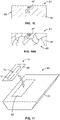
- the enclosure 23 is associated with the RFID tag 25 includes an RFID chip 27 with an antenna 29 electrically coupled thereto.
- the antenna 29 is formed of a conductor 31 having a resistance that is greater than the resistance of the antenna 18 of a conventional RFID tag 11, which allows the package 21 (including the RFID tag 25) to be safely microwaved.
- the conductor 31 may have a sheet resistance that is comparable to that of the sheet resistance of a susceptor (i.e., in the range of approximately 100 ohms to approximately 230 ohms).
- the conductor 31 may also have an optical density in the range of approximately 0.18 to 0.29, similar to a susceptor.
- the RFID tag 25 when the RFID tag 25 is microwaved, it acts in the way that a susceptor does when being microwaved, by absorbing microwave energy M and heating up and reflecting minimal energy R', rather than reflecting high levels of energy to the microwave source or creating an arc.
- the RFID chip 27 may take any of a number of forms (including those of the type commonly referred to as a "chip” or a “strap” by one of ordinary skill in the art), including any of a number of possible components and configured to perform any of a number of possible functions.
- the RFID chip 27 includes an integrated circuit for controlling RF communication and other functions of the RFID tag 25.
- two ends or points of the RFID chip 27 are connected to the conductor sheet 31 at opposite sides of the slot 33, adjacent to the open end 39 of the slot 33, which serves to electrically couple the RFID chip 27 to the conductor sheet 31.
- the RFID tag 41 shown in Fig. 10 is provided in accordance with the foregoing description of the RFID tag 25 of Fig. 9 , with an RFID chip 47 electrically coupled to the conductor sheet 43 of a slot-loop hybrid antenna 45, although the antenna 45 may be differently configured without departing from the scope of the present disclosure.
- the base material has a greater coefficient of thermal expansion than the secondary material in this example, it is within the scope of the present disclosure for the secondary material to have a greater coefficient of thermal expansion.
- this breakage may be promoted by including one or more points or lines of weakness (which are evident in Fig. 10A ), such as scored or thinned areas of decreased thickness, which encourages the conductor sheet 43 to break at that particular location or locations.
- the enclosure 51 of the package 49 is provided with a joinder material 53 applied to one or more of its surfaces (illustrated in Fig. 11 as an outer surface).
- the joinder material 53 may be present as a relatively thin layer or sheet of material with a resistance that is higher than the resistance of the antenna 17 of the RFID tag 11 (e.g., a sheet resistance in the range of approximately 100 ohms to approximately 230 ohms).
- the joinder material 53 has a substantially uniform thickness, although it is within the scope of the present disclosure for the joinder material 53 to have a non-uniform thickness.
- joinder material 53 may have an average thickness that is less than the thickness of the antenna 17 of the RFID tag 15 (e.g., the joinder material 53 may have an average thickness of in the range of approximately 10 nm to approximately 100 nm for joinder material 53 comprising an aluminum material).
Landscapes
- Engineering & Computer Science (AREA)
- Microelectronics & Electronic Packaging (AREA)
- Computer Hardware Design (AREA)
- Physics & Mathematics (AREA)
- Theoretical Computer Science (AREA)
- General Physics & Mathematics (AREA)
- Computer Networks & Wireless Communication (AREA)
- Mechanical Engineering (AREA)
- Food Science & Technology (AREA)
- Life Sciences & Earth Sciences (AREA)
- Electromagnetism (AREA)
- Details Of Aerials (AREA)
- Package Specialized In Special Use (AREA)
- Details Of Rigid Or Semi-Rigid Containers (AREA)
- Aerials With Secondary Devices (AREA)
- Wrappers (AREA)
- Waveguide Aerials (AREA)
- Electric Ovens (AREA)
Applications Claiming Priority (5)
| Application Number | Priority Date | Filing Date | Title |
|---|---|---|---|
| US201662440108P | 2016-12-29 | 2016-12-29 | |
| US201762539817P | 2017-08-01 | 2017-08-01 | |
| PCT/US2017/068659 WO2018125977A1 (fr) | 2016-12-29 | 2017-12-28 | Étiquettes rfid dotées d'une structure de blindage destinées à être incorporées dans un emballage alimentaire allant au four à micro-ondes |
| EP17835554.1A EP3563299B1 (fr) | 2016-12-29 | 2017-12-28 | Étiquettes rfid dotées d'une structure de blindage destinées à être incorporées dans un emballage alimentaire allant au four à micro-ondes |
| EP21151807.1A EP3828771B1 (fr) | 2016-12-29 | 2017-12-28 | Étiquettes rfid dotées d'une structure de blindage destinées à être incorporées dans un emballage alimentaire allant au four à micro-ondes |
Related Parent Applications (2)
| Application Number | Title | Priority Date | Filing Date |
|---|---|---|---|
| EP21151807.1A Division EP3828771B1 (fr) | 2016-12-29 | 2017-12-28 | Étiquettes rfid dotées d'une structure de blindage destinées à être incorporées dans un emballage alimentaire allant au four à micro-ondes |
| EP17835554.1A Division EP3563299B1 (fr) | 2016-12-29 | 2017-12-28 | Étiquettes rfid dotées d'une structure de blindage destinées à être incorporées dans un emballage alimentaire allant au four à micro-ondes |
Publications (2)
| Publication Number | Publication Date |
|---|---|
| EP4109340A1 true EP4109340A1 (fr) | 2022-12-28 |
| EP4109340B1 EP4109340B1 (fr) | 2024-09-04 |
Family
ID=61025072
Family Applications (3)
| Application Number | Title | Priority Date | Filing Date |
|---|---|---|---|
| EP21151807.1A Active EP3828771B1 (fr) | 2016-12-29 | 2017-12-28 | Étiquettes rfid dotées d'une structure de blindage destinées à être incorporées dans un emballage alimentaire allant au four à micro-ondes |
| EP17835554.1A Active EP3563299B1 (fr) | 2016-12-29 | 2017-12-28 | Étiquettes rfid dotées d'une structure de blindage destinées à être incorporées dans un emballage alimentaire allant au four à micro-ondes |
| EP22189193.0A Active EP4109340B1 (fr) | 2016-12-29 | 2017-12-28 | Étiquettes rfid dotées d'une structure de blindage destinées à être incorporées dans un emballage alimentaire allant au four à micro-ondes |
Family Applications Before (2)
| Application Number | Title | Priority Date | Filing Date |
|---|---|---|---|
| EP21151807.1A Active EP3828771B1 (fr) | 2016-12-29 | 2017-12-28 | Étiquettes rfid dotées d'une structure de blindage destinées à être incorporées dans un emballage alimentaire allant au four à micro-ondes |
| EP17835554.1A Active EP3563299B1 (fr) | 2016-12-29 | 2017-12-28 | Étiquettes rfid dotées d'une structure de blindage destinées à être incorporées dans un emballage alimentaire allant au four à micro-ondes |
Country Status (6)
| Country | Link |
|---|---|
| US (2) | US11308379B2 (fr) |
| EP (3) | EP3828771B1 (fr) |
| JP (3) | JP6613293B2 (fr) |
| CN (2) | CN114781571B (fr) |
| BR (1) | BR112019012930A8 (fr) |
| WO (1) | WO2018125977A1 (fr) |
Families Citing this family (39)
| Publication number | Priority date | Publication date | Assignee | Title |
|---|---|---|---|---|
| EP3828771B1 (fr) | 2016-12-29 | 2022-08-31 | Avery Dennison Retail Information Services LLC | Étiquettes rfid dotées d'une structure de blindage destinées à être incorporées dans un emballage alimentaire allant au four à micro-ondes |
| BR112020021426A2 (pt) | 2018-04-20 | 2021-01-19 | Avery Dennison Retail Information Services, Llc | Correias de rfid com um condutor superior e inferior |
| US11120323B2 (en) | 2018-04-20 | 2021-09-14 | Avery Dennison Retail Information Services, Llc | Method of using shielded RFID straps with RFID tag designs |
| US11763121B2 (en) | 2018-04-20 | 2023-09-19 | Avery Dennison Retail Information Services Llc | Shielded RFID tags for incorporation into microwavable food packaging |
| US11769938B2 (en) | 2018-06-27 | 2023-09-26 | Avery Dennison Retail Information Services Llc | RFID tags operating in the high frequency band |
| WO2020008691A1 (fr) * | 2018-07-06 | 2020-01-09 | 株式会社村田製作所 | Dispositif de communication sans fil |
| WO2020012725A1 (fr) * | 2018-07-13 | 2020-01-16 | 株式会社村田製作所 | Dispositif de communication sans fil |
| JP6645628B1 (ja) * | 2018-07-20 | 2020-02-14 | 株式会社村田製作所 | 無線通信デバイス |
| WO2020021768A1 (fr) * | 2018-07-25 | 2020-01-30 | 株式会社村田製作所 | Dispositif de communication sans fil |
| JP6941149B2 (ja) | 2018-12-06 | 2021-09-29 | エイヴェリー デニソン リテール インフォメーション サービシズ リミテッド ライアビリティ カンパニー | 温度感知rfidデバイスのシールド及び/又は強化 |
| JP7159841B2 (ja) * | 2018-12-13 | 2022-10-25 | 大日本印刷株式会社 | Rfタグラベル |
| JP6737430B1 (ja) | 2018-12-25 | 2020-08-12 | 株式会社村田製作所 | 無線通信デバイス |
| CN110443338B (zh) * | 2019-07-11 | 2023-05-30 | 永道射频技术股份有限公司 | 一种可在微波炉内安全使用的rfid标签 |
| CN110399965B (zh) * | 2019-07-31 | 2023-05-30 | 永道射频技术股份有限公司 | 一种用于微波炉内加热或加工的rfid标签结构 |
| DE102019128088A1 (de) * | 2019-10-17 | 2021-04-22 | Rastal Gmbh & Co. Kg | Verfahren zum Verbinden eines Geschirrteils mit einem Informationsträger und Vorrichtung mit einem Geschirrteil und einem Informationsträger |
| SE543687C2 (en) * | 2019-10-21 | 2021-06-08 | Stora Enso Oyj | Rfid tag with narrow gap for use in microwaveable food packages |
| SE543688C2 (en) * | 2019-10-21 | 2021-06-08 | Stora Enso Oyj | Rfid tag with shielding conductor for use in microwaveable food packages |
| DE212020000498U1 (de) | 2019-11-28 | 2021-08-10 | Murata Manufacturing Co., Ltd. | Drahtloskommunikationsvorrichtung |
| CN115135584B (zh) * | 2019-12-28 | 2024-08-02 | 艾利丹尼森零售信息服务有限公司 | 包含在微波食品包装中的两段式射频识别标签 |
| CN115087987B (zh) | 2019-12-30 | 2025-05-16 | 艾利丹尼森零售信息服务有限公司 | 耐金属探测器的射频识别标签 |
| EP4097642B1 (fr) | 2020-01-27 | 2025-09-10 | Avery Dennison Retail Information Services LLC | Procédés d'authentification d'un article |
| WO2021174033A1 (fr) | 2020-02-26 | 2021-09-02 | Avery Dennison Retail Information Services, Llc | Étiquette de sécurité rfid pour emballage |
| USD948366S1 (en) | 2020-02-26 | 2022-04-12 | Avery Dennison Retail Information Services Llc | Label |
| US12380291B2 (en) | 2020-10-23 | 2025-08-05 | Avery Dennison Retail Information Services Llc | Systems containing multiple read zones and methods of use thereof |
| WO2022087362A1 (fr) | 2020-10-23 | 2022-04-28 | Avery Dennison Retail Information Services Llc | Procédés de détection d'articles à prix-poids variable dans des systèmes de gestion d'inventaire et/ou d'achat basés sur des détecteurs |
| EP4248351A1 (fr) | 2020-11-18 | 2023-09-27 | Avery Dennison Retail Information Services LLC | Procédés et systèmes pour déterminer si un article quitte un emplacement de marchandisage ou retourne audit emplacement |
| JP7587979B2 (ja) * | 2020-12-17 | 2024-11-21 | 大王製紙株式会社 | Rfidタグ及びその製造方法 |
| EP4359995A1 (fr) * | 2021-06-24 | 2024-05-01 | Avery Dennison Retail Information Services LLC | Système et composants rfid tolérant aux micro-ondes |
| FR3125149A1 (fr) | 2021-07-10 | 2023-01-13 | Yesitis | Dispositif comprenant une etiquette rfid utilisable au moins dans un four a micro-ondes et recipient ou emballage pourvu d’au moins un tel dispositif |
| DE102021118103B3 (de) | 2021-07-13 | 2022-10-27 | Etifix Gmbh | Mikrowellentaugliches smart label |
| ES2981513T3 (es) | 2021-07-13 | 2024-10-09 | Etifix Gmbh | Sistema que consiste en una etiqueta inteligente y un elemento de protección, así como un artículo de vajilla para microondas |
| WO2023178287A1 (fr) | 2022-03-16 | 2023-09-21 | Avery Dennison Retail Information Services, Llc | Procédés d'identification d'un événement d'intérêt pour un article dans une chaîne d'approvisionnement |
| WO2024165690A1 (fr) | 2023-02-09 | 2024-08-15 | Sml Brand Identification Solutions Limited | Incrustations d'identification par radiofréquence destinées à être utilisées avec des emballages alimentaires micro-ondables ou à incorporées dans lesdits emballages alimentaires micro-ondables |
| EP4521296A1 (fr) * | 2023-09-11 | 2025-03-12 | etifix GmbH | Etiquette intelligente |
| WO2025088350A1 (fr) | 2023-10-27 | 2025-05-01 | Linxens Holding | Étiquette rfid, contenant poruvu d'une telle étiquette rfid et utilisation du contenant dans un four à micro-ondes |
| EP4550207A1 (fr) | 2023-11-03 | 2025-05-07 | Linxens Holding | Elément à cavité à fente pour étiquettes rfid, étiquette rfid avec un tel élément à cavité à fente, récipient avec une telle étiquette rfid |
| WO2025108542A1 (fr) | 2023-11-22 | 2025-05-30 | Hid Global Corporation | Étiquette rfid |
| FR3156008A1 (fr) * | 2023-11-29 | 2025-05-30 | Arc France | Dispositif de blindage électromagnétique d’étiquette radio fréquence, ensemble comprenant un dispositif de blindage électromagnétique et une étiquette radio fréquence et procédé de blindage électromagnétique d’étiquette radio fréquence |
| EP4647963A1 (fr) * | 2024-05-07 | 2025-11-12 | INO Holding GmbH | Dispositif, agencement et procédé d'identification sans fil d'articles empilables dans une direction préférentielle |
Citations (3)
| Publication number | Priority date | Publication date | Assignee | Title |
|---|---|---|---|---|
| US20040238534A1 (en) * | 2003-05-29 | 2004-12-02 | Mast Roy Lee | Package for microwave cooking |
| JP2007089054A (ja) * | 2005-09-26 | 2007-04-05 | Nippon Telegr & Teleph Corp <Ntt> | Rfidタグのアンテナ |
| US20070132593A1 (en) * | 2005-12-14 | 2007-06-14 | Fujitsu Limited | RFID tag |
Family Cites Families (105)
| Publication number | Priority date | Publication date | Assignee | Title |
|---|---|---|---|---|
| USD383465S (en) | 1995-11-30 | 1997-09-09 | Hideki Okuchi | Auxiliary antenna for cellular phone |
| DE19654902C2 (de) * | 1996-03-15 | 2000-02-03 | David Finn | Chipkarte |
| US8052061B2 (en) | 2002-08-07 | 2011-11-08 | Vanguard Identification Systems, Inc. | Permanent RFID luggage tag with security features |
| WO2001063189A1 (fr) | 2000-02-28 | 2001-08-30 | Dai Nippon Printing Co., Ltd. | Systeme de refrigeration automatique, refrigerateur, systeme de cuisson automatique et four a micro-ondes |
| JP2001317741A (ja) | 2000-02-28 | 2001-11-16 | Dainippon Printing Co Ltd | 食品の自動調理システムと電子レンジ |
| JP2002150248A (ja) | 2000-11-14 | 2002-05-24 | Dainippon Printing Co Ltd | 衝撃感知センサ付きデータキャリア装置 |
| US6859093B1 (en) | 2000-11-28 | 2005-02-22 | Precision Dynamics Corporation | Rectifying charge storage device with bi-stable states |
| WO2002099764A1 (fr) | 2001-06-05 | 2002-12-12 | Motorola, Inc. | Systeme de communication de donnees a alimentation capacitive comprenant un dispositif d'etiquette et de support de circuit |
| JP2003030612A (ja) | 2001-07-19 | 2003-01-31 | Oji Paper Co Ltd | Icチップ実装体 |
| JP2003087044A (ja) | 2001-09-12 | 2003-03-20 | Mitsubishi Materials Corp | Rfid用アンテナ及び該アンテナを備えたrfidシステム |
| US7214569B2 (en) | 2002-01-23 | 2007-05-08 | Alien Technology Corporation | Apparatus incorporating small-feature-size and large-feature-size components and method for making same |
| WO2004015625A1 (fr) | 2002-08-08 | 2004-02-19 | Bnc Ip Switzerland Gmbh | Dispositif d'identification multifrequence |
| US7224280B2 (en) | 2002-12-31 | 2007-05-29 | Avery Dennison Corporation | RFID device and method of forming |
| US11334728B2 (en) | 2003-03-03 | 2022-05-17 | Lone Star Scm Systems, Lp | Interrogator and interrogation system employing the same |
| US7652636B2 (en) * | 2003-04-10 | 2010-01-26 | Avery Dennison Corporation | RFID devices having self-compensating antennas and conductive shields |
| US20040234653A1 (en) | 2003-05-22 | 2004-11-25 | Cogley Paul A. | Susceptor tray and mirowavable dough products |
| JP2005101987A (ja) | 2003-09-25 | 2005-04-14 | Matsushita Electric Works Ltd | 集積無線idタグ |
| CN1860642A (zh) | 2003-11-06 | 2006-11-08 | 株式会社村田制作所 | 谐振器,滤波器,不可逆电路装置和通信设备 |
| US6999028B2 (en) | 2003-12-23 | 2006-02-14 | 3M Innovative Properties Company | Ultra high frequency radio frequency identification tag |
| JP2005216044A (ja) | 2004-01-30 | 2005-08-11 | Seiko Precision Inc | 非接触icカード及び非接触icカード用ホルダ |
| JP2005252853A (ja) | 2004-03-05 | 2005-09-15 | Fec Inc | Rf−id用アンテナ |
| US20120062367A1 (en) | 2004-04-06 | 2012-03-15 | Vanguard Identification Systems, Inc. | Near field communication enabled permanent rfid luggage tag |
| JP2005323019A (ja) | 2004-05-07 | 2005-11-17 | Pegasus Net Kk | Rfidタグ用ブースターアンテナ |
| US7158033B2 (en) | 2004-09-01 | 2007-01-02 | Avery Dennison Corporation | RFID device with combined reactive coupler |
| EP1798476B1 (fr) | 2004-11-02 | 2012-09-05 | Panasonic Corporation | Dispositif de chauffage |
| JP3960329B2 (ja) | 2004-11-02 | 2007-08-15 | 松下電器産業株式会社 | 加熱調理器およびそのプログラム |
| US7452748B1 (en) | 2004-11-08 | 2008-11-18 | Alien Technology Corporation | Strap assembly comprising functional block deposited therein and method of making same |
| JP4281683B2 (ja) | 2004-12-16 | 2009-06-17 | 株式会社デンソー | Icタグの取付構造 |
| GB2423366B (en) | 2005-02-16 | 2010-02-24 | Cintex Ltd | Metal detector |
| JP2007026145A (ja) * | 2005-07-19 | 2007-02-01 | Dainippon Printing Co Ltd | 非接触型のデータキャリア装置 |
| JP2007086863A (ja) | 2005-09-20 | 2007-04-05 | Fuji Xerox Co Ltd | 非接触icタグ、非接触icタグを備えた部材のパッケージ及び非接触icタグを備えた部材を用いる装置 |
| KR100717881B1 (ko) | 2005-09-23 | 2007-05-14 | 한국전자통신연구원 | 모바일 rfⅰd 리더 및 그 제어 방법 |
| USD553124S1 (en) | 2006-01-05 | 2007-10-16 | Novariant Inc. | Roof module |
| US7391325B2 (en) | 2006-01-13 | 2008-06-24 | Honeywell International Inc. | Multifunctional multichip system for wireless sensing |
| US8786510B2 (en) | 2006-01-24 | 2014-07-22 | Avery Dennison Corporation | Radio frequency (RF) antenna containing element and methods of making the same |
| EP1821241A3 (fr) | 2006-02-15 | 2008-07-23 | Assa Abloy AB | Unité de transpondeur sans contact à fréquence hybride, module pour celle-ci et procédé de fabrication de celle-ci |
| USD546819S1 (en) | 2006-02-17 | 2007-07-17 | Impinj, Inc. | Radio frequency identification tag antenna assembly |
| US7646304B2 (en) | 2006-04-10 | 2010-01-12 | Checkpoint Systems, Inc. | Transfer tape strap process |
| US20090236334A1 (en) | 2006-07-10 | 2009-09-24 | Rf Dynamics Ltd | Food preparation |
| KR101478810B1 (ko) | 2006-07-28 | 2015-01-02 | 가부시키가이샤 한도오따이 에네루기 켄큐쇼 | 축전 장치 |
| US9607188B2 (en) | 2014-09-29 | 2017-03-28 | Rfmicron, Inc. | Radio frequency identification (RFID) tag(s) and sensor(s) |
| US20080122631A1 (en) | 2006-11-29 | 2008-05-29 | Intermec Ip Corp. | Multiple band / wide band radio frequency identification (rfid) tag, such as for use as a metal mount tag |
| US7535366B2 (en) * | 2006-12-13 | 2009-05-19 | 3M Innovative Properties Company | Microwaveable radio frequency identification tags |
| US9012814B2 (en) * | 2007-01-11 | 2015-04-21 | Lg Electronics Inc. | Cooking appliance, controlling system for cooking device and controlling method for cooking device |
| US7965186B2 (en) | 2007-03-09 | 2011-06-21 | Corning Cable Systems, Llc | Passive RFID elements having visual indicators |
| GB2455779A (en) | 2007-12-21 | 2009-06-24 | Novalia Ltd | Reader and electronic tag with conductive tracks having narrow and wide sections |
| EP2225705B1 (fr) | 2007-12-22 | 2016-04-27 | Baumer hhs GmbH | Procédé d'application d'un transpondeur dans des produits imprimés |
| US7744005B2 (en) | 2008-01-16 | 2010-06-29 | Taiwan Name Plate Co., Ltd. | Induction card with a printed antenna |
| USD634738S1 (en) | 2008-01-30 | 2011-03-22 | Yfy Rfid Technologies Company Limited | RFID antenna |
| US8056814B2 (en) | 2008-02-27 | 2011-11-15 | Tagsys Sas | Combined EAS/RFID tag |
| WO2009110381A1 (fr) | 2008-03-03 | 2009-09-11 | 株式会社村田製作所 | Dispositif à ci sans fil et système de communication sans fil |
| EP2251933A4 (fr) | 2008-03-03 | 2012-09-12 | Murata Manufacturing Co | Antenne composite |
| US8289165B2 (en) | 2008-06-11 | 2012-10-16 | Avery Dennison Corporation | RFID device with conductive loop shield |
| WO2009157081A1 (fr) | 2008-06-26 | 2009-12-30 | 富士通株式会社 | Étiquette rfid |
| US20100000980A1 (en) | 2008-07-02 | 2010-01-07 | Bogdan Popescu | Induction Heating System with Versatile Inductive Cartridge |
| JP5094630B2 (ja) | 2008-08-11 | 2012-12-12 | 株式会社日立製作所 | Icタグ |
| US8228197B2 (en) | 2008-11-10 | 2012-07-24 | Pouch Pac Innovations, Llc | Flexible pouch with smart tags |
| US8174388B2 (en) | 2008-12-10 | 2012-05-08 | Sensormatic Electronics, LLC | Method and system for deactivation of combination EAS/RFID tags |
| CN103500873B (zh) | 2009-01-09 | 2016-08-31 | 株式会社村田制作所 | 无线ic器件及无线ic模块 |
| US9277601B2 (en) | 2009-02-26 | 2016-03-01 | International Business Machines Corporation | Operating an appliance based on cooking instructions embedded in an RFID product tag |
| JP5173896B2 (ja) | 2009-03-09 | 2013-04-03 | レンゴー株式会社 | Rfidタグ用ブースタアンテナ |
| US8286887B2 (en) | 2009-03-10 | 2012-10-16 | Wal-Mart Stores, Inc. | RFID tag sensors and methods |
| JP5332803B2 (ja) * | 2009-03-27 | 2013-11-06 | 日油株式会社 | Rfタグおよびその製造方法 |
| JP5204032B2 (ja) | 2009-05-07 | 2013-06-05 | レンゴー株式会社 | Rfidタグ用ブースタアンテナ |
| JP2011100181A (ja) | 2009-11-04 | 2011-05-19 | Toppan Printing Co Ltd | 非接触icラベルとアンテナ内蔵被接着体 |
| US9368580B2 (en) | 2009-12-04 | 2016-06-14 | Sensor Electronic Technology, Inc. | Semiconductor material doping |
| US8833664B2 (en) * | 2009-12-18 | 2014-09-16 | Yu Yung Choi | Enhanced performance and security RFID device |
| JP5464028B2 (ja) | 2010-04-19 | 2014-04-09 | 凸版印刷株式会社 | 偽変造防止用icラベル |
| JP2010231797A (ja) | 2010-05-13 | 2010-10-14 | Dainippon Printing Co Ltd | 非接触データキャリアを付したパッケージ |
| US8511569B1 (en) | 2010-11-02 | 2013-08-20 | Impinj, Inc. | RFID integrated circuit to strap mounting system |
| US8981936B2 (en) | 2010-06-14 | 2015-03-17 | Avery Dennison Corporation | Method of manufacturing conductive structures |
| WO2012020748A1 (fr) | 2010-08-10 | 2012-02-16 | 株式会社村田製作所 | Carte de circuit imprimé et système de communication sans fil |
| US8646695B2 (en) | 2010-10-01 | 2014-02-11 | Disney Enterprises, Inc. | Combined HF and UHF RFID device |
| WO2012073113A2 (fr) | 2010-11-29 | 2012-06-07 | Goji Ltd. | Système, appareil, et procédé pour cuisson à l'aide d'un four rf |
| US20150076238A1 (en) | 2012-04-19 | 2015-03-19 | Smartrac Ip B.V. | Integrated loop structure for radio frequency identification |
| US20130313328A1 (en) | 2012-05-25 | 2013-11-28 | Omni-Id Cayman Limited | Shielded Cavity Backed Slot Decoupled RFID TAGS |
| JP6050961B2 (ja) | 2012-06-18 | 2016-12-21 | トッパン・フォームズ株式会社 | 非接触型データ受送信体 |
| USD697900S1 (en) | 2012-07-18 | 2014-01-21 | Kmw Inc. | Antenna radome |
| SG11201500362XA (en) | 2012-07-19 | 2015-02-27 | 3M Innovative Properties Co | Electromagnetic shielding label |
| CN202694402U (zh) * | 2012-07-26 | 2013-01-23 | 上海朗睿电子科技有限公司 | 一种有机射频识别标签 |
| EP3014532B1 (fr) | 2013-06-24 | 2020-09-16 | Avery Dennison Corporation | Étiquettes robustes lavables utilisant un conducteur d'antenne de grande superficie |
| US9378451B2 (en) | 2013-08-14 | 2016-06-28 | Avery Dennison Corporation | RFID labels with digitally printed indicia for matching merchandise appearance characteristics |
| US9275322B2 (en) | 2013-11-25 | 2016-03-01 | VivaLnk Limited (Cayman Islands) | Stretchable multi-layer wearable tag capable of wireless communications |
| JP2015162187A (ja) * | 2014-02-28 | 2015-09-07 | 株式会社リコー | Rfidタグ、通信システム、及びrfidタグの使用方法 |
| USD716774S1 (en) | 2014-04-04 | 2014-11-04 | Avery Dennison Corporation | RFID inlay |
| US9874603B2 (en) | 2014-07-07 | 2018-01-23 | Avery Dennison Retail Information Services, Llc | System and method for capacitive coupling testing |
| USD763833S1 (en) | 2014-10-01 | 2016-08-16 | Ohio State Innovation Foundation | RFID tag |
| WO2016060938A2 (fr) | 2014-10-08 | 2016-04-21 | RF Micron, Inc. | Étiquette(s) et capteurs d'humidité d'identification par radiofréquence (rfid) présentant une détection étendue par l'intermédiaire de capillaires |
| USD880460S1 (en) | 2015-06-12 | 2020-04-07 | Avery Dennison Retail Information Services, Llc | Antenna |
| US10268945B1 (en) | 2015-06-30 | 2019-04-23 | Amazon Technologies, Inc. | RFID tags |
| US9418262B1 (en) | 2015-07-22 | 2016-08-16 | Vectare, Inc. | Method to differentiate radio frequency identification tags from other metal objects |
| JP6485555B2 (ja) | 2015-12-02 | 2019-03-20 | 株式会社村田製作所 | 水分検出用rfidタグ付き衛生用品 |
| CN208423178U (zh) | 2016-01-18 | 2019-01-22 | 株式会社村田制作所 | 天线装置以及电子设备 |
| USD795228S1 (en) | 2016-03-04 | 2017-08-22 | Airgain Incorporated | Antenna |
| US10311355B1 (en) | 2016-03-31 | 2019-06-04 | Amazon Technologies, Inc. | RFID tags |
| KR102556536B1 (ko) | 2016-09-30 | 2023-07-17 | 삼성전자주식회사 | 조리 기기 및 조리 기기의 제어 방법 |
| USD812045S1 (en) | 2016-10-06 | 2018-03-06 | Avery Dennison Retail Information Services, Llc | Antenna |
| GB2554952A (en) | 2016-10-17 | 2018-04-18 | Parkside Flexibles Europe Ltd | Electronic identifier for packaging |
| EP3828771B1 (fr) | 2016-12-29 | 2022-08-31 | Avery Dennison Retail Information Services LLC | Étiquettes rfid dotées d'une structure de blindage destinées à être incorporées dans un emballage alimentaire allant au four à micro-ondes |
| USD837769S1 (en) | 2017-05-22 | 2019-01-08 | Shenzhen Antop Technology Limited | Antenna |
| WO2019046429A1 (fr) | 2017-08-30 | 2019-03-07 | Precision Dynamics Corporation | Dispositif rfid vestimentaire |
| US11763121B2 (en) | 2018-04-20 | 2023-09-19 | Avery Dennison Retail Information Services Llc | Shielded RFID tags for incorporation into microwavable food packaging |
| EP3814994A1 (fr) | 2018-06-27 | 2021-05-05 | Avery Dennison Retail Information Services, LLC | Étiquettes rfid tolérantes aux émissions à effet de champ fixées à des produits pour commander un processus de cuisson |
| CN109389203A (zh) | 2018-10-11 | 2019-02-26 | 江苏金羿先磁新材料科技有限公司 | 一种抗金属rfid标签频点偏移调整方法 |
| USD855039S1 (en) | 2018-10-26 | 2019-07-30 | Pvc Antenna Inc. | Antenna |
-
2017
- 2017-12-28 EP EP21151807.1A patent/EP3828771B1/fr active Active
- 2017-12-28 CN CN202210433174.1A patent/CN114781571B/zh active Active
- 2017-12-28 EP EP17835554.1A patent/EP3563299B1/fr active Active
- 2017-12-28 US US15/856,502 patent/US11308379B2/en active Active
- 2017-12-28 BR BR112019012930A patent/BR112019012930A8/pt not_active Application Discontinuation
- 2017-12-28 CN CN201780081477.9A patent/CN110140132B/zh active Active
- 2017-12-28 WO PCT/US2017/068659 patent/WO2018125977A1/fr not_active Ceased
- 2017-12-28 JP JP2017253316A patent/JP6613293B2/ja active Active
- 2017-12-28 EP EP22189193.0A patent/EP4109340B1/fr active Active
-
2019
- 2019-11-01 JP JP2019199949A patent/JP7285760B2/ja active Active
-
2021
- 2021-12-10 US US17/547,911 patent/US11790205B2/en active Active
-
2023
- 2023-05-23 JP JP2023084488A patent/JP2023120196A/ja not_active Abandoned
Patent Citations (3)
| Publication number | Priority date | Publication date | Assignee | Title |
|---|---|---|---|---|
| US20040238534A1 (en) * | 2003-05-29 | 2004-12-02 | Mast Roy Lee | Package for microwave cooking |
| JP2007089054A (ja) * | 2005-09-26 | 2007-04-05 | Nippon Telegr & Teleph Corp <Ntt> | Rfidタグのアンテナ |
| US20070132593A1 (en) * | 2005-12-14 | 2007-06-14 | Fujitsu Limited | RFID tag |
Also Published As
| Publication number | Publication date |
|---|---|
| CN110140132B (zh) | 2022-08-02 |
| US11308379B2 (en) | 2022-04-19 |
| EP3828771B1 (fr) | 2022-08-31 |
| CN110140132A (zh) | 2019-08-16 |
| CN114781571A (zh) | 2022-07-22 |
| CN114781571B (zh) | 2025-11-21 |
| JP2020042832A (ja) | 2020-03-19 |
| JP2018163643A (ja) | 2018-10-18 |
| US20180189623A1 (en) | 2018-07-05 |
| BR112019012930A8 (pt) | 2023-04-11 |
| WO2018125977A1 (fr) | 2018-07-05 |
| EP4109340B1 (fr) | 2024-09-04 |
| JP2023120196A (ja) | 2023-08-29 |
| US11790205B2 (en) | 2023-10-17 |
| US20220101078A1 (en) | 2022-03-31 |
| EP3563299A1 (fr) | 2019-11-06 |
| EP3828771A1 (fr) | 2021-06-02 |
| EP3563299B1 (fr) | 2021-01-20 |
| BR112019012930A2 (pt) | 2019-12-10 |
| JP7285760B2 (ja) | 2023-06-02 |
| JP6613293B2 (ja) | 2019-11-27 |
Similar Documents
| Publication | Publication Date | Title |
|---|---|---|
| US11790205B2 (en) | RFID tags with shielding structure for incorporation into microwavable food packaging | |
| CA2250434C (fr) | Element chauffant a boucles brisees pour four a micro-ondes | |
| EP1360875B1 (fr) | Materiaux d'emballage metalliques tolerant les mauvaises utilisations pour cuisson par micro-ondes | |
| JP2021522573A (ja) | 電子レンジ対応の食品包装に組み込むための遮蔽型rfidタグ | |
| EP3003903B1 (fr) | Récipient à fenêtre et matériau interagissant avec une énergie micro-onde | |
| EP1131983B1 (fr) | Materiaux d'emballage metalliques tolerant les abus destines a la cuisson par micro-ondes | |
| EP2001753B1 (fr) | Construction de support d'aliments | |
| US9936542B2 (en) | Microwave energy interactive structure with venting microapertures | |
| US20100051675A1 (en) | Package for heating a food product | |
| US20060157480A1 (en) | Package for browning and crisping dough-based foods in a microwave oven | |
| US20080047957A1 (en) | Microwave interactive display package | |
| US20040238534A1 (en) | Package for microwave cooking | |
| US20100055260A1 (en) | Package for heating a food product | |
| US20230017472A1 (en) | Device comprising an rfid tag which can be used at least in a microwave oven, and receptacle or packaging provided with at least one such device | |
| US20040238535A1 (en) | Package with embossed food support for microwave cooking | |
| Regier | Microwavable food packaging | |
| EP4081463B1 (fr) | Étiquettes rfid en deux parties destinées à être incorporées dans un emballage alimentaire allant au four à micro-onde | |
| CA2196154A1 (fr) | Structure de circuits micro-onde en ruban | |
| JPH03218692A (ja) | 回路保護装置 | |
| WO2024165690A1 (fr) | Incrustations d'identification par radiofréquence destinées à être utilisées avec des emballages alimentaires micro-ondables ou à incorporées dans lesdits emballages alimentaires micro-ondables |
Legal Events
| Date | Code | Title | Description |
|---|---|---|---|
| PUAI | Public reference made under article 153(3) epc to a published international application that has entered the european phase |
Free format text: ORIGINAL CODE: 0009012 |
|
| STAA | Information on the status of an ep patent application or granted ep patent |
Free format text: STATUS: THE APPLICATION HAS BEEN PUBLISHED |
|
| AC | Divisional application: reference to earlier application |
Ref document number: 3563299 Country of ref document: EP Kind code of ref document: P Ref document number: 3828771 Country of ref document: EP Kind code of ref document: P |
|
| AK | Designated contracting states |
Kind code of ref document: A1 Designated state(s): AL AT BE BG CH CY CZ DE DK EE ES FI FR GB GR HR HU IE IS IT LI LT LU LV MC MK MT NL NO PL PT RO RS SE SI SK SM TR |
|
| STAA | Information on the status of an ep patent application or granted ep patent |
Free format text: STATUS: REQUEST FOR EXAMINATION WAS MADE |
|
| 17P | Request for examination filed |
Effective date: 20230615 |
|
| RBV | Designated contracting states (corrected) |
Designated state(s): AL AT BE BG CH CY CZ DE DK EE ES FI FR GB GR HR HU IE IS IT LI LT LU LV MC MK MT NL NO PL PT RO RS SE SI SK SM TR |
|
| GRAP | Despatch of communication of intention to grant a patent |
Free format text: ORIGINAL CODE: EPIDOSNIGR1 |
|
| STAA | Information on the status of an ep patent application or granted ep patent |
Free format text: STATUS: GRANT OF PATENT IS INTENDED |
|
| INTG | Intention to grant announced |
Effective date: 20240402 |
|
| GRAS | Grant fee paid |
Free format text: ORIGINAL CODE: EPIDOSNIGR3 |
|
| GRAA | (expected) grant |
Free format text: ORIGINAL CODE: 0009210 |
|
| STAA | Information on the status of an ep patent application or granted ep patent |
Free format text: STATUS: THE PATENT HAS BEEN GRANTED |
|
| P01 | Opt-out of the competence of the unified patent court (upc) registered |
Free format text: CASE NUMBER: APP_39965/2024 Effective date: 20240704 |
|
| AC | Divisional application: reference to earlier application |
Ref document number: 3563299 Country of ref document: EP Kind code of ref document: P Ref document number: 3828771 Country of ref document: EP Kind code of ref document: P |
|
| AK | Designated contracting states |
Kind code of ref document: B1 Designated state(s): AL AT BE BG CH CY CZ DE DK EE ES FI FR GB GR HR HU IE IS IT LI LT LU LV MC MK MT NL NO PL PT RO RS SE SI SK SM TR |
|
| REG | Reference to a national code |
Ref country code: GB Ref legal event code: FG4D |
|
| REG | Reference to a national code |
Ref country code: CH Ref legal event code: EP |
|
| REG | Reference to a national code |
Ref country code: IE Ref legal event code: FG4D |
|
| REG | Reference to a national code |
Ref country code: DE Ref legal event code: R096 Ref document number: 602017084756 Country of ref document: DE |
|
| REG | Reference to a national code |
Ref country code: LT Ref legal event code: MG9D |
|
| REG | Reference to a national code |
Ref country code: NL Ref legal event code: MP Effective date: 20240904 |
|
| PG25 | Lapsed in a contracting state [announced via postgrant information from national office to epo] |
Ref country code: NO Free format text: LAPSE BECAUSE OF FAILURE TO SUBMIT A TRANSLATION OF THE DESCRIPTION OR TO PAY THE FEE WITHIN THE PRESCRIBED TIME-LIMIT Effective date: 20241204 |
|
| PG25 | Lapsed in a contracting state [announced via postgrant information from national office to epo] |
Ref country code: GR Free format text: LAPSE BECAUSE OF FAILURE TO SUBMIT A TRANSLATION OF THE DESCRIPTION OR TO PAY THE FEE WITHIN THE PRESCRIBED TIME-LIMIT Effective date: 20241205 Ref country code: FI Free format text: LAPSE BECAUSE OF FAILURE TO SUBMIT A TRANSLATION OF THE DESCRIPTION OR TO PAY THE FEE WITHIN THE PRESCRIBED TIME-LIMIT Effective date: 20240904 |
|
| PG25 | Lapsed in a contracting state [announced via postgrant information from national office to epo] |
Ref country code: BG Free format text: LAPSE BECAUSE OF FAILURE TO SUBMIT A TRANSLATION OF THE DESCRIPTION OR TO PAY THE FEE WITHIN THE PRESCRIBED TIME-LIMIT Effective date: 20240904 |
|
| PG25 | Lapsed in a contracting state [announced via postgrant information from national office to epo] |
Ref country code: LV Free format text: LAPSE BECAUSE OF FAILURE TO SUBMIT A TRANSLATION OF THE DESCRIPTION OR TO PAY THE FEE WITHIN THE PRESCRIBED TIME-LIMIT Effective date: 20240904 |
|
| PG25 | Lapsed in a contracting state [announced via postgrant information from national office to epo] |
Ref country code: HR Free format text: LAPSE BECAUSE OF FAILURE TO SUBMIT A TRANSLATION OF THE DESCRIPTION OR TO PAY THE FEE WITHIN THE PRESCRIBED TIME-LIMIT Effective date: 20240904 |
|
| PG25 | Lapsed in a contracting state [announced via postgrant information from national office to epo] |
Ref country code: RS Free format text: LAPSE BECAUSE OF FAILURE TO SUBMIT A TRANSLATION OF THE DESCRIPTION OR TO PAY THE FEE WITHIN THE PRESCRIBED TIME-LIMIT Effective date: 20241204 Ref country code: ES Free format text: LAPSE BECAUSE OF FAILURE TO SUBMIT A TRANSLATION OF THE DESCRIPTION OR TO PAY THE FEE WITHIN THE PRESCRIBED TIME-LIMIT Effective date: 20240904 |
|
| PG25 | Lapsed in a contracting state [announced via postgrant information from national office to epo] |
Ref country code: RS Free format text: LAPSE BECAUSE OF FAILURE TO SUBMIT A TRANSLATION OF THE DESCRIPTION OR TO PAY THE FEE WITHIN THE PRESCRIBED TIME-LIMIT Effective date: 20241204 Ref country code: NO Free format text: LAPSE BECAUSE OF FAILURE TO SUBMIT A TRANSLATION OF THE DESCRIPTION OR TO PAY THE FEE WITHIN THE PRESCRIBED TIME-LIMIT Effective date: 20241204 Ref country code: LV Free format text: LAPSE BECAUSE OF FAILURE TO SUBMIT A TRANSLATION OF THE DESCRIPTION OR TO PAY THE FEE WITHIN THE PRESCRIBED TIME-LIMIT Effective date: 20240904 Ref country code: HR Free format text: LAPSE BECAUSE OF FAILURE TO SUBMIT A TRANSLATION OF THE DESCRIPTION OR TO PAY THE FEE WITHIN THE PRESCRIBED TIME-LIMIT Effective date: 20240904 Ref country code: GR Free format text: LAPSE BECAUSE OF FAILURE TO SUBMIT A TRANSLATION OF THE DESCRIPTION OR TO PAY THE FEE WITHIN THE PRESCRIBED TIME-LIMIT Effective date: 20241205 Ref country code: FI Free format text: LAPSE BECAUSE OF FAILURE TO SUBMIT A TRANSLATION OF THE DESCRIPTION OR TO PAY THE FEE WITHIN THE PRESCRIBED TIME-LIMIT Effective date: 20240904 Ref country code: ES Free format text: LAPSE BECAUSE OF FAILURE TO SUBMIT A TRANSLATION OF THE DESCRIPTION OR TO PAY THE FEE WITHIN THE PRESCRIBED TIME-LIMIT Effective date: 20240904 Ref country code: BG Free format text: LAPSE BECAUSE OF FAILURE TO SUBMIT A TRANSLATION OF THE DESCRIPTION OR TO PAY THE FEE WITHIN THE PRESCRIBED TIME-LIMIT Effective date: 20240904 |
|
| REG | Reference to a national code |
Ref country code: AT Ref legal event code: MK05 Ref document number: 1721158 Country of ref document: AT Kind code of ref document: T Effective date: 20240904 |
|
| PG25 | Lapsed in a contracting state [announced via postgrant information from national office to epo] |
Ref country code: NL Free format text: LAPSE BECAUSE OF FAILURE TO SUBMIT A TRANSLATION OF THE DESCRIPTION OR TO PAY THE FEE WITHIN THE PRESCRIBED TIME-LIMIT Effective date: 20240904 |
|
| PG25 | Lapsed in a contracting state [announced via postgrant information from national office to epo] |
Ref country code: PT Free format text: LAPSE BECAUSE OF FAILURE TO SUBMIT A TRANSLATION OF THE DESCRIPTION OR TO PAY THE FEE WITHIN THE PRESCRIBED TIME-LIMIT Effective date: 20250106 Ref country code: IS Free format text: LAPSE BECAUSE OF FAILURE TO SUBMIT A TRANSLATION OF THE DESCRIPTION OR TO PAY THE FEE WITHIN THE PRESCRIBED TIME-LIMIT Effective date: 20250104 |
|
| PG25 | Lapsed in a contracting state [announced via postgrant information from national office to epo] |
Ref country code: SM Free format text: LAPSE BECAUSE OF FAILURE TO SUBMIT A TRANSLATION OF THE DESCRIPTION OR TO PAY THE FEE WITHIN THE PRESCRIBED TIME-LIMIT Effective date: 20240904 Ref country code: RO Free format text: LAPSE BECAUSE OF FAILURE TO SUBMIT A TRANSLATION OF THE DESCRIPTION OR TO PAY THE FEE WITHIN THE PRESCRIBED TIME-LIMIT Effective date: 20240904 |
|
| PG25 | Lapsed in a contracting state [announced via postgrant information from national office to epo] |
Ref country code: EE Free format text: LAPSE BECAUSE OF FAILURE TO SUBMIT A TRANSLATION OF THE DESCRIPTION OR TO PAY THE FEE WITHIN THE PRESCRIBED TIME-LIMIT Effective date: 20240904 Ref country code: AT Free format text: LAPSE BECAUSE OF FAILURE TO SUBMIT A TRANSLATION OF THE DESCRIPTION OR TO PAY THE FEE WITHIN THE PRESCRIBED TIME-LIMIT Effective date: 20240904 |
|
| PG25 | Lapsed in a contracting state [announced via postgrant information from national office to epo] |
Ref country code: PL Free format text: LAPSE BECAUSE OF FAILURE TO SUBMIT A TRANSLATION OF THE DESCRIPTION OR TO PAY THE FEE WITHIN THE PRESCRIBED TIME-LIMIT Effective date: 20240904 Ref country code: CZ Free format text: LAPSE BECAUSE OF FAILURE TO SUBMIT A TRANSLATION OF THE DESCRIPTION OR TO PAY THE FEE WITHIN THE PRESCRIBED TIME-LIMIT Effective date: 20240904 |
|
| PG25 | Lapsed in a contracting state [announced via postgrant information from national office to epo] |
Ref country code: IT Free format text: LAPSE BECAUSE OF FAILURE TO SUBMIT A TRANSLATION OF THE DESCRIPTION OR TO PAY THE FEE WITHIN THE PRESCRIBED TIME-LIMIT Effective date: 20240904 Ref country code: SK Free format text: LAPSE BECAUSE OF FAILURE TO SUBMIT A TRANSLATION OF THE DESCRIPTION OR TO PAY THE FEE WITHIN THE PRESCRIBED TIME-LIMIT Effective date: 20240904 |
|
| REG | Reference to a national code |
Ref country code: DE Ref legal event code: R097 Ref document number: 602017084756 Country of ref document: DE |
|
| PG25 | Lapsed in a contracting state [announced via postgrant information from national office to epo] |
Ref country code: MC Free format text: LAPSE BECAUSE OF FAILURE TO SUBMIT A TRANSLATION OF THE DESCRIPTION OR TO PAY THE FEE WITHIN THE PRESCRIBED TIME-LIMIT Effective date: 20240904 |
|
| PG25 | Lapsed in a contracting state [announced via postgrant information from national office to epo] |
Ref country code: DK Free format text: LAPSE BECAUSE OF FAILURE TO SUBMIT A TRANSLATION OF THE DESCRIPTION OR TO PAY THE FEE WITHIN THE PRESCRIBED TIME-LIMIT Effective date: 20240904 |
|
| PLBE | No opposition filed within time limit |
Free format text: ORIGINAL CODE: 0009261 |
|
| STAA | Information on the status of an ep patent application or granted ep patent |
Free format text: STATUS: NO OPPOSITION FILED WITHIN TIME LIMIT |
|
| REG | Reference to a national code |
Ref country code: CH Ref legal event code: PL |
|
| 26N | No opposition filed |
Effective date: 20250605 |
|
| PG25 | Lapsed in a contracting state [announced via postgrant information from national office to epo] |
Ref country code: LU Free format text: LAPSE BECAUSE OF NON-PAYMENT OF DUE FEES Effective date: 20241228 |
|
| PG25 | Lapsed in a contracting state [announced via postgrant information from national office to epo] |
Ref country code: SE Free format text: LAPSE BECAUSE OF FAILURE TO SUBMIT A TRANSLATION OF THE DESCRIPTION OR TO PAY THE FEE WITHIN THE PRESCRIBED TIME-LIMIT Effective date: 20240904 |
|
| REG | Reference to a national code |
Ref country code: BE Ref legal event code: MM Effective date: 20241231 |
|
| PG25 | Lapsed in a contracting state [announced via postgrant information from national office to epo] |
Ref country code: BE Free format text: LAPSE BECAUSE OF NON-PAYMENT OF DUE FEES Effective date: 20241231 |
|
| PG25 | Lapsed in a contracting state [announced via postgrant information from national office to epo] |
Ref country code: CH Free format text: LAPSE BECAUSE OF NON-PAYMENT OF DUE FEES Effective date: 20241231 |
|
| PG25 | Lapsed in a contracting state [announced via postgrant information from national office to epo] |
Ref country code: IE Free format text: LAPSE BECAUSE OF NON-PAYMENT OF DUE FEES Effective date: 20241228 |
|
| PGFP | Annual fee paid to national office [announced via postgrant information from national office to epo] |
Ref country code: DE Payment date: 20251118 Year of fee payment: 9 |
|
| PGFP | Annual fee paid to national office [announced via postgrant information from national office to epo] |
Ref country code: GB Payment date: 20251113 Year of fee payment: 9 |
|
| PGFP | Annual fee paid to national office [announced via postgrant information from national office to epo] |
Ref country code: FR Payment date: 20251111 Year of fee payment: 9 |