EP4109452B1 - Technologien für burst-speicher-schreibvorgänge - Google Patents
Technologien für burst-speicher-schreibvorgänge Download PDFInfo
- Publication number
- EP4109452B1 EP4109452B1 EP22163142.7A EP22163142A EP4109452B1 EP 4109452 B1 EP4109452 B1 EP 4109452B1 EP 22163142 A EP22163142 A EP 22163142A EP 4109452 B1 EP4109452 B1 EP 4109452B1
- Authority
- EP
- European Patent Office
- Prior art keywords
- memory
- phase
- change
- time
- die
- Prior art date
- Legal status (The legal status is an assumption and is not a legal conclusion. Google has not performed a legal analysis and makes no representation as to the accuracy of the status listed.)
- Active
Links
Images






Classifications
-
- G—PHYSICS
- G06—COMPUTING OR CALCULATING; COUNTING
- G06F—ELECTRIC DIGITAL DATA PROCESSING
- G06F3/00—Input arrangements for transferring data to be processed into a form capable of being handled by the computer; Output arrangements for transferring data from processing unit to output unit, e.g. interface arrangements
- G06F3/06—Digital input from, or digital output to, record carriers, e.g. RAID, emulated record carriers or networked record carriers
- G06F3/0601—Interfaces specially adapted for storage systems
- G06F3/0628—Interfaces specially adapted for storage systems making use of a particular technique
- G06F3/0655—Vertical data movement, i.e. input-output transfer; data movement between one or more hosts and one or more storage devices
-
- G—PHYSICS
- G11—INFORMATION STORAGE
- G11C—STATIC STORES
- G11C13/00—Digital stores characterised by the use of storage elements not covered by groups G11C11/00, G11C23/00, or G11C25/00
- G11C13/0002—Digital stores characterised by the use of storage elements not covered by groups G11C11/00, G11C23/00, or G11C25/00 using resistive RAM [RRAM] elements
- G11C13/0004—Digital stores characterised by the use of storage elements not covered by groups G11C11/00, G11C23/00, or G11C25/00 using resistive RAM [RRAM] elements comprising amorphous/crystalline phase transition cells
-
- G—PHYSICS
- G06—COMPUTING OR CALCULATING; COUNTING
- G06F—ELECTRIC DIGITAL DATA PROCESSING
- G06F3/00—Input arrangements for transferring data to be processed into a form capable of being handled by the computer; Output arrangements for transferring data from processing unit to output unit, e.g. interface arrangements
- G06F3/06—Digital input from, or digital output to, record carriers, e.g. RAID, emulated record carriers or networked record carriers
- G06F3/0601—Interfaces specially adapted for storage systems
- G06F3/0602—Interfaces specially adapted for storage systems specifically adapted to achieve a particular effect
- G06F3/0625—Power saving in storage systems
-
- G—PHYSICS
- G06—COMPUTING OR CALCULATING; COUNTING
- G06F—ELECTRIC DIGITAL DATA PROCESSING
- G06F3/00—Input arrangements for transferring data to be processed into a form capable of being handled by the computer; Output arrangements for transferring data from processing unit to output unit, e.g. interface arrangements
- G06F3/06—Digital input from, or digital output to, record carriers, e.g. RAID, emulated record carriers or networked record carriers
- G06F3/0601—Interfaces specially adapted for storage systems
- G06F3/0602—Interfaces specially adapted for storage systems specifically adapted to achieve a particular effect
- G06F3/061—Improving I/O performance
- G06F3/0611—Improving I/O performance in relation to response time
-
- G—PHYSICS
- G06—COMPUTING OR CALCULATING; COUNTING
- G06F—ELECTRIC DIGITAL DATA PROCESSING
- G06F3/00—Input arrangements for transferring data to be processed into a form capable of being handled by the computer; Output arrangements for transferring data from processing unit to output unit, e.g. interface arrangements
- G06F3/06—Digital input from, or digital output to, record carriers, e.g. RAID, emulated record carriers or networked record carriers
- G06F3/0601—Interfaces specially adapted for storage systems
- G06F3/0628—Interfaces specially adapted for storage systems making use of a particular technique
- G06F3/0629—Configuration or reconfiguration of storage systems
-
- G—PHYSICS
- G06—COMPUTING OR CALCULATING; COUNTING
- G06F—ELECTRIC DIGITAL DATA PROCESSING
- G06F3/00—Input arrangements for transferring data to be processed into a form capable of being handled by the computer; Output arrangements for transferring data from processing unit to output unit, e.g. interface arrangements
- G06F3/06—Digital input from, or digital output to, record carriers, e.g. RAID, emulated record carriers or networked record carriers
- G06F3/0601—Interfaces specially adapted for storage systems
- G06F3/0628—Interfaces specially adapted for storage systems making use of a particular technique
- G06F3/0638—Organizing or formatting or addressing of data
- G06F3/0644—Management of space entities, e.g. partitions, extents, pools
-
- G—PHYSICS
- G06—COMPUTING OR CALCULATING; COUNTING
- G06F—ELECTRIC DIGITAL DATA PROCESSING
- G06F3/00—Input arrangements for transferring data to be processed into a form capable of being handled by the computer; Output arrangements for transferring data from processing unit to output unit, e.g. interface arrangements
- G06F3/06—Digital input from, or digital output to, record carriers, e.g. RAID, emulated record carriers or networked record carriers
- G06F3/0601—Interfaces specially adapted for storage systems
- G06F3/0628—Interfaces specially adapted for storage systems making use of a particular technique
- G06F3/0655—Vertical data movement, i.e. input-output transfer; data movement between one or more hosts and one or more storage devices
- G06F3/0658—Controller construction arrangements
-
- G—PHYSICS
- G06—COMPUTING OR CALCULATING; COUNTING
- G06F—ELECTRIC DIGITAL DATA PROCESSING
- G06F3/00—Input arrangements for transferring data to be processed into a form capable of being handled by the computer; Output arrangements for transferring data from processing unit to output unit, e.g. interface arrangements
- G06F3/06—Digital input from, or digital output to, record carriers, e.g. RAID, emulated record carriers or networked record carriers
- G06F3/0601—Interfaces specially adapted for storage systems
- G06F3/0668—Interfaces specially adapted for storage systems adopting a particular infrastructure
- G06F3/0671—In-line storage system
- G06F3/0673—Single storage device
-
- G—PHYSICS
- G11—INFORMATION STORAGE
- G11C—STATIC STORES
- G11C13/00—Digital stores characterised by the use of storage elements not covered by groups G11C11/00, G11C23/00, or G11C25/00
- G11C13/0002—Digital stores characterised by the use of storage elements not covered by groups G11C11/00, G11C23/00, or G11C25/00 using resistive RAM [RRAM] elements
- G11C13/0021—Auxiliary circuits
- G11C13/0023—Address circuits or decoders
- G11C13/0026—Bit-line or column circuits
-
- G—PHYSICS
- G11—INFORMATION STORAGE
- G11C—STATIC STORES
- G11C13/00—Digital stores characterised by the use of storage elements not covered by groups G11C11/00, G11C23/00, or G11C25/00
- G11C13/0002—Digital stores characterised by the use of storage elements not covered by groups G11C11/00, G11C23/00, or G11C25/00 using resistive RAM [RRAM] elements
- G11C13/0021—Auxiliary circuits
- G11C13/0023—Address circuits or decoders
- G11C13/0028—Word-line or row circuits
-
- G—PHYSICS
- G11—INFORMATION STORAGE
- G11C—STATIC STORES
- G11C13/00—Digital stores characterised by the use of storage elements not covered by groups G11C11/00, G11C23/00, or G11C25/00
- G11C13/0002—Digital stores characterised by the use of storage elements not covered by groups G11C11/00, G11C23/00, or G11C25/00 using resistive RAM [RRAM] elements
- G11C13/0021—Auxiliary circuits
- G11C13/003—Cell access
-
- G—PHYSICS
- G11—INFORMATION STORAGE
- G11C—STATIC STORES
- G11C13/00—Digital stores characterised by the use of storage elements not covered by groups G11C11/00, G11C23/00, or G11C25/00
- G11C13/0002—Digital stores characterised by the use of storage elements not covered by groups G11C11/00, G11C23/00, or G11C25/00 using resistive RAM [RRAM] elements
- G11C13/0021—Auxiliary circuits
- G11C13/004—Reading or sensing circuits or methods
-
- G—PHYSICS
- G11—INFORMATION STORAGE
- G11C—STATIC STORES
- G11C13/00—Digital stores characterised by the use of storage elements not covered by groups G11C11/00, G11C23/00, or G11C25/00
- G11C13/0002—Digital stores characterised by the use of storage elements not covered by groups G11C11/00, G11C23/00, or G11C25/00 using resistive RAM [RRAM] elements
- G11C13/0021—Auxiliary circuits
- G11C13/0069—Writing or programming circuits or methods
-
- G—PHYSICS
- G11—INFORMATION STORAGE
- G11C—STATIC STORES
- G11C7/00—Arrangements for writing information into, or reading information out from, a digital store
- G11C7/10—Input/output [I/O] data interface arrangements, e.g. I/O data control circuits, I/O data buffers
- G11C7/1015—Read-write modes for single port memories, i.e. having either a random port or a serial port
- G11C7/1018—Serial bit line access mode, e.g. using bit line address shift registers, bit line address counters, bit line burst counters
-
- G—PHYSICS
- G11—INFORMATION STORAGE
- G11C—STATIC STORES
- G11C7/00—Arrangements for writing information into, or reading information out from, a digital store
- G11C7/22—Read-write [R-W] timing or clocking circuits; Read-write [R-W] control signal generators or management
-
- G—PHYSICS
- G11—INFORMATION STORAGE
- G11C—STATIC STORES
- G11C2213/00—Indexing scheme relating to G11C13/00 for features not covered by this group
- G11C2213/70—Resistive array aspects
- G11C2213/76—Array using an access device for each cell which being not a transistor and not a diode
-
- G—PHYSICS
- G11—INFORMATION STORAGE
- G11C—STATIC STORES
- G11C2213/00—Indexing scheme relating to G11C13/00 for features not covered by this group
- G11C2213/70—Resistive array aspects
- G11C2213/77—Array wherein the memory element being directly connected to the bit lines and word lines without any access device being used
Definitions
- the disclosed embodiments may be implemented, in some cases, in hardware, firmware, software, or any combination thereof.
- the disclosed embodiments may also be implemented as instructions carried by or stored on a transitory or non-transitory machine-readable (e.g., computer-readable) storage medium, which may be read and executed by one or more processors.
- a machine-readable storage medium may be embodied as any storage device, mechanism, or other physical structure for storing or transmitting information in a form readable by a machine (e.g., a volatile or non-volatile memory, a media disc, or other media device).
- CPU 102 comprises a processor 108, such as a microprocessor, an embedded processor, a digital signal processor (DSP), a network processor, a handheld processor, an application processor, a co-processor, an SOC, or other device to execute code (e.g., software instructions).
- processor 108 in the depicted embodiment, includes two processing elements (cores 114A and 114B in the depicted embodiment), which may include asymmetric processing elements or symmetric processing elements.
- a processor may include any number of processing elements that may be symmetric or asymmetric.
- CPU 102 may be referred to herein as a host computing device (though a host computing device may be any suitable computing device operable to issue memory access commands to a storage device 106).
- the processing elements may also include one or more arithmetic logic units (ALUs), floating point units (FPUs), caches, instruction pipelines, interrupt handling hardware, registers, or other hardware to facilitate the operations of the processing elements.
- ALUs arithmetic logic units
- FPUs floating point units
- caches instruction pipelines
- interrupt handling hardware registers, or other hardware to facilitate the operations of the processing elements.
- I/O controller 110 is an integrated I/O controller that includes logic for communicating data between CPU 102 and I/O devices. In other embodiments, the I/O controller 110 may be on a different chip from the CPU 102. I/O devices may refer to any suitable devices capable of transferring data to and/or receiving data from an electronic system, such as CPU 102.
- an I/O device may comprise an audio/video (A/V) device controller such as a graphics accelerator or audio controller; a data storage device controller, such as a magnetic storage disk or optical storage disk controller; a wireless transceiver; a network processor; a network interface controller; or a controller for another input device such as a monitor, printer, mouse, keyboard, or scanner; or other suitable device.
- A/V audio/video
- an I/O device may comprise a storage device 106 coupled to the CPU 102 through I/O controller 110.
- a storage device 106 may store any suitable data, such as data used by processor 108 to provide functionality of computer system 100. For example, data associated with programs that are executed or files accessed by cores 114A and 114B may be stored in storage device 106. Thus, in some embodiments, a storage device 106 may store data and/or sequences of instructions that are executed or otherwise used by the cores 114A and 114B. In various embodiments, a storage device 106 may store persistent data (e.g., a user's files or software application code) that maintains its state even after power to the storage device 106 is removed. A storage device 106 may be dedicated to CPU 102 or shared with other devices (e.g., another CPU or other device) of computer system 100.
- data such as data used by processor 108 to provide functionality of computer system 100. For example, data associated with programs that are executed or files accessed by cores 114A and 114B may be stored in storage device 106. Thus, in some embodiments, a storage device 106 may store data and/
- storage device 106 includes a storage device controller 118 and four memory chips 116 each comprising four memory partitions 122 operable to store data, however, a storage device may include any suitable number of memory chips each having any suitable number of memory partitions.
- a memory partition 122 includes a plurality of memory cells operable to store data. The cells of a memory partition 122 may be arranged in any suitable fashion, such as in rows (e.g., wordlines) and columns (e.g., bitlines), three dimensional structures, sectors, or in other ways. In various embodiments, the cells may be logically grouped into banks, blocks, subblocks, wordlines, pages, frames, bytes, slices, or other suitable groups.
- storage device 106 may comprise a disk drive (e.g., a solid state drive); a memory card; a Universal Serial Bus (USB) drive; a Dual In-line Memory Module (DIMM), such as a Non-Volatile DIMM (NVDIMM); storage integrated within a device such as a smartphone, camera, or media player; or other suitable mass storage device.
- a disk drive e.g., a solid state drive
- memory card e.g., a solid state drive
- USB Universal Serial Bus
- DIMM Dual In-line Memory Module
- NVDIMM Non-Volatile DIMM
- storage integrated within a device such as a smartphone, camera, or media player; or other suitable mass storage device.
- System memory device 107 or storage device 106 may include any suitable interface to communicate with CPU memory controller 112 or I/O controller 110 using any suitable communication protocol such as a DDR-based protocol, PCI, PCIe, USB, SAS, SATA, FC, System Management Bus (SMBus), or other suitable protocol.
- a system memory device 107 or storage device 106 may also include a communication interface to communicate with CPU memory controller 112 or I/O controller 110 in accordance with any suitable logical device interface specification such as NVMe, AHCI, or other suitable specification.
- system memory device 107 or storage device 106 may comprise multiple communication interfaces that each communicate using a separate protocol with CPU memory controller 112 and/or I/O controller 110.
- storage device controller 118 may receive a command from a host device (e.g., CPU 102), determine a target memory chip for the command, and communicate the command to a chip controller 126 of the target memory chip. In some embodiments, the storage device controller 118 may modify the command before sending the command to the chip controller 126.
- a host device e.g., CPU 102
- the chip controller 126 may receive a command from the storage device controller 118 and determine a target memory partition 122 for the command. The chip controller 126 may then send the command to a controller of the determined memory partition 122. In various embodiments, the chip controller 126 may modify the command before sending the command to the controller of the partition 122.
- system 100 may use a battery and/or power supply outlet connector and associated system to receive power, a display to output data provided by CPU 102, or a network interface allowing the CPU 102 to communicate over a network.
- the battery, power supply outlet connector, display, and/or network interface may be communicatively coupled to CPU 102.
- Other sources of power can be used such as renewable energy (e.g., solar power or motion based power).
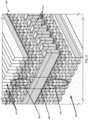
- FIG. 2 illustrates a detailed exemplary view of the memory partition 122 of FIG. 1 in accordance with certain embodiments.
- a memory partition 122 may include 3D crosspoint memory which may include phase change memory or other suitable memory types.
- a 3D crosspoint memory array 206 may comprise a transistor-less (e.g., at least with respect to the data storage elements of the memory) stackable crosspoint architecture in which memory cells 207 sit at the intersection of row address lines and column address lines arranged in a grid.
- row and column are terms of convenience used to provide a qualitative description of the arrangement of WLs and BLs in crosspoint memory.
- the cells of the 3D crosspoint memory array may be individually addressable.
- bit storage may be based on a change in bulk resistance of a 3D crosspoint memory cell.
- WL control logic 214 includes WL switch circuitry 220 and sense circuitry 222.
- WL control logic 214 is configured to receive target WL address(es) from memory partition controller 210 and to select one or more WLs for reading and/or writing operations.
- WL control logic 214 may be configured to select a target WL by coupling a WL select bias voltage to the target WL.
- WL control logic 214 may be configured to deselect a WL by decoupling the target WL from the WL select bias voltage and/or by coupling a WL deselect bias voltage (e.g., a neutral bias voltage) to the WL.
- WL control logic 214 may be coupled to a plurality of WLs 215 included in memory array 206.
- Each WL may be coupled to a number of memory cells corresponding to a number of BLs 217.
- WL switch circuitry 220 may include a plurality of switches, each switch configured to couple (or decouple) a respective WL, e.g., WL 215A, to a WL select bias voltage to select the respective WL 215A.
- BL control logic 216 includes BL switch circuitry 224.
- BL control logic 216 may also include sense circuitry, e.g., sense circuitry 222.
- BL control logic 216 is configured to select one or more BLs for reading and/or writing operations.
- BL control logic 216 may be configured to select a target BL by coupling a BL select bias voltage to the target BL.
- BL control logic 216 may be configured to deselect a BL by decoupling the target BL from the BL select bias voltage and/or by coupling a BL deselect bias voltage (e.g., a neutral bias voltage) to the BL.
- BL switch circuitry 224 is similar to WL switch circuitry 220 except BL switch circuitry 224 is configured to couple the BL select bias voltage to a target BL.
- Sense circuitry 222 is configured to detect the state of one or more sensed memory cells 207 (e.g., via the presence or absence of a snap back event during a sense interval), e.g., during a read operation. Sense circuitry 222 is configured to provide a logic level output related to the result of the read operation to, e.g., memory partition controller 210.
- the sense circuitry 222 may include a WL load connected to a WL electrode or gate, and a BL load connected to a BL electrode or gate.
- VDM may induce a current (i cell ) in the memory cell 207A dependent on a program state of the memory cell.
- a comparator such as a sense amplifier may compare i cell with a reference current in order to read a logic state of the memory cell. In this manner, an output of the sense amplifier/comparator may be indicative of a state of the target memory cell.
- a latch may be coupled to the output of the comparator to store the output of the read operation.
- each matrix of arrays there may be a number of sense amplifiers provided, with the sense circuitry 222 able to process up to a maximum number of sensed bits, such as 128 bits, from the sense amplifiers at one time.
- 128 memory cells may be sensed at one time by sense amplifiers of the sense circuitry 222.
- each memory cell (e.g., 300) includes a memory element configured to store information and a separate memory cell select device (e.g., selector) coupled to the memory element.
- Select devices may include ovonic threshold switches, diodes, bipolar junction transistors, field-effect transistors, etc.
- a first chalcogenide layer may comprise the memory element and a second chalcogenide layer may comprise the select device.
- the storage material 302 may include any suitable material programmable to a plurality of states.
- the storage material 302 may include a chalcogenide material comprising a chemical compound with at least one chalcogen ion, that is, an element from group 16 of the periodic table.
- the storage material 302 may include one or more of: sulfur (S), selenium (Se), or tellurium (Te).
- storage material 302 may comprise germanium (Ge), antimony (Sb), bismuth (Bi), lead (Pb), tin (Sn), indium (In), silver (Ag), arsenic (As), phosphorus (P), molybdenum (Mo), gallium (Ga), aluminum (Al), oxygen (O), nitrogen (N), chromium (Cr), gold (Au), niobium (Nb), palladium (Pd), cobalt (Co), vanadium (V), nickel (Ni), platinum (Pt), titanium (Ti), tungsten (W), tantalum (Ta), or other materials.
- OTS materials include Te-As-Ge-Si, Ge-Te-Pb, Ge-Se-Te, Al-As-Te, Se-As-Ge-Si, Se-As-Ge-C, Se-Te-Ge-Si, Ge-Sb-Te-Se, Ge-Bi-Te-Se, Ge-As-Sb-Se, Ge-As-Bi-Te, and Ge-As-Bi-Se, among others.
- programming the memory cell 300 causes the memory cell 300 to "threshold” or undergo a "threshold event.”
- a memory cell thresholds e.g., during application of a program pulse
- the memory cell undergoes a physical change that causes the memory cell to exhibit a certain threshold voltage in response to the application of a subsequent voltage (e.g., through application of a read pulse with a particular voltage magnitude and polarity).
- Programming the memory cell 300 can therefore involve applying a program pulse of a given polarity to induce a programming threshold event and application of current for a duration of time, which causes the memory cell 300 to exhibit a particular threshold voltage at a subsequent reading voltage of a same or different polarity.
- the storage material 302 is a self-selecting material that can be programmed by inducing a threshold event.
- Electrodes 308 are disposed between storage material 302 and access lines 304, 306. Electrodes 308 electrically couple access lines 304, 306 to storage material 302. Electrodes 308 can be composed of one or more conductive and/or semiconductive materials such as, for example: carbon (C), carbon nitride (C x N y ); n-doped polysilicon and p-doped polysilicon; metals including, Al, Cu, Ni, Mo, Cr, Co, Ru, Rh, Pd, Ag, Pt, Au, Ir, Ta, and W; conductive metal nitrides including TiN, TaN, WN, and TaCN; conductive metal silicides including tantalum silicides, tungsten silicides, nickel silicides, cobalt silicides and titanium silicides; conductive metal silicides nitrides including TiSiN and WSiN; conductive metal carbide nitrides including TiCN and WCN; conductive metal oxide
- the read controller 512 and the write controller 514 are configured to control read and write operations on the partitions 508, respectively.
- the read controller 512 and write controller 514 may be implemented as hardware, software, firmware, or a combination thereof.
- the read controller 512 and/or write controller 512 may be incorporated into or include any other suitable component, such as the microcontroller 502.
- the read controller 512 may perform a read operation in any suitable amount of time, such as 10-50 nanoseconds.
- the rank switching operation may take several clock cycles, such as 2-10 clock cycles, of a clock signal of the microcontroller 502. In the illustrative embodiment, rank switching takes up to 5 clock cycles.
- the clock corresponding to the clock cycles could have any suitable frequency, such as 50 megahertz to 2 gigahertz.
- the illustrative microcontroller 502 can send data to only one memory die 504 at a time.
- the delay may be any suitable value, such as 100-1,000 clock cycles. For example, in one embodiment, the delay is 602 clock cycles. It should be appreciated that the delay should be between the write operation to the partition 508, which may be delayed relative to the write operation sent over the command bus 516 for write operations that are stored in the buffer 510 before execution.
- the microcontroller 502 keeps track of when each write operation will be performed to each partition 508 and ensures that a read operation for that partition 508 will not be sent to the memory die 504 until after the minimum delay period has passed. In other embodiments, the microcontroller 502 may send read operations, and the chip controller 506 may delay the read operations until the minimum delay period has passed.
- the chip controller 506 can check if the write buffer 510 is empty. If it is, then the chip controller 506 can give the write command to the write controller 514, which can perform a write operation immediately (as long as the minimum amount of time has passed since the last write operation). If the write buffer 510 is not empty, then the chip controller 506 adds the write command to the buffer 510. In the illustrative embodiment, the microcontroller 502 should ensure that there is always room in the write buffer 510 for any write operations sent to the memory die 504. In other embodiments, the chip controller 506 may receive a write operation while the buffer 510 is full. In such embodiments, the chip controller 506 may, e.g., discard the new write operation, discard a previous write operation, send an error message to the microcontroller 502, set an error flag, etc.
- the microcontroller 502 arrange memory operations based on the size and space available in the buffer 510 of the target memory dies 504 in block 608.
- the microcontroller 502 may have a counter that tracks the number of operations that are (or, for future operations being ordered, will be) stored in the buffer 510 at any given time.
- the microcontroller 502 can increment to the counter every time it sends an operation to the memory die 504 and decrement the counter every time the memory die 504 performs a write operation, which, in the illustrative embodiment, are performed in a deterministic manner.
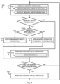
- a memory die 504 may perform a method 700 for performing memory operations.
- the method 700 begins in block 702, in which the memory die 504 receives a memory operation from the microcontroller 502.
- the memory die 504 may receive a memory read command in block 704 and may receive a memory write command in block 706.
- the memory die 504 receives a memory command on a command bus 516.
- the memory die 504 receives write data on a data bus 518.
- the memory die 504 may receive the write data on the data bus 518 at a predefined time relative to receiving the write command.
- the write data is received at the same time relative to a write command as the read data is sent on the data bus relative to a read command (see block 718 below).
- the memory die 504 checks if it is time for a memory write operation.
- the memory die 504 may check if enough time (or clock cycles) has passed since the last memory operation. In the illustrative embodiment, the memory die 504 may check if at least 16 clock cycles have passed. If enough time has passed and there is a write operation in the buffer 510, the memory die 504 performs a memory write operation in block 722. The method 700 then loops back to block 702 to receive another memory operation.
- the first memory die 504 can continue to complete the buffered write operations. For example, in time slot 8, the microcontroller 502 sends a write command to the second memory die 504, but the first memory die 504 is also performing the fourth write operation in a partition 508 at the same time.
- the write and read operations on the second memory die 504 can be completed in a similar manner as the write and read operations on the first memory die 504.
- the microcontroller 502 can switch back to the first memory die 504 and send the memory die 504 additional memory write operations, partially or fully filling up the empty buffer 510 in the memory die 504.
- the microcontroller 502 may need to either delay consecutive memory writes on the same memory die 504 switch ranks to a different memory die 504 for each of several consecutive memory writes. As such, a penalty of, e.g., five clock cycles may be present between each write operation.
- a relatively small buffer of, e.g., four slots the microcontroller 502 can perform four consecutive memory write operations without needing to switch ranks (or even more, as the memory die 504 will be processing the buffer 510 as the microcontroller 502 adds more items to the buffer 510, albeit at a slower rate).
- the buffer with four slots can, therefore, reduce the time lost in rank switching in certain circumstances by over 75%. Larger buffers 510 can further reduce the time lost in rank switching, but the amount of time saved decreases as the size of the buffer 510 increases. As such, a relatively small buffer 510 may be a reasonable compromise between added performance and reduced cost.
Landscapes
- Engineering & Computer Science (AREA)
- Theoretical Computer Science (AREA)
- Human Computer Interaction (AREA)
- Physics & Mathematics (AREA)
- General Engineering & Computer Science (AREA)
- General Physics & Mathematics (AREA)
- Chemical & Material Sciences (AREA)
- Crystallography & Structural Chemistry (AREA)
- Techniques For Improving Reliability Of Storages (AREA)
- Static Random-Access Memory (AREA)
- Semiconductor Memories (AREA)
Claims (13)
- Phasenwechsel-basierter Speicher-Die (504), der Folgendes umfasst:mehrere Partitionen (508); undeine Chipsteuerung (506), wobei die Chipsteuerung:eine erste Speicherschreiboperation zu einem ersten Zeitpunkt empfangen soll;eine zweite Speicherschreiboperation zu einem zweiten Zeitpunkt empfangen soll; underste Speicherschreibdaten, die der ersten Speicherschreiboperation entsprechen, an eine erste Partition der mehreren Partitionen senden soll;wobei der Phasenwechsel-basierte Speicher-Die eine minimale Zeitdauer benötigt, die nach dem Durchführen einer Speicherschreiboperation vor dem Durchführen einer nachfolgenden Schreiboperation zu verstreichen ist,dadurch gekennzeichnet, dass die Chipsteuerung ferner ausgelegt ist, um:zu bestimmen, dass eine Zeitdifferenz zwischen dem ersten Zeitpunkt und dem zweiten Zeitpunkt kleiner als die minimale Zeitdauer vor dem Durchführen einer nachfolgenden Schreiboperation ist; undals Reaktion auf das Bestimmen, dass die Zeitdifferenz zwischen dem ersten Zeitpunkt und dem zweiten Zeitpunkt kleiner als die minimale Zeitdauer vor dem Durchführen einer nachfolgenden Schreiboperation ist:zweite Speicherschreibdaten, die der zweiten Speicherschreiboperation entsprechen, in einem Puffer (510) des Phasenwechsel-basierten Speicher-Die zu speichern; undzweite Speicherschreibdaten von dem Puffer zu einer zweiten Partition der mehreren Partitionen zu senden, zumindest nachdem die minimale Zeitdauer vor dem Durchführen einer nachfolgenden Schreiboperation, nachdem die ersten Speicherschreibdaten an die erste Partition gesendet wurden, abgelaufen ist.
- Phasenwechsel-basierter Speicher-Die nach Anspruch 1, wobei die Chipsteuerung ferner:eine Speicherleseoperation nach der zweiten Speicherschreiboperation empfangen soll; undSpeicherlesedaten, die der Speicherleseoperation entsprechen, an eine dritte Partition der mehreren Partitionen senden soll, bevor die zweiten Speicherschreibdaten an die zweite Partition gesendet werden.
- Phasenwechsel-basierter Speicher-Die nach Anspruch 1, wobei die Chipsteuerung ferner:eine Speicherleseoperation nach der zweiten Speicherschreiboperation empfangen soll; undSpeicherlesedaten, die der Speicherleseoperation entsprechen, an eine dritte Partition der mehreren Partitionen gleichzeitig zu dem Zeitpunkt zu senden, an dem die zweiten Speicherschreibdaten an die zweite Partition gesendet werden.
- Phasenwechsel-basierter Speicher-Die nach einem der Ansprüche 1-3, wobei die Chipsteuerung ferner die ersten Speicherschreibdaten in weniger als 500 Nanosekunden in die erste Partition schreiben soll.
- Phasenwechsel-basierter Speicher-Die nach einem der Ansprüche 1-4, wobei der Phasenwechsel-basierte Speicher-Die 16-128 Partitionen aufweist.
- Phasenwechsel-basierter Speicher-Die nach einem der Ansprüche 1-5, wobei sich der Phasenwechsel-basierte Speicher-Die auf einem Dual-in-Line-Speichermodul (DIMM) befindet.
- Phasenwechsel-basierter Speicher-Die nach einem der Ansprüche 1-6, wobei sich der Phasenwechsel-basierte Speicher-Die auf einer Speichervorrichtung befindet.
- Phasenwechsel-basierter Speicher-Die nach einem der Ansprüche 1-7, wobei der Phasenwechsel-basierte Speicher-Die ein Taktsignal zwischen 100 und 500 Megahertz aufweist,
wobei die minimale durchschnittliche Zeitperiode zwischen Schreiboperationen zwischen 12 und 20 Taktzyklen des Taktsignals liegt. - Phasenwechsel-basierter Speicher-Die nach Anspruch 8, wobei eine Differenz zwischen dem ersten Zeitpunkt, der mit der ersten Speicherschreiboperation assoziiert ist, und dem zweiten Zeitpunkt, der mit der zweiten Speicherschreiboperation assoziiert ist, zwischen 2 und 10 Taktzyklen beträgt.
- Phasenwechsel-basierter Speicher-Die nach einem der Ansprüche 1-8, wobei die erste Speicherschreiboperation zwischen 4 und 64 Bytes schreiben soll, wobei die zweite Speicherschreiboperation zwischen 4 und 64 Bytes schreiben soll.
- Verfahren, das Folgendes umfasst:Empfangen, durch einen Phasenwechsel-basierten Speicher-Die (504) nach den Ansprüchen 1 bis 10, einer ersten Speicherschreiboperation zu einem ersten Zeitpunkt; undEmpfangen, durch den Phasenwechsel-basierten Speicher-Die, einer zweiten Speicherschreiboperation zu einem zweiten Zeitpunkt,wobei der Phasenwechsel-basierte Speicher-Die eine minimale Zeitdauer benötigt, die nach dem Durchführen einer Speicherschreiboperation vor dem Durchführen einer nachfolgenden Schreiboperation zu verstreichen ist,Senden, durch den Phasenwechsel-basierten Speicher-Die, erster Speicherschreibdaten, die der ersten Speicherschreiboperation entsprechen, an eine erste Partition mehrerer (508) des Phasenwechsel-basierten Speicher-Die;dadurch gekennzeichnet, dass das Verfahren ferner Folgendes umfasst:Bestimmen, dass eine Zeitdifferenz zwischen dem ersten Zeitpunkt und dem zweiten Zeitpunkt kleiner als die Zeitdauer vor dem Durchführen einer nachfolgenden Schreiboperation ist; undals Reaktion auf das Bestimmen, dass die Zeitdifferenz zwischen dem ersten Zeitpunkt und dem zweiten Zeitpunkt kleiner als die minimale Zeitdauer vor dem Durchführen einer nachfolgenden Schreiboperation ist:
Speichern, durch den Phasenwechsel-basierten Speicher-Die, zweiter Speicherschreibdaten, die der zweiten Speicherschreiboperation entsprechen, in einem Puffer (510) des Phasenwechsel-basierten Speicher-Die; und Senden, durch den Phasenwechsel-basierten Speicher-Die, der zweiten Speicherschreibdaten von dem Puffer zu einer zweiten Partition der mehreren Partitionen zumindest nachdem die minimale durchschnittliche Zeitperiode zwischen Schreiboperationen, nachdem die ersten Speicherschreibdaten an die erste Partition gesendet wurden, abgelaufen ist. - Verfahren nach Anspruch 11, das ferner Folgendes umfasst:Empfangen, durch den Phasenwechsel-basierten Speicher-Die, einer Speicherleseoperation nach der zweiten Speicherschreiboperation; undSenden, durch den Phasenwechsel-basierten Speicher-Die, von Speicherlesedaten, die der Speicherleseoperation entsprechen, an eine dritte Partition der mehreren Partitionen, bevor die zweiten Speicherschreibdaten an die zweite Partition gesendet werden.
- Verfahren nach Anspruch 11, das ferner Folgendes umfasst:Empfangen, durch den Phasenwechsel-basierten Speicher-Die, einer Speicherleseoperation nach der zweiten Speicherschreiboperation; undSenden, durch den Phasenwechsel-basierten Speicher-Die, von Speicherlesedaten, die der Speicherleseoperation entsprechen, an eine dritte Partition der mehreren Partitionen gleichzeitig zu dem Zeitpunkt, an dem die zweiten Speicherschreibdaten an die zweite Partition gesendet werden.
Applications Claiming Priority (1)
| Application Number | Priority Date | Filing Date | Title |
|---|---|---|---|
| US17/357,840 US12443362B2 (en) | 2021-06-24 | 2021-06-24 | Technologies for burst memory write operations |
Publications (2)
| Publication Number | Publication Date |
|---|---|
| EP4109452A1 EP4109452A1 (de) | 2022-12-28 |
| EP4109452B1 true EP4109452B1 (de) | 2025-04-16 |
Family
ID=80928715
Family Applications (1)
| Application Number | Title | Priority Date | Filing Date |
|---|---|---|---|
| EP22163142.7A Active EP4109452B1 (de) | 2021-06-24 | 2022-03-21 | Technologien für burst-speicher-schreibvorgänge |
Country Status (4)
| Country | Link |
|---|---|
| US (1) | US12443362B2 (de) |
| EP (1) | EP4109452B1 (de) |
| KR (1) | KR20230001015A (de) |
| CN (1) | CN115525213A (de) |
Family Cites Families (7)
| Publication number | Priority date | Publication date | Assignee | Title |
|---|---|---|---|---|
| US20160357456A1 (en) | 2015-06-03 | 2016-12-08 | Kabushiki Kaisha Toshiba | Memory device that divides write data into a plurality of data portions for data writing |
| KR102333220B1 (ko) * | 2015-09-24 | 2021-12-01 | 삼성전자주식회사 | 불휘발성 메모리 시스템의 동작 방법 |
| US10043577B2 (en) | 2016-03-08 | 2018-08-07 | Toshiba Memory Corporation | Semiconductor memory device |
| US20170308296A1 (en) | 2016-04-22 | 2017-10-26 | Hewlett Packard Enterprise Development Lp | Staging write requests |
| US10684795B2 (en) | 2016-07-25 | 2020-06-16 | Toshiba Memory Corporation | Storage device and storage control method |
| KR102810527B1 (ko) * | 2019-09-23 | 2025-05-22 | 삼성전자주식회사 | 스토리지 장치 및 그것의 동작 방법 |
| JP2021114038A (ja) * | 2020-01-16 | 2021-08-05 | キオクシア株式会社 | メモリシステムおよび制御方法 |
-
2021
- 2021-06-24 US US17/357,840 patent/US12443362B2/en active Active
-
2022
- 2022-03-21 EP EP22163142.7A patent/EP4109452B1/de active Active
- 2022-03-22 KR KR1020220035191A patent/KR20230001015A/ko active Pending
- 2022-05-16 CN CN202210528422.0A patent/CN115525213A/zh active Pending
Also Published As
| Publication number | Publication date |
|---|---|
| US12443362B2 (en) | 2025-10-14 |
| US20220413740A1 (en) | 2022-12-29 |
| KR20230001015A (ko) | 2023-01-03 |
| EP4109452A1 (de) | 2022-12-28 |
| CN115525213A (zh) | 2022-12-27 |
Similar Documents
| Publication | Publication Date | Title |
|---|---|---|
| US12153823B2 (en) | Multi-level memory programming and readout | |
| US12588430B2 (en) | Elemental composition tuning for chalcogenide based memory arranged in a plurality of decks | |
| EP4050607A1 (de) | Technologien zur steuerung des stroms durch speicherzellen | |
| US12361979B2 (en) | Technologies for on-memory die voltage regulator | |
| US12277985B2 (en) | Technologies for repair of memory with access lines | |
| US20230276639A1 (en) | Metal silicide layer for memory array | |
| EP4109454A1 (de) | Kreuzpunkt-speicherleseverfahren zur minderung von driftfehlern | |
| US11404105B2 (en) | Write disturb refresh rate reduction using write history buffer | |
| US12417797B2 (en) | NOR gate based local access line deselect signal generation | |
| US12573453B2 (en) | Technologies for dynamic current mirror biasing for memory cells | |
| US12501628B2 (en) | Memory comprising conductive ferroelectric material in series with dielectric material | |
| US12475945B2 (en) | Spike based programming of a memory cell to reset state | |
| EP4109452A1 (de) | Technologien für burst-speicher-schreibvorgänge | |
| US12119064B2 (en) | Binary to ternary convertor for multilevel memory | |
| US20220180934A1 (en) | Read window budget optimization for three dimensional crosspoint memory | |
| US12512155B2 (en) | Technologies for current biasing for three-dimensional crosspoint memory cells | |
| US20230317154A1 (en) | Technologies for dynamic biasing for memory cells | |
| US20230363297A1 (en) | Technologies for semiconductor devices including amorphous silicon | |
| EP4134956A1 (de) | Spannungsdetektor für sequenz zum herunterfahren der versorgung | |
| US12254946B2 (en) | Multi-deck non-volatile memory architecture with reduced termination tile area | |
| US12394461B2 (en) | Multi-deck non-volatile memory architecture with improved address line driver circuitry | |
| US20230354723A1 (en) | Structure and method of depositing memory cell electrode materials with low intrinsic roughness | |
| US20230380307A1 (en) | Bilayer encapsulation of a memory cell | |
| US20230209834A1 (en) | Reliable electrode for memory cells | |
| US20230157035A1 (en) | Multi-layer interconnect |
Legal Events
| Date | Code | Title | Description |
|---|---|---|---|
| PUAI | Public reference made under article 153(3) epc to a published international application that has entered the european phase |
Free format text: ORIGINAL CODE: 0009012 |
|
| STAA | Information on the status of an ep patent application or granted ep patent |
Free format text: STATUS: THE APPLICATION HAS BEEN PUBLISHED |
|
| AK | Designated contracting states |
Kind code of ref document: A1 Designated state(s): AL AT BE BG CH CY CZ DE DK EE ES FI FR GB GR HR HU IE IS IT LI LT LU LV MC MK MT NL NO PL PT RO RS SE SI SK SM TR |
|
| STAA | Information on the status of an ep patent application or granted ep patent |
Free format text: STATUS: REQUEST FOR EXAMINATION WAS MADE |
|
| 17P | Request for examination filed |
Effective date: 20230623 |
|
| RBV | Designated contracting states (corrected) |
Designated state(s): AL AT BE BG CH CY CZ DE DK EE ES FI FR GB GR HR HU IE IS IT LI LT LU LV MC MK MT NL NO PL PT RO RS SE SI SK SM TR |
|
| GRAP | Despatch of communication of intention to grant a patent |
Free format text: ORIGINAL CODE: EPIDOSNIGR1 |
|
| STAA | Information on the status of an ep patent application or granted ep patent |
Free format text: STATUS: GRANT OF PATENT IS INTENDED |
|
| INTG | Intention to grant announced |
Effective date: 20241114 |
|
| GRAS | Grant fee paid |
Free format text: ORIGINAL CODE: EPIDOSNIGR3 |
|
| GRAA | (expected) grant |
Free format text: ORIGINAL CODE: 0009210 |
|
| STAA | Information on the status of an ep patent application or granted ep patent |
Free format text: STATUS: THE PATENT HAS BEEN GRANTED |
|
| AK | Designated contracting states |
Kind code of ref document: B1 Designated state(s): AL AT BE BG CH CY CZ DE DK EE ES FI FR GB GR HR HU IE IS IT LI LT LU LV MC MK MT NL NO PL PT RO RS SE SI SK SM TR |
|
| REG | Reference to a national code |
Ref country code: GB Ref legal event code: FG4D |
|
| REG | Reference to a national code |
Ref country code: CH Ref legal event code: EP |
|
| REG | Reference to a national code |
Ref country code: IE Ref legal event code: FG4D |
|
| REG | Reference to a national code |
Ref country code: DE Ref legal event code: R096 Ref document number: 602022013092 Country of ref document: DE |
|
| P01 | Opt-out of the competence of the unified patent court (upc) registered |
Free format text: CASE NUMBER: APP_20028/2025 Effective date: 20250428 |
|
| REG | Reference to a national code |
Ref country code: NL Ref legal event code: FP |
|
| REG | Reference to a national code |
Ref country code: AT Ref legal event code: MK05 Ref document number: 1786346 Country of ref document: AT Kind code of ref document: T Effective date: 20250416 |
|
| PG25 | Lapsed in a contracting state [announced via postgrant information from national office to epo] |
Ref country code: FI Free format text: LAPSE BECAUSE OF FAILURE TO SUBMIT A TRANSLATION OF THE DESCRIPTION OR TO PAY THE FEE WITHIN THE PRESCRIBED TIME-LIMIT Effective date: 20250416 Ref country code: PT Free format text: LAPSE BECAUSE OF FAILURE TO SUBMIT A TRANSLATION OF THE DESCRIPTION OR TO PAY THE FEE WITHIN THE PRESCRIBED TIME-LIMIT Effective date: 20250818 Ref country code: ES Free format text: LAPSE BECAUSE OF FAILURE TO SUBMIT A TRANSLATION OF THE DESCRIPTION OR TO PAY THE FEE WITHIN THE PRESCRIBED TIME-LIMIT Effective date: 20250416 |
|
| REG | Reference to a national code |
Ref country code: LT Ref legal event code: MG9D |
|
| PG25 | Lapsed in a contracting state [announced via postgrant information from national office to epo] |
Ref country code: GR Free format text: LAPSE BECAUSE OF FAILURE TO SUBMIT A TRANSLATION OF THE DESCRIPTION OR TO PAY THE FEE WITHIN THE PRESCRIBED TIME-LIMIT Effective date: 20250717 Ref country code: NO Free format text: LAPSE BECAUSE OF FAILURE TO SUBMIT A TRANSLATION OF THE DESCRIPTION OR TO PAY THE FEE WITHIN THE PRESCRIBED TIME-LIMIT Effective date: 20250716 |
|
| PG25 | Lapsed in a contracting state [announced via postgrant information from national office to epo] |
Ref country code: PL Free format text: LAPSE BECAUSE OF FAILURE TO SUBMIT A TRANSLATION OF THE DESCRIPTION OR TO PAY THE FEE WITHIN THE PRESCRIBED TIME-LIMIT Effective date: 20250416 |
|
| PG25 | Lapsed in a contracting state [announced via postgrant information from national office to epo] |
Ref country code: BG Free format text: LAPSE BECAUSE OF FAILURE TO SUBMIT A TRANSLATION OF THE DESCRIPTION OR TO PAY THE FEE WITHIN THE PRESCRIBED TIME-LIMIT Effective date: 20250416 |
|
| PG25 | Lapsed in a contracting state [announced via postgrant information from national office to epo] |
Ref country code: HR Free format text: LAPSE BECAUSE OF FAILURE TO SUBMIT A TRANSLATION OF THE DESCRIPTION OR TO PAY THE FEE WITHIN THE PRESCRIBED TIME-LIMIT Effective date: 20250416 |
|
| PG25 | Lapsed in a contracting state [announced via postgrant information from national office to epo] |
Ref country code: AT Free format text: LAPSE BECAUSE OF FAILURE TO SUBMIT A TRANSLATION OF THE DESCRIPTION OR TO PAY THE FEE WITHIN THE PRESCRIBED TIME-LIMIT Effective date: 20250416 |
|
| PG25 | Lapsed in a contracting state [announced via postgrant information from national office to epo] |
Ref country code: RS Free format text: LAPSE BECAUSE OF FAILURE TO SUBMIT A TRANSLATION OF THE DESCRIPTION OR TO PAY THE FEE WITHIN THE PRESCRIBED TIME-LIMIT Effective date: 20250716 |
|
| PG25 | Lapsed in a contracting state [announced via postgrant information from national office to epo] |
Ref country code: IS Free format text: LAPSE BECAUSE OF FAILURE TO SUBMIT A TRANSLATION OF THE DESCRIPTION OR TO PAY THE FEE WITHIN THE PRESCRIBED TIME-LIMIT Effective date: 20250816 |
|
| PG25 | Lapsed in a contracting state [announced via postgrant information from national office to epo] |
Ref country code: LV Free format text: LAPSE BECAUSE OF FAILURE TO SUBMIT A TRANSLATION OF THE DESCRIPTION OR TO PAY THE FEE WITHIN THE PRESCRIBED TIME-LIMIT Effective date: 20250416 |
|
| PG25 | Lapsed in a contracting state [announced via postgrant information from national office to epo] |
Ref country code: SM Free format text: LAPSE BECAUSE OF FAILURE TO SUBMIT A TRANSLATION OF THE DESCRIPTION OR TO PAY THE FEE WITHIN THE PRESCRIBED TIME-LIMIT Effective date: 20250416 Ref country code: DK Free format text: LAPSE BECAUSE OF FAILURE TO SUBMIT A TRANSLATION OF THE DESCRIPTION OR TO PAY THE FEE WITHIN THE PRESCRIBED TIME-LIMIT Effective date: 20250416 |
|
| REG | Reference to a national code |
Ref country code: DE Ref legal event code: R097 Ref document number: 602022013092 Country of ref document: DE |
|
| PG25 | Lapsed in a contracting state [announced via postgrant information from national office to epo] |
Ref country code: CZ Free format text: LAPSE BECAUSE OF FAILURE TO SUBMIT A TRANSLATION OF THE DESCRIPTION OR TO PAY THE FEE WITHIN THE PRESCRIBED TIME-LIMIT Effective date: 20250416 |
|
| PG25 | Lapsed in a contracting state [announced via postgrant information from national office to epo] |
Ref country code: EE Free format text: LAPSE BECAUSE OF FAILURE TO SUBMIT A TRANSLATION OF THE DESCRIPTION OR TO PAY THE FEE WITHIN THE PRESCRIBED TIME-LIMIT Effective date: 20250416 |
|
| PG25 | Lapsed in a contracting state [announced via postgrant information from national office to epo] |
Ref country code: SK Free format text: LAPSE BECAUSE OF FAILURE TO SUBMIT A TRANSLATION OF THE DESCRIPTION OR TO PAY THE FEE WITHIN THE PRESCRIBED TIME-LIMIT Effective date: 20250416 |
|
| PG25 | Lapsed in a contracting state [announced via postgrant information from national office to epo] |
Ref country code: IT Free format text: LAPSE BECAUSE OF FAILURE TO SUBMIT A TRANSLATION OF THE DESCRIPTION OR TO PAY THE FEE WITHIN THE PRESCRIBED TIME-LIMIT Effective date: 20250416 |
|
| PLBE | No opposition filed within time limit |
Free format text: ORIGINAL CODE: 0009261 |
|
| STAA | Information on the status of an ep patent application or granted ep patent |
Free format text: STATUS: NO OPPOSITION FILED WITHIN TIME LIMIT |
|
| REG | Reference to a national code |
Ref country code: CH Ref legal event code: L10 Free format text: ST27 STATUS EVENT CODE: U-0-0-L10-L00 (AS PROVIDED BY THE NATIONAL OFFICE) Effective date: 20260225 |
|
| PGFP | Annual fee paid to national office [announced via postgrant information from national office to epo] |
Ref country code: NL Payment date: 20260227 Year of fee payment: 5 |
|
| 26N | No opposition filed |
Effective date: 20260119 |
|
| PGFP | Annual fee paid to national office [announced via postgrant information from national office to epo] |
Ref country code: GB Payment date: 20260223 Year of fee payment: 5 |
|
| PGFP | Annual fee paid to national office [announced via postgrant information from national office to epo] |
Ref country code: DE Payment date: 20260102 Year of fee payment: 5 |
|
| PGFP | Annual fee paid to national office [announced via postgrant information from national office to epo] |
Ref country code: FR Payment date: 20260223 Year of fee payment: 5 |