EP4109559A1 - Bipolartransistor mit isolierter steuerelektrode, motorsteuereinheit für ein kraftfahrzeug - Google Patents
Bipolartransistor mit isolierter steuerelektrode, motorsteuereinheit für ein kraftfahrzeug Download PDFInfo
- Publication number
- EP4109559A1 EP4109559A1 EP20926062.9A EP20926062A EP4109559A1 EP 4109559 A1 EP4109559 A1 EP 4109559A1 EP 20926062 A EP20926062 A EP 20926062A EP 4109559 A1 EP4109559 A1 EP 4109559A1
- Authority
- EP
- European Patent Office
- Prior art keywords
- layer
- bipolar transistor
- metal electrode
- insulated gate
- gate bipolar
- Prior art date
- Legal status (The legal status is an assumption and is not a legal conclusion. Google has not performed a legal analysis and makes no representation as to the accuracy of the status listed.)
- Pending
Links
- 239000002184 metal Substances 0.000 claims abstract description 113
- 239000010410 layer Substances 0.000 claims description 157
- 239000011229 interlayer Substances 0.000 claims description 4
- 239000000243 solution Substances 0.000 description 15
- 239000004065 semiconductor Substances 0.000 description 8
- 238000002955 isolation Methods 0.000 description 6
- 238000011084 recovery Methods 0.000 description 5
- 238000006243 chemical reaction Methods 0.000 description 4
- 238000002360 preparation method Methods 0.000 description 4
- 238000005516 engineering process Methods 0.000 description 3
- 230000005669 field effect Effects 0.000 description 3
- 239000002131 composite material Substances 0.000 description 2
- 238000010586 diagram Methods 0.000 description 2
- 230000010354 integration Effects 0.000 description 2
- 238000012986 modification Methods 0.000 description 2
- 230000004048 modification Effects 0.000 description 2
- 238000005476 soldering Methods 0.000 description 2
- 238000009792 diffusion process Methods 0.000 description 1
- 238000002347 injection Methods 0.000 description 1
- 239000007924 injection Substances 0.000 description 1
- 238000000034 method Methods 0.000 description 1
- 229910021420 polycrystalline silicon Inorganic materials 0.000 description 1
Images

Classifications
-
- H—ELECTRICITY
- H10—SEMICONDUCTOR DEVICES; ELECTRIC SOLID-STATE DEVICES NOT OTHERWISE PROVIDED FOR
- H10D—INORGANIC ELECTRIC SEMICONDUCTOR DEVICES
- H10D30/00—Field-effect transistors [FET]
- H10D30/60—Insulated-gate field-effect transistors [IGFET]
- H10D30/64—Double-diffused metal-oxide semiconductor [DMOS] FETs
- H10D30/66—Vertical DMOS [VDMOS] FETs
- H10D30/668—Vertical DMOS [VDMOS] FETs having trench gate electrodes, e.g. UMOS transistors
-
- H—ELECTRICITY
- H10—SEMICONDUCTOR DEVICES; ELECTRIC SOLID-STATE DEVICES NOT OTHERWISE PROVIDED FOR
- H10D—INORGANIC ELECTRIC SEMICONDUCTOR DEVICES
- H10D12/00—Bipolar devices controlled by the field effect, e.g. insulated-gate bipolar transistors [IGBT]
- H10D12/411—Insulated-gate bipolar transistors [IGBT]
-
- H—ELECTRICITY
- H10—SEMICONDUCTOR DEVICES; ELECTRIC SOLID-STATE DEVICES NOT OTHERWISE PROVIDED FOR
- H10D—INORGANIC ELECTRIC SEMICONDUCTOR DEVICES
- H10D12/00—Bipolar devices controlled by the field effect, e.g. insulated-gate bipolar transistors [IGBT]
- H10D12/411—Insulated-gate bipolar transistors [IGBT]
- H10D12/441—Vertical IGBTs
- H10D12/461—Vertical IGBTs having non-planar surfaces, e.g. having trenches, recesses or pillars in the surfaces of the emitter, base or collector regions
- H10D12/481—Vertical IGBTs having non-planar surfaces, e.g. having trenches, recesses or pillars in the surfaces of the emitter, base or collector regions having gate structures on slanted surfaces, on vertical surfaces, or in grooves, e.g. trench gate IGBTs
-
- H—ELECTRICITY
- H10—SEMICONDUCTOR DEVICES; ELECTRIC SOLID-STATE DEVICES NOT OTHERWISE PROVIDED FOR
- H10D—INORGANIC ELECTRIC SEMICONDUCTOR DEVICES
- H10D62/00—Semiconductor bodies, or regions thereof, of devices having potential barriers
- H10D62/10—Shapes, relative sizes or dispositions of the regions of the semiconductor bodies; Shapes of the semiconductor bodies
- H10D62/102—Constructional design considerations for preventing surface leakage or controlling electric field concentration
- H10D62/103—Constructional design considerations for preventing surface leakage or controlling electric field concentration for increasing or controlling the breakdown voltage of reverse-biased devices
- H10D62/105—Constructional design considerations for preventing surface leakage or controlling electric field concentration for increasing or controlling the breakdown voltage of reverse-biased devices by having particular doping profiles, shapes or arrangements of PN junctions; by having supplementary regions, e.g. junction termination extension [JTE]
- H10D62/109—Reduced surface field [RESURF] PN junction structures
- H10D62/111—Multiple RESURF structures, e.g. double RESURF or 3D-RESURF structures
-
- H—ELECTRICITY
- H10—SEMICONDUCTOR DEVICES; ELECTRIC SOLID-STATE DEVICES NOT OTHERWISE PROVIDED FOR
- H10D—INORGANIC ELECTRIC SEMICONDUCTOR DEVICES
- H10D62/00—Semiconductor bodies, or regions thereof, of devices having potential barriers
- H10D62/10—Shapes, relative sizes or dispositions of the regions of the semiconductor bodies; Shapes of the semiconductor bodies
- H10D62/17—Semiconductor regions connected to electrodes not carrying current to be rectified, amplified or switched, e.g. channel regions
- H10D62/393—Body regions of DMOS transistors or IGBTs
-
- H—ELECTRICITY
- H10—SEMICONDUCTOR DEVICES; ELECTRIC SOLID-STATE DEVICES NOT OTHERWISE PROVIDED FOR
- H10D—INORGANIC ELECTRIC SEMICONDUCTOR DEVICES
- H10D64/00—Electrodes of devices having potential barriers
- H10D64/20—Electrodes characterised by their shapes, relative sizes or dispositions
- H10D64/23—Electrodes carrying the current to be rectified, amplified, oscillated or switched, e.g. sources, drains, anodes or cathodes
- H10D64/231—Emitter or collector electrodes for bipolar transistors
-
- H—ELECTRICITY
- H10—SEMICONDUCTOR DEVICES; ELECTRIC SOLID-STATE DEVICES NOT OTHERWISE PROVIDED FOR
- H10D—INORGANIC ELECTRIC SEMICONDUCTOR DEVICES
- H10D64/00—Electrodes of devices having potential barriers
- H10D64/20—Electrodes characterised by their shapes, relative sizes or dispositions
- H10D64/23—Electrodes carrying the current to be rectified, amplified, oscillated or switched, e.g. sources, drains, anodes or cathodes
- H10D64/232—Emitter electrodes for IGBTs
-
- H—ELECTRICITY
- H10—SEMICONDUCTOR DEVICES; ELECTRIC SOLID-STATE DEVICES NOT OTHERWISE PROVIDED FOR
- H10D—INORGANIC ELECTRIC SEMICONDUCTOR DEVICES
- H10D64/00—Electrodes of devices having potential barriers
- H10D64/20—Electrodes characterised by their shapes, relative sizes or dispositions
- H10D64/27—Electrodes not carrying the current to be rectified, amplified, oscillated or switched, e.g. gates
- H10D64/281—Base electrodes for bipolar transistors
-
- H—ELECTRICITY
- H10—SEMICONDUCTOR DEVICES; ELECTRIC SOLID-STATE DEVICES NOT OTHERWISE PROVIDED FOR
- H10D—INORGANIC ELECTRIC SEMICONDUCTOR DEVICES
- H10D84/00—Integrated devices formed in or on semiconductor substrates that comprise only semiconducting layers, e.g. on Si wafers or on GaAs-on-Si wafers
- H10D84/101—Integrated devices comprising main components and built-in components, e.g. IGBT having built-in freewheel diode
- H10D84/141—VDMOS having built-in components
-
- H—ELECTRICITY
- H02—GENERATION; CONVERSION OR DISTRIBUTION OF ELECTRIC POWER
- H02P—CONTROL OR REGULATION OF ELECTRIC MOTORS, ELECTRIC GENERATORS OR DYNAMO-ELECTRIC CONVERTERS; CONTROLLING TRANSFORMERS, REACTORS OR CHOKE COILS
- H02P25/00—Arrangements or methods for the control of AC motors characterised by the kind of AC motor or by structural details
- H02P25/16—Arrangements or methods for the control of AC motors characterised by the kind of AC motor or by structural details characterised by the circuit arrangement or by the kind of wiring
-
- H—ELECTRICITY
- H10—SEMICONDUCTOR DEVICES; ELECTRIC SOLID-STATE DEVICES NOT OTHERWISE PROVIDED FOR
- H10D—INORGANIC ELECTRIC SEMICONDUCTOR DEVICES
- H10D62/00—Semiconductor bodies, or regions thereof, of devices having potential barriers
- H10D62/10—Shapes, relative sizes or dispositions of the regions of the semiconductor bodies; Shapes of the semiconductor bodies
- H10D62/13—Semiconductor regions connected to electrodes carrying current to be rectified, amplified or switched, e.g. source or drain regions
- H10D62/141—Anode or cathode regions of thyristors; Collector or emitter regions of gated bipolar-mode devices, e.g. of IGBTs
- H10D62/142—Anode regions of thyristors or collector regions of gated bipolar-mode devices
Definitions
- This application relates to the field of electrical technologies, and in particular, to an insulated gate bipolar transistor, a motor control unit, and a vehicle.
- An MCU (Motor Control Unit, motor control unit) of an electric vehicle usually uses an IGBT (Insulated Gate Bipolar Transistor, insulated gate bipolar transistor) as a switching element, to convert a direct current (DC) output by a battery into an alternating current (AC) to drive a motor.
- IGBT Insulated Gate Bipolar Transistor, insulated gate bipolar transistor
- the IGBT is a composite fully-controlled voltage-driven power semiconductor device including a MOSFET (Metal-Oxide-Semiconductor Field-Effect Transistor, metal-oxide-semiconductor field-effect transistor) and a BJT (bipolar junction transistor).
- MOSFET Metal-Oxide-Semiconductor Field-Effect Transistor, metal-oxide-semiconductor field-effect transistor
- BJT bipolar junction transistor
- a device designer performs chip integration on the IGBT and the FRD, and proposes an RC-IGBT (Reverse-Conduction Insulated Gate Bipolar Transistor, reverse-conduction IGBT) structure, so that the device has a higher cutoff speed and a better Vcesat-Eoff tradeoff relationship.
- the MCU of the electric vehicle operates in a light load state most of time. Regardless of whether an RC-IGBT or an SJ-RC-IGBT is used as the switching element, a control chip cannot accurately control an operating mode of the switching element based on an operating status of the MCU, affecting further improvement of conversion efficiency of the MCU.
- This application provides an insulated gate bipolar transistor, a motor control unit, and a vehicle, to improve a control effect of the insulated gate bipolar transistor.
- an insulated gate bipolar transistor is provided.
- the insulated gate bipolar transistor is applied to a motor control unit.
- a laminated multi-layer structure of the insulated gate bipolar transistor includes, for example, an IGBT device structure feature layer, an SJ device structure feature layer, and an RC-IGBT device structure feature layer, and the IGBT device structure feature layer and the RC-IGBT device structure feature layer are respectively arranged on two sides of the SJ device structure feature layer.
- the RC-IGBT device structure feature layer includes a collector and a drain that are disposed at a same layer.
- the insulated gate bipolar transistor further includes a first metal electrode laminated with and electrically connected to the collector, and a second metal electrode laminated with and electrically connected to the drain, and the first metal electrode is electrically isolated from the second metal electrode.
- the first metal electrode and the second metal electrode may be respectively connected to the collector and the drain, and power may be separately supplied to the collector and the drain, so that a power supply manner of the insulated gate bipolar transistor is added, thereby improving a control manner of the insulated gate bipolar transistor.
- the SJ device structure feature layer includes a drift layer, a super-junction structure layer, and a buffer layer that are laminated, and the super-junction structure layer is located between the drift layer and the buffer layer.
- the drift layer is connected to the IGBT device structure feature layer.
- the buffer layer is connected to the collector and the drain.
- the buffer layer is an N-type buffer layer.
- the drift layer is an N-drift layer.
- the super-junction structure layer includes a plurality of N-drift layers and a plurality of P-drift layers, the plurality of N-drift layers and the plurality of P-drift layers are alternately arranged in a first direction, and the first direction is perpendicular to a second direction.
- the second direction is a direction in which the IGBT device structure feature layer is laminated with the SJ device structure feature layer.
- the IGBT device structure feature layer includes:
- the first metal electrode is in ohmic contact with the collector; and/or the second metal electrode is in ohmic contact with the drain.
- the first metal electrode is separated from the second metal electrode by a specified distance.
- a plurality of collectors and a plurality of drains there are a plurality of collectors and a plurality of drains, and the plurality of collectors and the plurality of drains are alternately arranged.
- first metal electrodes are in a one-to-one correspondence with the collectors
- second metal electrodes are in a one-to-one correspondence with the drains
- any adjacent first metal electrode and second metal electrode are electrically isolated from each other.
- a motor control unit includes a power module and the insulated gate bipolar transistor that is connected to the power module and that is described in any one of the foregoing solutions.
- the first metal electrode and the second metal electrode may be respectively connected to the collector and the drain, and power may be separately supplied to the collector and the drain, so that a power supply manner of the insulated gate bipolar transistor is added, thereby improving a control manner of the insulated gate bipolar transistor.
- a vehicle includes a motor and a motor control unit that is connected to the motor and that is described in any one of the foregoing solutions.
- the first metal electrode and the second metal electrode may be respectively connected to the collector and the drain, and power may be separately supplied to the collector and the drain, so that a power supply manner of the insulated gate bipolar transistor is added, thereby improving a control manner of the insulated gate bipolar transistor.
- an MCU Motor Control Unit, motor control unit
- an IGBT Insulated Gate Bipolar Transistor, insulated gate bipolar transistor
- the IGBT is a composite fully-controlled voltage-driven power semiconductor device including a MOSFET (metal-oxide-semiconductor field-effect transistor) and a BJT (bipolar junction transistor).
- the IGBT has advantages of both a high input impedance of the MOSFET and a low conduction voltage drop of the BJT, and is a power semiconductor device suitable for medium and high power applications.
- the IGBT needs to be used together with an FRD.
- a device designer performs chip integration on the IGBT and the FRD, and proposes an RC-IGBT structure, so that the device has a higher cutoff speed and a better Vcesat-Eoff tradeoff relationship.
- an embodiment of this application provides an insulated gate bipolar transistor.
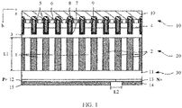
- FIG. 1 is a cross-sectional view of an insulated gate bipolar transistor according to an embodiment of this application.
- the insulated gate bipolar transistor provided in this embodiment of this application mainly includes three structures: an IGBT device structure feature layer 10, an SJ device structure feature layer 20, and an RC-IGBT device structure feature layer 30.
- the IGBT device structure feature layer 10, the SJ device structure feature layer 20, and the RC-IGBT device structure feature layer 30 are laminated in a vertical direction in FIG. 1 , and the IGBT device structure feature layer 10 and the RC-IGBT device structure feature layer 30 are respectively arranged on two sides of the SJ device structure feature layer 20.
- the second direction b is a direction in which the IGBT device structure feature layer 10 and the SJ device structure feature layer 20 are laminated, and the first direction a is perpendicular to the second direction b.
- the SJ device structure feature layer 20 mainly includes a drift layer 3, a super-junction structure layer, and a buffer layer 11 that are laminated, and the super-junction structure layer is located between the drift layer 3 and the buffer layer 11.
- the buffer layer 11 is an N-type buffer layer.
- a super-junction structure and the drift layer 3 are formed on a first surface of the buffer layer 11.
- the super-junction structure includes a plurality of N-drift layers 1 and a plurality of P-drift layers 2, and the plurality of N-drift layers 1 and the plurality of P-drift layers 2 are alternately arranged in the first direction a.
- the N-drift layer 1 and the P-drift layer 2 are formed by using injection, diffusion, and epitaxial growth processes, and both a thickness of the N-drift layer 1 and a thickness of the P-drift layer 2 are set to L1.
- the drift layer 3 on the super-junction structure is an N-drift layer, and the drift layer 3 is formed on a surface that is of the super-junction structure and that is away from the buffer layer 11.
- the IGBT device structure feature layer 10 is connected to the drift layer 3.
- the IGBT device structure feature layer 10 includes: a P base layer 4 laminated with the drift layer 3 in the first direction a, and a front emitter 10 laminated with the P base layer 4; and a plurality of gates 8 that are penetrated through the P base layer 4 and inserted into the N-drift layer 3, an insulating gate film 7 that wraps each gate 8, an interlayer insulating film 9 that insulates each gate 8 from the front emitter 10, and an N emitter layer 5 and a P+ contact layer 6 that are disposed on a surface of the P base layer 4.
- the P base layer 4 is formed on the drift layer 3, and the N emitter layer 5 and the P+ contact layer 6 are formed on the surface of the P base layer 4.
- a trench is formed from a surface of the N emitter layer 5 to a midway close to the drift layer 3 through the P base layer 4, and the gate 8 is formed in the trench by interposing the insulating gate film 7 between the gate 8 and the trench.
- the insulating gate film 7 is a gate oxide layer, and a polycrystalline silicon gate may be used as the gate 8.
- the front emitter 10 is formed on the P+ contact layer 6, and the gate 8 is insulated from the front emitter 10 by using the interlayer insulating film 9.
- the RC-IGBT device structure feature layer 30 includes a collector 12 and a drain 13 that are disposed at a same layer.
- the collector 12 and the drain 13 are formed on a second surface of the buffer layer 11 in the first direction a in FIG. 1 .
- a first metal electrode 15 and a second metal electrode 14 are formed on back surfaces of the collector 12 and the drain 13. The first metal electrode 15 is laminated with and electrically connected to the collector 12, the second metal electrode 14 is laminated with and electrically connected to the drain 13, and the first metal electrode 15 is electrically isolated from the second metal electrode 14.
- the first metal electrode 15 is in ohmic contact with the collector 12 to ensure an electrical connection effect between the first metal electrode 15 and the collector 12.
- electrical connection between the first metal electrode 15 and the collector 12 may be implemented through soldering, or by directly forming the first metal electrode 15 on the collector 12.
- the second metal electrode 14 is in ohmic contact with the drain 13 to ensure an electrical connection effect between the second metal electrode 14 and the drain 13.
- electrical connection between the second metal electrode 14 and the drain 13 may be implemented through soldering, or by directly forming the second metal electrode 14 on the drain 13.
- the first metal electrode 15 is separated from the second metal electrode 14 by a specified distance, to ensure an isolation degree between the first metal electrode 15 and the second metal electrode 14.
- the specified distance indicates a horizontal distance L2, in the first direction a, between an end portion of the first metal electrode 15 and an end portion of the second metal electrode 14 that are close to each other.
- L2 may be determined based on an actual design, and is not specifically limited in this application, provided that an isolation degree between the first metal electrode 15 and the second metal electrode 14 can be ensured.
- the first metal electrode 15 may be specifically isolated from the second metal electrode 14 in different manners.
- the first metal electrode 15 may cover the collector 12 and have an area equal to an area of the collector 12, and the second metal electrode 14 may cover the drain 13 and have an area less than an area of the drain 13; the first metal electrode 15 may cover the collector 12 and have an area less than an area of the collector 12, and the second metal electrode 14 may cover the drain 13 and have an area equal to an area of the drain; or the first metal electrode 15 may cover the collector 12 and have an area less than an area of the collector 12, and the second metal electrode 14 may cover the drain 13 and has an area less than an area of the drain 13.
- a positive voltage greater than or equal to a threshold Vth is applied to the gate 8
- a region of the P base layer 4 located between the N emitter layer 5 and the N-drift layer 3 is inverted to an N-type, and an electron is injected from the N emitter layer 5 to the drift layer 3, so that the insulated gate bipolar transistor is conducted forward.
- a voltage that is of the collector 12 and that causes a PN junction between the collector 12 and the buffer layer 11 to have at least a forward bias voltage is applied to the first metal electrode 15 and the second metal electrode 14, an electron hole is injected from the first metal electrode 15 to the drift layer 3 to cause conductance modulation, and resistance values of the N-drift layer 1 and the P-drift layer 2 of the super-junction structure sharply decrease, so that the insulated gate bipolar transistor has an enough power-on capability.
- a depletion layer (the super-junction structure) of the insulated gate bipolar transistor in this embodiment extends from the P base layer 4 on a surface to the drift layer 3 and the N-drift layer 1/P-drift layer 2, and the super-junction structure is completely depleted, so that a withstanding voltage can be kept.
- the insulated gate bipolar transistor mainly has three operating modes: an FRD mode, a MOSFET mode, and an IGBT mode.
- FIG. 2 and FIG. 3 the three operating modes of the insulated gate bipolar transistor are described.
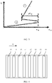
- FIG. 2 shows the three operating modes corresponding to the insulated gate bipolar transistor during operation
- FIG. 3 is a partially enlarged view of A in FIG. 2 , where 1 represents the FRD mode, 2 represents the MOSFET mode, and 3 represents the IGBT mode. It can be seen from FIG. 2 and FIG. 3 that, when power is supplied to both the first metal electrode 15 and the second metal electrode 14, after the gate trench is opened, no electron hole is injected into a back surface of the insulated gate bipolar transistor at a start stage.
- the insulated gate bipolar transistor first operates in the MOSFET mode. After a voltage reaches V SB , the insulated gate bipolar transistor quickly enters the IGBT mode from the MOSFET mode, where the insulated gate bipolar transistor stays in the MOSFET mode for very short time. Because an MCU operates in a light load state most of time, the MCU expects that a switching element (the insulated gate bipolar transistor) of an inverter operates in the MOSFET mode more time. In addition, when the MCU is in full load, the MCU expects that the insulated gate bipolar transistor can quickly switch to the IGBT mode. Therefore, from a perspective of improving MCU efficiency, the MCU expects that an operation mode of the switching element can be more accurately controlled.
- the insulated gate bipolar transistor provided in this embodiment of this application further provides another power supply mode: supplying power to only the first metal electrode 15 or the second metal electrode 14. It can be learned from the foregoing structure of the insulated gate bipolar transistor that, when the structure in which the first metal electrode 15 is electrically connected to only the collector 12, the second metal electrode 14 is electrically connected to only the drain 13, and the first metal electrode 15 is electrically isolated from the second metal electrode 14 is used, the back surface of the insulated gate bipolar transistor is divided into two regions through electrical isolation between the first metal electrode 15 and the second metal electrode 14: an IGBT region and a MOSFET region. During use, power may be separately supplied to the IGBT region and the MOSFET region to control the insulated gate bipolar transistor.
- the insulated gate bipolar transistor can implement the IGBT mode and the MOSFET mode.
- the insulated gate bipolar transistor can implement the FRD mode and the MOSFET mode.
- the MCU can operate in the MOSFET mode for long time.
- the MCU can switch between the MOSFET mode and the IGBT mode.
- the MCU can accurately control the operating mode of the device by using the two metal electrodes on the back surface together with the gate 8. Based on a power output requirement of the MCU, it is determined whether the insulated gate bipolar transistor operates in the MOSFET mode or the IGBT mode. Therefore, a motor can be more accurately controlled.
- a width of the collector 12 is made greater than a width of the drain 13, so that an electron hole can be easily injected from the collector 12. Therefore, a small fast recovery voltage and a small conduction resistance can be implemented.
- a condition for reducing a fast recovery voltage in a current density at a fast recovery peak voltage, a voltage drop needs to be caused for the N buffer layer 11 in the horizontal direction of FIG. 1 , so that a potential difference between a middle point of the collector 12 and the drain 13 becomes greater than or equal to 0.5 V, and preferably, greater than or equal to 0.7 V.
- a larger width of the collector 12 in the first direction a in FIG.
- MOSFET characteristics namely, a relatively small fast recovery voltage and a relatively small conduction resistance are implemented.
- MOSFET operation range can be obtained.
- a larger repetition spacing between the collector 12 and the drain 13 enables a fast recovery voltage to be smaller.
- a repetition spacing between the collector 12 and the drain 13 is greater than or equal to 5 times a repetition spacing between the N-drift layer 1 and the P-drift layer 2 and is less than 20,000 times the repetition spacing between the N-drift layer 1 and the P-drift layer 2.
- the insulated gate bipolar transistor provided in this embodiment of this application may be of a planar gate structure, provided that device characteristics of the IGBT can be implemented.
- FIG. 4 shows another insulated gate bipolar transistor.
- first metal electrodes 15 are in a one-to-one correspondence with the collectors 12
- second metal electrodes 15 are in a one-to-one correspondence with the drains
- any adjacent first metal electrode 15 and second metal electrode 15 are electrically isolated from each other.
- the first metal electrodes 15 and the second metal electrodes 15 are alternately arranged in the first direction a.
- an embodiment of this application further provides a motor control unit.
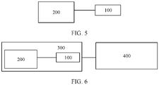
- the motor control unit includes a power module 200 and the insulated gate bipolar transistor 100 that is connected to the power module 200 and that is described in any one of the foregoing embodiments.
- the motor control unit may be configured to control a motor to operate. Because the MCU operates in a light load state most of time, the MCU expects that a switching element (the insulated gate bipolar transistor 100) of an inverter operates in a MOSFET mode more time. In addition, when the MCU is in full load, the MCU expects that the insulated gate bipolar transistor 100 can quickly switch to an IGBT mode.
- a back surface of the insulated gate bipolar transistor 100 is divided into two regions through electrical isolation between the first metal electrode and the second metal electrode: an IGBT region and a MOSFET region.
- power may be separately supplied to the IGBT region and the MOSFET region to control the insulated gate bipolar transistor 100.
- the insulated gate bipolar transistor 100 can implement the IGBT mode and the MOSFET mode.
- the insulated gate bipolar transistor 100 can implement an FRD mode and the MOSFET mode.
- the MCU When the MCU is in light load, power may be supplied to only the second metal electrode. In this case, the MCU can operate in the MOSFET mode for long time. When the MCU is in heavy load, power may be supplied to both the first metal electrode and the second metal electrode. In this case, the MCU can switch between the MOSFET mode and the IGBT mode. It can be learned from the foregoing description that, the MCU can accurately control an operating mode of the device by using the two metal electrodes on the back surface together with the gate. Based on a power output requirement of the MCU, it is determined whether the insulated gate bipolar transistor 100 operates in the MOSFET mode or the IGBT mode. Therefore, the motor can be more accurately controlled.
- the vehicle includes a motor 400 and a motor control unit 300 that is connected to the motor 400 and that is described in any one of the foregoing embodiments.
- the motor control unit 300 may be configured to control the motor 400 to operate. Because the MCU operates in a light load state most of time, the MCU expects that a switching element (the insulated gate bipolar transistor 100) of an inverter operates in a MOSFET mode more time. In addition, when the MCU is in full load, the MCU expects that the insulated gate bipolar transistor 100 can quickly switch to an IGBT mode.
- a back surface of the insulated gate bipolar transistor 100 is divided into two regions through electrical isolation between the first metal electrode and the second metal electrode: an IGBT region and a MOSFET region.
- power may be separately supplied to the IGBT region and the MOSFET region to control the insulated gate bipolar transistor 100.
- the insulated gate bipolar transistor 100 can implement the IGBT mode and the MOSFET mode.
- the insulated gate bipolar transistor 100 can implement an FRD mode and the MOSFET mode.
- the MCU When the MCU is in light load, power may be supplied to only the second metal electrode. In this case, the MCU can operate in the MOSFET mode for long time. When the MCU is in heavy load, power may be supplied to both the first metal electrode and the second metal electrode. In this case, the MCU can switch between the MOSFET mode and the IGBT mode. It can be learned from the foregoing description that, the MCU can accurately control an operating mode of the device by using the two metal electrodes on the back surface together with the gate. Based on a power output requirement of the MCU, it is determined whether the insulated gate bipolar transistor 100 operates in the MOSFET mode or the IGBT mode. Therefore, the motor 400 can be more accurately controlled.
Landscapes
- Metal-Oxide And Bipolar Metal-Oxide Semiconductor Integrated Circuits (AREA)
- Inverter Devices (AREA)
- Insulated Gate Type Field-Effect Transistor (AREA)
Applications Claiming Priority (1)
| Application Number | Priority Date | Filing Date | Title |
|---|---|---|---|
| PCT/CN2020/079555 WO2021184172A1 (zh) | 2020-03-17 | 2020-03-17 | 一种绝缘栅双极型晶体管、电机控制器及汽车 |
Publications (2)
| Publication Number | Publication Date |
|---|---|
| EP4109559A1 true EP4109559A1 (de) | 2022-12-28 |
| EP4109559A4 EP4109559A4 (de) | 2023-04-05 |
Family
ID=77768005
Family Applications (1)
| Application Number | Title | Priority Date | Filing Date |
|---|---|---|---|
| EP20926062.9A Pending EP4109559A4 (de) | 2020-03-17 | 2020-03-17 | Bipolartransistor mit isolierter steuerelektrode, motorsteuereinheit für ein kraftfahrzeug |
Country Status (5)
| Country | Link |
|---|---|
| US (1) | US12513925B2 (de) |
| EP (1) | EP4109559A4 (de) |
| JP (1) | JP7486599B2 (de) |
| CN (1) | CN114402443A (de) |
| WO (1) | WO2021184172A1 (de) |
Families Citing this family (1)
| Publication number | Priority date | Publication date | Assignee | Title |
|---|---|---|---|---|
| DE202026101506U1 (de) | 2025-03-28 | 2026-05-07 | Honda Motor Co., Ltd. | Fahrzeug vom Sattelfahr-Typ |
Family Cites Families (15)
| Publication number | Priority date | Publication date | Assignee | Title |
|---|---|---|---|---|
| JP4815885B2 (ja) | 2005-06-09 | 2011-11-16 | トヨタ自動車株式会社 | 半導体装置の制御方法 |
| JP4678547B2 (ja) | 2007-11-06 | 2011-04-27 | 株式会社デンソー | 半導体装置及びその製造方法 |
| US7911023B2 (en) | 2007-11-06 | 2011-03-22 | Denso Corporation | Semiconductor apparatus including a double-sided electrode element and method for manufacturing the same |
| JP4686580B2 (ja) * | 2008-08-14 | 2011-05-25 | 株式会社東芝 | 電力用半導体装置 |
| JP2010074051A (ja) | 2008-09-22 | 2010-04-02 | Tokyo Electric Power Co Inc:The | パワー半導体素子 |
| JP2012142537A (ja) | 2010-12-16 | 2012-07-26 | Mitsubishi Electric Corp | 絶縁ゲート型バイポーラトランジスタとその製造方法 |
| DE112012006441B4 (de) | 2012-05-29 | 2018-07-12 | Mitsubishi Electric Corporation | Bipolartransistor vom Isolierschichttyp |
| CN103219370A (zh) | 2013-03-11 | 2013-07-24 | 电子科技大学 | 一种具有p浮空层电流栓的rc-igbt |
| JP6648429B2 (ja) * | 2014-10-15 | 2020-02-14 | 富士電機株式会社 | 半導体装置 |
| JP2016149430A (ja) * | 2015-02-12 | 2016-08-18 | 株式会社豊田中央研究所 | 逆導通igbtを備える電子装置 |
| JP6693131B2 (ja) * | 2016-01-12 | 2020-05-13 | 富士電機株式会社 | 半導体装置 |
| DE102016110035B4 (de) * | 2016-05-31 | 2020-09-10 | Infineon Technologies Ag | Elektrische Baugruppe, die eine bipolare Schaltvorrichtung und einen selbstleitenden Transistor mit breiter Bandlücke umfasst, und eine elektrische Baugruppe, die eine bipolare Schaltvorrichtung und einen selbstleitenden Junction-Feldeffekttransistor umfasst, der einen Halbleiterbereich aus Siliziumcarbid umfasst |
| CN107464842A (zh) * | 2017-08-03 | 2017-12-12 | 电子科技大学 | 一种具有集电极槽的超结逆导型igbt |
| CN107768429B (zh) * | 2017-10-27 | 2020-11-13 | 电子科技大学 | 一种具有混合导电模式的超结igbt器件 |
| CN109888005B (zh) | 2019-01-22 | 2021-11-09 | 上海华虹宏力半导体制造有限公司 | 逆导型超结igbt器件及其制造方法 |
-
2020
- 2020-03-17 JP JP2022556190A patent/JP7486599B2/ja active Active
- 2020-03-17 EP EP20926062.9A patent/EP4109559A4/de active Pending
- 2020-03-17 WO PCT/CN2020/079555 patent/WO2021184172A1/zh not_active Ceased
- 2020-03-17 CN CN202080064553.7A patent/CN114402443A/zh active Pending
-
2022
- 2022-09-16 US US17/946,111 patent/US12513925B2/en active Active
Also Published As
| Publication number | Publication date |
|---|---|
| WO2021184172A1 (zh) | 2021-09-23 |
| JP2023518445A (ja) | 2023-05-01 |
| JP7486599B2 (ja) | 2024-05-17 |
| EP4109559A4 (de) | 2023-04-05 |
| US12513925B2 (en) | 2025-12-30 |
| US20230018508A1 (en) | 2023-01-19 |
| CN114402443A (zh) | 2022-04-26 |
Similar Documents
| Publication | Publication Date | Title |
|---|---|---|
| US10872959B2 (en) | Semiconductor device and power converter | |
| JP5875680B2 (ja) | 絶縁ゲート型バイポーラトランジスタ | |
| CN103022089A (zh) | 一种无snapback效应的逆导型绝缘栅双极晶体管 | |
| JPH03238871A (ja) | 半導体装置およびその製造方法 | |
| JPWO2011080928A1 (ja) | 半導体装置、及びそれを用いた電力変換装置 | |
| CN113782592B (zh) | 一种衬底集成反并联续流二极管的rc-ligbt器件 | |
| WO2019085850A1 (zh) | Igbt功率器件 | |
| US20250212434A1 (en) | Semiconductor device and power conversion device | |
| CN106024876A (zh) | 用于消除回滞现象的逆导型横向绝缘栅双极型晶体管器件 | |
| TWI836801B (zh) | 半導體裝置、半導體裝置之製造方法及電力變換裝置 | |
| CN107768434A (zh) | 一种双向igbt及其制造方法 | |
| US12513925B2 (en) | Insulated gate bipolar transistor, motor control unit, and vehicle | |
| JPH04261065A (ja) | 半導体装置 | |
| CN102194864A (zh) | 一种具有体电极的沟槽栅型绝缘栅双极型晶体管 | |
| JP3491049B2 (ja) | 整流素子およびその駆動方法 | |
| CN101330103B (zh) | 绝缘栅型晶体管以及逆变器电路 | |
| US20250311396A1 (en) | Power conversion device, method of controlling power conversion device, semiconductor device, and method of controlling semiconductor device | |
| CN103928507B (zh) | 一种逆导型双栅绝缘栅双极型晶体管 | |
| US20220246720A1 (en) | Superjunction reverse conducting insulated gate bipolar transistor and electric automobile motor control unit | |
| CN107464839B (zh) | 一种防止关断失效的栅控晶闸管器件 | |
| US20250185351A1 (en) | Reverse conducting igbt power device and preparation method therefor, and electronic device | |
| CN102184948A (zh) | 一种改进的平面绝缘栅双极型晶体管 | |
| CN212750900U (zh) | 一种平面型的igbt半导体功率器件 | |
| JP2008300590A (ja) | 双方向横形絶縁ゲート型バイポーラトランジスタ | |
| CN107516671B (zh) | 一种改善关断特性的栅控晶闸管器件 |
Legal Events
| Date | Code | Title | Description |
|---|---|---|---|
| STAA | Information on the status of an ep patent application or granted ep patent |
Free format text: STATUS: THE INTERNATIONAL PUBLICATION HAS BEEN MADE |
|
| PUAI | Public reference made under article 153(3) epc to a published international application that has entered the european phase |
Free format text: ORIGINAL CODE: 0009012 |
|
| STAA | Information on the status of an ep patent application or granted ep patent |
Free format text: STATUS: REQUEST FOR EXAMINATION WAS MADE |
|
| 17P | Request for examination filed |
Effective date: 20220922 |
|
| AK | Designated contracting states |
Kind code of ref document: A1 Designated state(s): AL AT BE BG CH CY CZ DE DK EE ES FI FR GB GR HR HU IE IS IT LI LT LU LV MC MK MT NL NO PL PT RO RS SE SI SK SM TR |
|
| A4 | Supplementary search report drawn up and despatched |
Effective date: 20230309 |
|
| RIC1 | Information provided on ipc code assigned before grant |
Ipc: H01L 29/08 20060101ALN20230302BHEP Ipc: H01L 29/06 20060101ALI20230302BHEP Ipc: H01L 29/739 20060101ALI20230302BHEP Ipc: H01L 29/78 20060101AFI20230302BHEP |
|
| DAV | Request for validation of the european patent (deleted) | ||
| DAX | Request for extension of the european patent (deleted) |