EP4113605A1 - Agencement de module d'alimentation à semi-conducteur - Google Patents
Agencement de module d'alimentation à semi-conducteur Download PDFInfo
- Publication number
- EP4113605A1 EP4113605A1 EP21183453.6A EP21183453A EP4113605A1 EP 4113605 A1 EP4113605 A1 EP 4113605A1 EP 21183453 A EP21183453 A EP 21183453A EP 4113605 A1 EP4113605 A1 EP 4113605A1
- Authority
- EP
- European Patent Office
- Prior art keywords
- semiconductor die
- metallization
- chip
- semiconductor
- chip metallization
- Prior art date
- Legal status (The legal status is an assumption and is not a legal conclusion. Google has not performed a legal analysis and makes no representation as to the accuracy of the status listed.)
- Granted
Links
Images


Classifications
-
- H—ELECTRICITY
- H10—SEMICONDUCTOR DEVICES; ELECTRIC SOLID-STATE DEVICES NOT OTHERWISE PROVIDED FOR
- H10W—GENERIC PACKAGES, INTERCONNECTIONS, CONNECTORS OR OTHER CONSTRUCTIONAL DETAILS OF DEVICES COVERED BY CLASS H10
- H10W40/00—Arrangements for thermal protection or thermal control
- H10W40/20—Arrangements for cooling
- H10W40/25—Arrangements for cooling characterised by their materials
- H10W40/255—Arrangements for cooling characterised by their materials having a laminate or multilayered structure, e.g. direct bond copper [DBC] ceramic substrates
-
- H—ELECTRICITY
- H10—SEMICONDUCTOR DEVICES; ELECTRIC SOLID-STATE DEVICES NOT OTHERWISE PROVIDED FOR
- H10W—GENERIC PACKAGES, INTERCONNECTIONS, CONNECTORS OR OTHER CONSTRUCTIONAL DETAILS OF DEVICES COVERED BY CLASS H10
- H10W20/00—Interconnections in chips, wafers or substrates
- H10W20/40—Interconnections external to wafers or substrates, e.g. back-end-of-line [BEOL] metallisations or vias connecting to gate electrodes
- H10W20/482—Interconnections external to wafers or substrates, e.g. back-end-of-line [BEOL] metallisations or vias connecting to gate electrodes for individual devices provided for in groups H10D8/00 - H10D48/00, e.g. for power transistors
- H10W20/484—Interconnections having extended contours, e.g. pads having mesh shape or interconnections comprising connected parallel stripes
-
- H—ELECTRICITY
- H10—SEMICONDUCTOR DEVICES; ELECTRIC SOLID-STATE DEVICES NOT OTHERWISE PROVIDED FOR
- H10W—GENERIC PACKAGES, INTERCONNECTIONS, CONNECTORS OR OTHER CONSTRUCTIONAL DETAILS OF DEVICES COVERED BY CLASS H10
- H10W90/00—Package configurations
-
- H—ELECTRICITY
- H10—SEMICONDUCTOR DEVICES; ELECTRIC SOLID-STATE DEVICES NOT OTHERWISE PROVIDED FOR
- H10W—GENERIC PACKAGES, INTERCONNECTIONS, CONNECTORS OR OTHER CONSTRUCTIONAL DETAILS OF DEVICES COVERED BY CLASS H10
- H10W90/00—Package configurations
- H10W90/701—Package configurations characterised by the relative positions of pads or connectors relative to package parts
-
- H—ELECTRICITY
- H10—SEMICONDUCTOR DEVICES; ELECTRIC SOLID-STATE DEVICES NOT OTHERWISE PROVIDED FOR
- H10W—GENERIC PACKAGES, INTERCONNECTIONS, CONNECTORS OR OTHER CONSTRUCTIONAL DETAILS OF DEVICES COVERED BY CLASS H10
- H10W70/00—Package substrates; Interposers; Redistribution layers [RDL]
- H10W70/60—Insulating or insulated package substrates; Interposers; Redistribution layers
- H10W70/611—Insulating or insulated package substrates; Interposers; Redistribution layers for connecting multiple chips together
-
- H—ELECTRICITY
- H10—SEMICONDUCTOR DEVICES; ELECTRIC SOLID-STATE DEVICES NOT OTHERWISE PROVIDED FOR
- H10W—GENERIC PACKAGES, INTERCONNECTIONS, CONNECTORS OR OTHER CONSTRUCTIONAL DETAILS OF DEVICES COVERED BY CLASS H10
- H10W70/00—Package substrates; Interposers; Redistribution layers [RDL]
- H10W70/60—Insulating or insulated package substrates; Interposers; Redistribution layers
- H10W70/62—Insulating or insulated package substrates; Interposers; Redistribution layers characterised by their interconnections
- H10W70/65—Shapes or dispositions of interconnections
-
- H—ELECTRICITY
- H10—SEMICONDUCTOR DEVICES; ELECTRIC SOLID-STATE DEVICES NOT OTHERWISE PROVIDED FOR
- H10W—GENERIC PACKAGES, INTERCONNECTIONS, CONNECTORS OR OTHER CONSTRUCTIONAL DETAILS OF DEVICES COVERED BY CLASS H10
- H10W72/00—Interconnections or connectors in packages
- H10W72/071—Connecting or disconnecting
- H10W72/073—Connecting or disconnecting of die-attach connectors
- H10W72/07331—Connecting techniques
-
- H—ELECTRICITY
- H10—SEMICONDUCTOR DEVICES; ELECTRIC SOLID-STATE DEVICES NOT OTHERWISE PROVIDED FOR
- H10W—GENERIC PACKAGES, INTERCONNECTIONS, CONNECTORS OR OTHER CONSTRUCTIONAL DETAILS OF DEVICES COVERED BY CLASS H10
- H10W72/00—Interconnections or connectors in packages
- H10W72/071—Connecting or disconnecting
- H10W72/075—Connecting or disconnecting of bond wires
- H10W72/07521—Aligning
-
- H—ELECTRICITY
- H10—SEMICONDUCTOR DEVICES; ELECTRIC SOLID-STATE DEVICES NOT OTHERWISE PROVIDED FOR
- H10W—GENERIC PACKAGES, INTERCONNECTIONS, CONNECTORS OR OTHER CONSTRUCTIONAL DETAILS OF DEVICES COVERED BY CLASS H10
- H10W72/00—Interconnections or connectors in packages
- H10W72/071—Connecting or disconnecting
- H10W72/075—Connecting or disconnecting of bond wires
- H10W72/07551—Connecting or disconnecting of bond wires characterised by changes in properties of the bond wires during the connecting
- H10W72/07554—Connecting or disconnecting of bond wires characterised by changes in properties of the bond wires during the connecting changes in dispositions
-
- H—ELECTRICITY
- H10—SEMICONDUCTOR DEVICES; ELECTRIC SOLID-STATE DEVICES NOT OTHERWISE PROVIDED FOR
- H10W—GENERIC PACKAGES, INTERCONNECTIONS, CONNECTORS OR OTHER CONSTRUCTIONAL DETAILS OF DEVICES COVERED BY CLASS H10
- H10W72/00—Interconnections or connectors in packages
- H10W72/30—Die-attach connectors
- H10W72/321—Structures or relative sizes of die-attach connectors
- H10W72/325—Die-attach connectors having a filler embedded in a matrix
-
- H—ELECTRICITY
- H10—SEMICONDUCTOR DEVICES; ELECTRIC SOLID-STATE DEVICES NOT OTHERWISE PROVIDED FOR
- H10W—GENERIC PACKAGES, INTERCONNECTIONS, CONNECTORS OR OTHER CONSTRUCTIONAL DETAILS OF DEVICES COVERED BY CLASS H10
- H10W72/00—Interconnections or connectors in packages
- H10W72/30—Die-attach connectors
- H10W72/351—Materials of die-attach connectors
- H10W72/352—Materials of die-attach connectors comprising metals or metalloids, e.g. solders
-
- H—ELECTRICITY
- H10—SEMICONDUCTOR DEVICES; ELECTRIC SOLID-STATE DEVICES NOT OTHERWISE PROVIDED FOR
- H10W—GENERIC PACKAGES, INTERCONNECTIONS, CONNECTORS OR OTHER CONSTRUCTIONAL DETAILS OF DEVICES COVERED BY CLASS H10
- H10W72/00—Interconnections or connectors in packages
- H10W72/30—Die-attach connectors
- H10W72/351—Materials of die-attach connectors
- H10W72/353—Materials of die-attach connectors not comprising solid metals or solid metalloids, e.g. ceramics
- H10W72/354—Materials of die-attach connectors not comprising solid metals or solid metalloids, e.g. ceramics comprising polymers
-
- H—ELECTRICITY
- H10—SEMICONDUCTOR DEVICES; ELECTRIC SOLID-STATE DEVICES NOT OTHERWISE PROVIDED FOR
- H10W—GENERIC PACKAGES, INTERCONNECTIONS, CONNECTORS OR OTHER CONSTRUCTIONAL DETAILS OF DEVICES COVERED BY CLASS H10
- H10W72/00—Interconnections or connectors in packages
- H10W72/50—Bond wires
- H10W72/531—Shapes of wire connectors
- H10W72/533—Cross-sectional shape
- H10W72/534—Cross-sectional shape being rectangular
-
- H—ELECTRICITY
- H10—SEMICONDUCTOR DEVICES; ELECTRIC SOLID-STATE DEVICES NOT OTHERWISE PROVIDED FOR
- H10W—GENERIC PACKAGES, INTERCONNECTIONS, CONNECTORS OR OTHER CONSTRUCTIONAL DETAILS OF DEVICES COVERED BY CLASS H10
- H10W72/00—Interconnections or connectors in packages
- H10W72/50—Bond wires
- H10W72/531—Shapes of wire connectors
- H10W72/5363—Shapes of wire connectors the connected ends being wedge-shaped
-
- H—ELECTRICITY
- H10—SEMICONDUCTOR DEVICES; ELECTRIC SOLID-STATE DEVICES NOT OTHERWISE PROVIDED FOR
- H10W—GENERIC PACKAGES, INTERCONNECTIONS, CONNECTORS OR OTHER CONSTRUCTIONAL DETAILS OF DEVICES COVERED BY CLASS H10
- H10W72/00—Interconnections or connectors in packages
- H10W72/50—Bond wires
- H10W72/541—Dispositions of bond wires
- H10W72/5449—Dispositions of bond wires not being orthogonal to a side surface of the chip, e.g. fan-out arrangements
-
- H—ELECTRICITY
- H10—SEMICONDUCTOR DEVICES; ELECTRIC SOLID-STATE DEVICES NOT OTHERWISE PROVIDED FOR
- H10W—GENERIC PACKAGES, INTERCONNECTIONS, CONNECTORS OR OTHER CONSTRUCTIONAL DETAILS OF DEVICES COVERED BY CLASS H10
- H10W72/00—Interconnections or connectors in packages
- H10W72/50—Bond wires
- H10W72/541—Dispositions of bond wires
- H10W72/547—Dispositions of multiple bond wires
-
- H—ELECTRICITY
- H10—SEMICONDUCTOR DEVICES; ELECTRIC SOLID-STATE DEVICES NOT OTHERWISE PROVIDED FOR
- H10W—GENERIC PACKAGES, INTERCONNECTIONS, CONNECTORS OR OTHER CONSTRUCTIONAL DETAILS OF DEVICES COVERED BY CLASS H10
- H10W72/00—Interconnections or connectors in packages
- H10W72/50—Bond wires
- H10W72/541—Dispositions of bond wires
- H10W72/547—Dispositions of multiple bond wires
- H10W72/5475—Dispositions of multiple bond wires multiple bond wires connected to common bond pads at both ends of the wires
-
- H—ELECTRICITY
- H10—SEMICONDUCTOR DEVICES; ELECTRIC SOLID-STATE DEVICES NOT OTHERWISE PROVIDED FOR
- H10W—GENERIC PACKAGES, INTERCONNECTIONS, CONNECTORS OR OTHER CONSTRUCTIONAL DETAILS OF DEVICES COVERED BY CLASS H10
- H10W72/00—Interconnections or connectors in packages
- H10W72/50—Bond wires
- H10W72/59—Bond pads specially adapted therefor
-
- H—ELECTRICITY
- H10—SEMICONDUCTOR DEVICES; ELECTRIC SOLID-STATE DEVICES NOT OTHERWISE PROVIDED FOR
- H10W—GENERIC PACKAGES, INTERCONNECTIONS, CONNECTORS OR OTHER CONSTRUCTIONAL DETAILS OF DEVICES COVERED BY CLASS H10
- H10W72/00—Interconnections or connectors in packages
- H10W72/851—Dispositions of multiple connectors or interconnections
- H10W72/874—On different surfaces
- H10W72/884—Die-attach connectors and bond wires
-
- H—ELECTRICITY
- H10—SEMICONDUCTOR DEVICES; ELECTRIC SOLID-STATE DEVICES NOT OTHERWISE PROVIDED FOR
- H10W—GENERIC PACKAGES, INTERCONNECTIONS, CONNECTORS OR OTHER CONSTRUCTIONAL DETAILS OF DEVICES COVERED BY CLASS H10
- H10W72/00—Interconnections or connectors in packages
- H10W72/90—Bond pads, in general
- H10W72/921—Structures or relative sizes of bond pads
- H10W72/926—Multiple bond pads having different sizes
-
- H—ELECTRICITY
- H10—SEMICONDUCTOR DEVICES; ELECTRIC SOLID-STATE DEVICES NOT OTHERWISE PROVIDED FOR
- H10W—GENERIC PACKAGES, INTERCONNECTIONS, CONNECTORS OR OTHER CONSTRUCTIONAL DETAILS OF DEVICES COVERED BY CLASS H10
- H10W72/00—Interconnections or connectors in packages
- H10W72/90—Bond pads, in general
- H10W72/931—Shapes of bond pads
- H10W72/932—Plan-view shape, i.e. in top view
-
- H—ELECTRICITY
- H10—SEMICONDUCTOR DEVICES; ELECTRIC SOLID-STATE DEVICES NOT OTHERWISE PROVIDED FOR
- H10W—GENERIC PACKAGES, INTERCONNECTIONS, CONNECTORS OR OTHER CONSTRUCTIONAL DETAILS OF DEVICES COVERED BY CLASS H10
- H10W74/00—Encapsulations, e.g. protective coatings
-
- H—ELECTRICITY
- H10—SEMICONDUCTOR DEVICES; ELECTRIC SOLID-STATE DEVICES NOT OTHERWISE PROVIDED FOR
- H10W—GENERIC PACKAGES, INTERCONNECTIONS, CONNECTORS OR OTHER CONSTRUCTIONAL DETAILS OF DEVICES COVERED BY CLASS H10
- H10W76/00—Containers; Fillings or auxiliary members therefor; Seals
- H10W76/40—Fillings or auxiliary members in containers, e.g. centering rings
- H10W76/42—Fillings
- H10W76/47—Solid or gel fillings
-
- H—ELECTRICITY
- H10—SEMICONDUCTOR DEVICES; ELECTRIC SOLID-STATE DEVICES NOT OTHERWISE PROVIDED FOR
- H10W—GENERIC PACKAGES, INTERCONNECTIONS, CONNECTORS OR OTHER CONSTRUCTIONAL DETAILS OF DEVICES COVERED BY CLASS H10
- H10W90/00—Package configurations
- H10W90/701—Package configurations characterised by the relative positions of pads or connectors relative to package parts
- H10W90/731—Package configurations characterised by the relative positions of pads or connectors relative to package parts of die-attach connectors
- H10W90/734—Package configurations characterised by the relative positions of pads or connectors relative to package parts of die-attach connectors between a chip and a stacked insulating package substrate, interposer or RDL
-
- H—ELECTRICITY
- H10—SEMICONDUCTOR DEVICES; ELECTRIC SOLID-STATE DEVICES NOT OTHERWISE PROVIDED FOR
- H10W—GENERIC PACKAGES, INTERCONNECTIONS, CONNECTORS OR OTHER CONSTRUCTIONAL DETAILS OF DEVICES COVERED BY CLASS H10
- H10W90/00—Package configurations
- H10W90/701—Package configurations characterised by the relative positions of pads or connectors relative to package parts
- H10W90/751—Package configurations characterised by the relative positions of pads or connectors relative to package parts of bond wires
- H10W90/753—Package configurations characterised by the relative positions of pads or connectors relative to package parts of bond wires between laterally-adjacent chips
-
- H—ELECTRICITY
- H10—SEMICONDUCTOR DEVICES; ELECTRIC SOLID-STATE DEVICES NOT OTHERWISE PROVIDED FOR
- H10W—GENERIC PACKAGES, INTERCONNECTIONS, CONNECTORS OR OTHER CONSTRUCTIONAL DETAILS OF DEVICES COVERED BY CLASS H10
- H10W90/00—Package configurations
- H10W90/701—Package configurations characterised by the relative positions of pads or connectors relative to package parts
- H10W90/751—Package configurations characterised by the relative positions of pads or connectors relative to package parts of bond wires
- H10W90/754—Package configurations characterised by the relative positions of pads or connectors relative to package parts of bond wires between a chip and a stacked insulating package substrate, interposer or RDL
Definitions
- the instant disclosure relates to a power semiconductor module arrangement, in particular to a power semiconductor module arrangement comprising at least two switching devices.
- Power semiconductor module arrangements often include at least one semiconductor substrate arranged in a housing.
- a semiconductor arrangement including a plurality of semiconductor elements e.g., two IGBTs or MOSETs in a half-bridge configuration
- Each substrate usually comprises a substrate layer (e.g., a ceramic layer), a first metallization layer deposited on a first side of the substrate layer and (optionally) a second metallization layer deposited on a second side of the substrate layer.
- the semiconductor elements are mounted, for example, on the first metallization layer.
- the second metallization layer may optionally be attached to a base plate.
- the semiconductor devices are usually mounted onto the semiconductor substrate by soldering or sintering techniques.
- the semiconductor elements comprise several chip metallizations, e.g., chip pad metallizations.
- Chip (pad) metallizations of one semiconductor element can be electrically coupled to chip (pad) metallizations of other semiconductor elements or to the first metallization layer by means of electrical connections such as, e.g., bonding wires or ribbons.
- electrical connections are formed using appropriate tools. The tools that are used to form electrical connections, however, may unintentionally damage other structures (e.g., other chip metallizations) formed on the semiconductor elements.
- a power semiconductor module arrangement includes a substrate including a dielectric insulation layer, and a first metallization layer arranged on a first side of the dielectric insulation layer, at least one first semiconductor die implemented as a switching device and mounted on the first metallization layer of the substrate, and at least one second semiconductor die implemented as a switching device and mounted on the first metallization layer of the substrate.
- Each of the at least one first semiconductor die includes a first chip metallization, a second chip metallization and a third chip metallization arranged on a top side of the respective first semiconductor die, wherein a top side of a first semiconductor die is a side of the first semiconductor die that faces away from the substrate, each of the at least one second semiconductor die includes a first chip metallization, a second chip metallization and a third chip metallization arranged on a top side of the respective second semiconductor die, wherein a top side of a second semiconductor die is a side of the second semiconductor die that faces away from the substrate, the first chip metallization, the second chip metallization and the third chip metallization of each of the at least one first semiconductor die form a first pattern on the top side of the respective first semiconductor die, the first chip metallization, the second chip metallization and the third chip metallization of each of the at least one second semiconductor die form a second pattern on the top side of the respective second semiconductor die, the second pattern being different from the first pattern, and the
- An electrical line or electrical connection as described herein may be a single electrically conductive element, or include at least two individual electrically conductive elements connected in series and/or parallel. Electrical lines and electrical connections may include metal and/or semiconductor material, and may be permanently electrically conductive (i.e., non-switchable).
- a semiconductor die has electrically connectable pads and includes at least one semiconductor element with electrodes.
- the power semiconductor module arrangement 100 includes a housing 7 and a substrate 10.
- the substrate 10 includes a dielectric insulation layer 11, a (structured) first metallization layer 111 attached to the dielectric insulation layer 11, and a (structured) second metallization layer 112 attached to the dielectric insulation layer 11.
- the dielectric insulation layer 11 is disposed between the first and second metallization layers 111, 112.
- Each of the first and second metallization layers 111, 112 may consist of or include one of the following materials: copper; a copper alloy; aluminum; an aluminum alloy; any other metal or alloy that remains solid during the operation of the power semiconductor module arrangement.
- the substrate 10 may be a ceramic substrate, that is, a substrate in which the dielectric insulation layer 11 is a ceramic, e.g., a thin ceramic layer.
- the ceramic may consist of or include one of the following materials: aluminum oxide; aluminum nitride; zirconium oxide; silicon nitride; boron nitride; or any other dielectric ceramic.
- the dielectric insulation layer 11 may consist of an organic compound and include one or more of the following materials: Al 2 O 3 , AlN, SiC, BeO, BN, or Si 3 N 4 .
- the substrate 10 may, e.g., be a Direct Copper Bonding (DCB) substrate, a Direct Aluminum Bonding (DAB) substrate, or an Active Metal Brazing (AMB) substrate.
- the substrate 10 may be an Insulated Metal Substrate (IMS).
- An Insulated Metal Substrate generally comprises a dielectric insulation layer 11 comprising (filled) materials such as epoxy resin or polyimide, for example.
- the material of the dielectric insulation layer 11 may be filled with ceramic particles, for example.
- Such particles may comprise, e.g., SiO 2 , Al 2 O 3 , AlN, SiN or BN and may have a diameter of between about 1 ⁇ m and about 50 ⁇ m.
- the substrate 10 may also be a conventional printed circuit board (PCB) having a non-ceramic dielectric insulation layer 11.
- a non-ceramic dielectric insulation layer 11 may consist of or include a cured resin.
- the substrate 10 is arranged in a housing 7.
- the substrate 10 forms a base surface of the housing 7, while the housing 7 itself solely comprises sidewalls and a cover. This, however, is only an example. It is also possible that the housing 7 further comprises a base surface and the substrate 10 is arranged on the base surface inside the housing 7. According to another example (not specifically illustrated), the substrate 10 may be mounted on a base plate. The base plate may form a bottom of the housing 7. In some power semiconductor module arrangements 100, more than one substrate 10 is arranged within the same housing 7.
- One or more semiconductor dies 20 may be arranged on the at least one substrate 10.
- Each of the semiconductor dies 20 arranged on the at least one substrate 10 may include a diode, an IGBT (Insulated-Gate Bipolar Transistor), a MOSFET (Metal-Oxide-Semiconductor Field-Effect Transistor), a JFET (Junction Field-Effect Transistor), a HEMT (High-Electron-Mobility Transistor), or any other suitable semiconductor element.
- IGBT Insulated-Gate Bipolar Transistor
- MOSFET Metal-Oxide-Semiconductor Field-Effect Transistor
- JFET Joint Field-Effect Transistor
- HEMT High-Electron-Mobility Transistor
- the one or more semiconductor dies 20 may form a semiconductor arrangement on the substrate 10.
- the second metallization layer 112 of the substrate 10 in Figure 1 is a continuous layer.
- the second metallization layer 112 may be a structured layer.
- the second metallization layer 112 may be omitted.
- the first metallization layer 111 is a structured layer in the example illustrated in Figure 1 .
- "Structured layer" in this context means that the respective metallization layer is not a continuous layer, but includes recesses between different sections of the layer. Such recesses are schematically illustrated in Figure 1 .
- the first metallization layer 111 in this example includes three different sections.
- Different semiconductor dies 20 may be mounted to the same or to different sections of the first metallization layer 111. Different sections of the first metallization layer may have no electrical connection or may be electrically connected to one or more other sections using electrical connections 3 such as, e.g., bonding wires. Semiconductor dies 20 may be electrically connected to each other or to the first metallization layer 111 using electrical connections 3, for example. Electrical connections 3, instead of bonding wires, may also include bonding ribbons, connection plates or conductor rails, for example, to name just a few examples.
- the one or more semiconductor dies 20 may be electrically and mechanically connected to the substrate 10 by an electrically conductive connection layer 60. Such an electrically conductive connection layer 60 may be a solder layer, a layer of an electrically conductive adhesive, or a layer of a sintered metal powder, e.g., a sintered silver (Ag) powder, for example.
- the power semiconductor module arrangement 100 illustrated in Figure 1 further includes terminal elements 4.
- the terminal elements 4 are electrically connected to the first metallization layer 111 and provide an electrical connection between the inside and the outside of the housing 7.
- the terminal elements 4 may be electrically connected to the first metallization layer 111 with a first end, while a second end 41 of the terminal elements 4 protrudes out of the housing 7.
- the terminal elements 4 may be electrically contacted from the outside at their second end 41.
- Such terminal elements 4, however, are only an example.
- the components inside the housing 7 may be electrically contacted from outside the housing 7 in any other suitable way.
- terminal elements 4 may be arranged closer to or adjacent to the sidewalls of the housing 7. It is also possible that terminal elements 4 protrude vertically or horizontally through the sidewalls of the housing 7.
- the first end of a terminal element 4 may be electrically and mechanically connected to the substrate 10 by an electrically conductive connection layer, for example (not explicitly illustrated in Figure 1 ).
- an electrically conductive connection layer may be a solder layer, a layer of an electrically conductive adhesive, or a layer of a sintered metal powder, e.g., a sintered silver (Ag) powder, for example.
- the first end of a terminal element 4 may also be electrically coupled to the substrate 10 via one or more electrical connections 3, for example.
- the power semiconductor module arrangement 100 generally further includes an encapsulant 5.
- the encapsulant 5 may consist of or include a silicone gel or may be a rigid molding compound, for example.
- the encapsulant 5 may at least partly fill the interior of the housing 7, thereby covering the components and electrical connections that are arranged on the substrate 10.
- the terminal elements 4 may be partly embedded in the encapsulant 5. At least their second ends 41, however, are not covered by the encapsulant 5 and protrude from the encapsulant 5 through the housing 7 to the outside of the housing 7.
- the encapsulant 5 is configured to protect the components and electrical connections of the power semiconductor module 100, in particular the components arranged inside the housing 7, from certain environmental conditions and mechanical damage. It is generally also possible to omit the housing 7 and solely protect the substrate 10 and any components mounted thereon with an encapsulant 5.
- the encapsulant 5 may be a rigid material, for example.
- the power semiconductor module arrangement 200 comprises a substrate 10, similar to the substrate 10 that has been described with respect to Figure 1 above.
- the first metallization layer 111 in the example of Figure 2 comprises a plurality x of different sections 111 x .
- a plurality of semiconductor dies 22, 24, 26 is arranged on the substrate 10.
- Three first semiconductor dies 24 are arranged on one section 111 1 of the first metallization layer 111, three second semiconductor dies 26 are arranged on another section 111 7 of the first metallization layer 111, and a plurality of third semiconductor dies 22 are arranged on even further sections of the first metallization layer 111.
- the first semiconductor dies 24 each include a switching device
- the second semiconductor dies 26 each include a switching device
- the third semiconductor dies 22 each include a diode in the example of Figure 2 .
- the first semiconductor dies 24 form high side switches
- the second semiconductor dies 26 form low side switches. That is, the first semiconductor dies 24 each include a load path between a first load terminal and a second load terminal, and a control terminal
- the second semiconductor dies 26 each include a load path between a first load terminal and a second load terminal and a control terminal.
- the first load terminals of the first semiconductor dies 24 are coupled to a first potential (e.g., positive potential), the second load terminals of the first semiconductor dies 24 are coupled to the first load terminals of the second semiconductor dies 26, and the second load terminals of the second semiconductor dies 26 are coupled to a second potential (e.g., negative potential or ground).
- the first semiconductor dies 24 and the second semiconductor dies 26 in this example are arranged in a half-bridge configuration.
- the third semiconductor dies 22 form rectifier diodes, for example.
- a plurality of terminal elements 4 is also mounted on different sections of the first metallization layer 111.
- the different semiconductor dies 22, 24, 26 are electrically coupled to each other or to different sections of the first metallization layer 111 by means of electrical connections 3, as has been described above.
- the plurality of first semiconductor dies 24, the plurality of second semiconductor dies 26 and the plurality of third semiconductor dies 22 form a three-phase power inverter.
- the first semiconductor dies 24 and the second semiconductor dies 26 are often implemented identically with regard to the size and position of different chip (pad) metallizations. Exemplary chip (pad) metallizations will be described further below.
- a power semiconductor module arrangement 200 comprising three first semiconductor dies 24 and three second semiconductor dies 26 is only any example.
- the power semiconductor module arrangement 200 generally can comprise any number of first semiconductor dies 24 and second semiconductor dies 26. According to one example, the number of first semiconductor dies 24 equals the number of second semiconductor dies 26.
- the power semiconductor module arrangement 200 may also include any suitable number of third semiconductor dies 22 and, optionally, any other semiconductor devices.
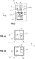
- This section A includes part of a first section 111 1 of the first metallization layer 111, a second section 111 2 of the first metallization layer 111, and a third section 111 3 of the first metallization layer 111.
- a first semiconductor die 24 is mounted on the first section 111 1 and terminal elements 4 are mounted on each of the second section 111 2 and the third section 111 3 .
- the first semiconductor die 24 comprises a first chip (pad) metallization 24 1 , a second chip (pad) metallization 24 2 and a third chip metallization 24 3 , arranged on a top side of the first semiconductor die 24.
- the top side of the first semiconductor die 24 is a side of the first semiconductor die 24 which faces away from the substrate 10.
- IGBT Insulated-Gate Bipolar Transistor
- MOSFET Metal-Oxide-Semiconductor Field-Effect Transistor
- JFET Joint Field-Effect Transistor
- HEMT High-Electron-Mobility Transistor
- the first load terminal of the first semiconductor die 24 may be connected to a further chip (pad) metallization (not visible in Figure 3 ) formed on a bottom side of the first semiconductor die 24, and mechanically and electrically coupled to the first section 111 1 .
- the second load terminal of the first semiconductor die 24 may be connected to the first chip (pad) metallization 24 1
- the control terminal of the first semiconductor die 24 may be connected to the second chip (pad) metallization 24 2 .
- the first chip (pad) metallization 24 1 is electrically coupled to the second section 111 2 of the first metallization layer 111 by means of electrical connections 3 (e.g., bonding wires).
- the second section 1112 can be electrically contacted from the outside of the power semiconductor module arrangement 200 by means of terminal element 4.
- the second chip (pad) metallization 24 2 is electrically coupled to the third section 111 3 by means of another electrical connection 3.
- the third section 111 3 can be electrically contacted from the outside of the power semiconductor module arrangement 200 by means of terminal element 4.
- the first chip (pad) metallization 24 1 and the second chip (pad) metallization 24 2 are extensive metallizations that have a square or rectangular cross-section, for example, in order to provide an area that is large enough to form a connection to one or more electrical connections 3.
- the third chip metallization 24 3 is an elongated metallization extending along the edges of the first semiconductor die 24.
- the third chip metallization 24 3 may form a termination field plate electrode, for example. Such termination field plates are often used in order to spread the electric fields occurring during the use of the first semiconductor die 24 more uniformly in the edge regions. In this way, the breakdown voltage of the device can be increased.
- the third chip metallization 24 3 is covered by a thin layer of imide.
- the electrical connections 3 are formed using appropriate tools.
- the tools that are used to form electrical connections 3, however, may unintentionally damage other structures (e.g., other chip metallizations) formed on the semiconductor elements.
- a tool may scratch the surface of the first semiconductor die 24 close to the second chip (pad) metallization 24 2 , after forming a mechanical connection between the electrical connection 3 and the second chip (pad) metallization 24 2 .
- the electrical connection 3 is first mounted to the third section 111 3 with a first end, and is subsequently mounted to the first semiconductor die 24 with a second end. This direction is chosen, because the terminal element 4 restricts the movement of the tool in the other direction.
- the mounting direction is indicated by the arrow in Figure 3 .
- the electrical connection 3 is usually cut from a continuous wire or ribbon.
- the wire or ribbon may be cut after securely attaching the second end of the electrical connection 3.
- the tool usually cannot be immediately lifted from the first semiconductor die 24, but instead moves further close to the top surface of the respective first semiconductor die 24 for a certain distance.
- the tool may already have lifted off the first semiconductor die 24 far enough by the time it crosses the third chip metallization 24 3 , in order to prevent it from scratching and thereby damaging the third chip metallization 24 3 . Similar problems may arise concerning the other ones of the first semiconductor dies 24 as well as the second semiconductor dies 26 (see, e.g., section B as indicated in Figure 2 ).
- the layout of the chip metallizations on a top surface of the semiconductor dies 24, 26 therefore may be chosen in such a way that damages of any (metallic) structures on a top surface of the semiconductor dies 24, 26 by means of any tools that are used to form electrical connections 3 can be reduced or even avoided. According to one example, it is possible to use one and the same layout for as many semiconductor dies 24, 26 as possible, instead of designing individual layouts for each of the different semiconductor dies 24, 26.
- the first chip metallization 24 1 , the second chip metallization 24 2 and the third chip metallization 24 3 of the first semiconductor dies 24 of a power semiconductor module arrangement 200 form a first pattern
- the first chip metallization 26 1 , the second chip metallization 26 2 and the third chip metallization 26 3 of the second semiconductor dies 26 of a power semiconductor module arrangement 200 form a second pattern, the second pattern being different from the first pattern.
- Figure 4A schematically illustrates a second semiconductor die 26
- Figure 4B schematically illustrates a first semiconductor die 24.
- the first semiconductor die 24 in this example has a square cross-section, but may also have a rectangular cross-section instead.
- the third chip metallization 24 3 is a circumferential metallization that extends continuously along all of the four edges of the first semiconductor die 24.
- the first chip metallization 24 1 has a rectangular cross-section and extends between a first side 1 24 of the first semiconductor die 24 and a second side 2 24 of the first semiconductor die 24, opposite the first side 1 24 .
- the first chip metallization 24 1 is arranged closer to a third side 3 24 of the first semiconductor die 24 than to a fourth side 4 24 of the first semiconductor die 24, opposite the third side 3 24 .
- the first chip metallization 24 1 therefore, may be arranged on one half of the first semiconductor die 24.
- the second chip metallization 24 2 is arranged on the second half of the first semiconductor die 24.
- the second chip metallization 24 2 also has a rectangular cross-section, extends between the first side 1 24 and the second side 2 24 , and is arranged closer to the fourth side 4 24 than to the third side 3 24 .
- the second chip metallization 24 2 has a smaller cross-section than the first chip metallization 24 1 and is arranged closer to the first side 1 24 than to the second side 2 24 .
- a length of the second chip metallization 24 2 in a horizontal direction y perpendicular to the first side 1 24 and the second side 2 24 is shorter than a length of the first chip metallization 24 1 in the same direction y.
- a corner formed between the second side 2 24 and the fourth side 4 24 inside of the third chip metallization 24 3 is not covered by either the first chip metallization 24 1 or the second chip metallization 24 2 or by any other metallization.
- an electrical connection 3 is formed such that it ends on the first semiconductor chip 24 (e.g., on the second chip metallization 24 2 ), as has been described with respect to Figure 3 above, the area in this corner in which no metallization is formed functions as a lift-off area for the (bonding) tool. Damages to the third chip metallization 24 3 can be avoided or at least reduced in this way.
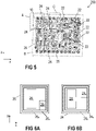
- the first semiconductor die 24 When the first semiconductor die 24 is mirrored along an axis of symmetry Y, this results in the second semiconductor die 26 (see Figure 5A ). That is, the first pattern of the first semiconductor die 24 is mirror symmetric with the second pattern of the second semiconductor die 26.
- the first pattern and the second pattern are not superimposable. This means that the first pattern and the second pattern cannot be exactly aligned with each other.
- the first pattern and the second pattern therefore are chiral patterns.
- the first semiconductor dies 24 in this example comprise the first, second and third chip metallizations 24i, 24 2 , 24 3 arranged in the first pattern
- the second semiconductor dies 26 comprise the first, second and third chip metallizations 26i, 26 2 , 26 3 arranged in the second pattern as have been described with respect to Figure 4 above.
- the first semiconductor dies 24 and the second semiconductor dies 26 of the power semiconductor module arrangement 200 therefore, are realized using only two different patterns. Generally, however, it is also possible to realize one or more of the first and/or second semiconductor dies 24, 26 using even further (chiral) patterns. In order to keep the design of the power semiconductor module arrangement 200 as simple and cost-effective as possible, however, as few different patterns as possible may be used.
- the distance d1 between the second chip metallization 24 2 , 26 2 and the respective third chip metallization 24 3 , 26 3 in a direction of movement of a (bonding) tool is still large enough, even if an overall size of the first and second semiconductor dies 24, 26 is further reduced.
- a transistor device generally comprises a plurality of individual transistor cells formed in the semiconductor body of the transistor device. Each individual transistor cell usually comprises a gate electrode.
- a gate runner 24 4 , 26 4 electrically couples the plurality of gate electrodes to the gate pad (e.g., second chip metallization 24 2 , 26 2 ).
- the gate runner 24 4 , 26 4 may be a circumferential metallization region extending along the four different sides of the respective semiconductor die 24, 26.
- the third chip metallization 24 3 , 26 3 is arranged between the gate runner 24 4 , 26 4 and the edges of the respective semiconductor die 24, 26.
- FIG. 7 and 8 it is further possible to form at least one so-called gate finger 24 42 , 26 42 on a top surface of the first and second semiconductor dies 24, 26.
- a gate finger 24 42 , 26 42 may be configured to more uniformly distribute a gate signal to the individual transistor cells of the semiconductor die 24, 26.
- a gate finger 24 42 , 26 42 may continuously extend between two opposite sides of an essentially square or rectangular gate runner 24 4 , 26 4 , as is illustrated in Figures 7A and 7B .
- the gate finger 24 42 , 26 42 may contact only one side of the gate runner 24 4 , 26 4 , but not the opposite side of the 24 4 , 26 4 . This is schematically illustrated in Figures 8A and 8B .
- the gate finger 24 4 , 26 4 may extend centrally on the top surface of the semiconductor die 24, 26 such that one half of the semiconductor die 24, 26 is arranged on one side of the gate finger 24 4 , 26 4 , and another half of the semiconductor die 24, 26 is arranged on the other side of the gate finger 24 4 , 26 4 .
- One or more gate fingers may be arranged in any suitable positions on the top surface of the semiconductor dies 24, 26.
- a power semiconductor module arrangement 200 may comprise at least one first semiconductor die 24 implemented as a switching device and mounted on the first metallization layer 111 of a substrate 10, and at least one second semiconductor die 26 implemented as a switching device and mounted on the first metallization layer 111 of the substrate 10.
- Each of the at least one first semiconductor die 24 comprises a first chip metallization 24 1 , a second chip metallization 24 2 and a third chip metallization 24 3 arranged on a top side of the respective first semiconductor die 24, wherein a top side of a first semiconductor die 24 is a side of the first semiconductor die 24 that faces away from the substrate 10.
- Each of the at least one second semiconductor die 26 comprises a first chip metallization 26 1 , a second chip metallization 26 2 and a third chip metallization 26 3 arranged on a top side of the respective second semiconductor die 26, wherein a top side of a second semiconductor die 26 is a side of the second semiconductor die 26 that faces away from the substrate 10.
- the first chip metallization 24 1 , the second chip metallization 24 2 and the third chip metallization 24 3 of at least one of the at least one first semiconductor die 24 are arranged on the top side of the respective first semiconductor die 24 forming a first pattern
- the first chip metallization 26 1 , the second chip metallization 26 2 and the third chip metallization 26 3 of each of the at least one second semiconductor die 26 are arranged on the top side of the respective second semiconductor die 26 forming a second pattern, wherein the first pattern and the second pattern are chiral patterns.
Landscapes
- Semiconductor Integrated Circuits (AREA)
Priority Applications (1)
| Application Number | Priority Date | Filing Date | Title |
|---|---|---|---|
| EP21183453.6A EP4113605B1 (fr) | 2021-07-02 | 2021-07-02 | Agencement de module d'alimentation à semi-conducteur |
Applications Claiming Priority (1)
| Application Number | Priority Date | Filing Date | Title |
|---|---|---|---|
| EP21183453.6A EP4113605B1 (fr) | 2021-07-02 | 2021-07-02 | Agencement de module d'alimentation à semi-conducteur |
Publications (2)
| Publication Number | Publication Date |
|---|---|
| EP4113605A1 true EP4113605A1 (fr) | 2023-01-04 |
| EP4113605B1 EP4113605B1 (fr) | 2026-04-08 |
Family
ID=76796907
Family Applications (1)
| Application Number | Title | Priority Date | Filing Date |
|---|---|---|---|
| EP21183453.6A Active EP4113605B1 (fr) | 2021-07-02 | 2021-07-02 | Agencement de module d'alimentation à semi-conducteur |
Country Status (1)
| Country | Link |
|---|---|
| EP (1) | EP4113605B1 (fr) |
Citations (5)
| Publication number | Priority date | Publication date | Assignee | Title |
|---|---|---|---|---|
| US20120175688A1 (en) * | 2011-01-10 | 2012-07-12 | International Rectifier Corporation | Semiconductor Package with Reduced On-Resistance and Top Metal Spreading Resistance with Application to Power Transistor Packaging |
| US8294208B2 (en) * | 2008-03-04 | 2012-10-23 | International Rectifier Corporation | Semiconductor device having a gate contact on one surface electrically connected to a gate bus on an opposing surface |
| EP3324434A1 (fr) * | 2016-11-17 | 2018-05-23 | Infineon Technologies AG | Ensemble semi-conducteur comprenant un socle de liaison et procédé de fonctionnement d'un tel ensemble semi-conducteur |
| US20190109225A1 (en) * | 2017-10-10 | 2019-04-11 | Stmicroelectronics S.R.L. | Power mosfet device and manufacturing process thereof |
| US10727209B2 (en) * | 2017-07-25 | 2020-07-28 | Kabushiki Kaisha Toshiba | Semiconductor device and semiconductor element with improved yield |
-
2021
- 2021-07-02 EP EP21183453.6A patent/EP4113605B1/fr active Active
Patent Citations (5)
| Publication number | Priority date | Publication date | Assignee | Title |
|---|---|---|---|---|
| US8294208B2 (en) * | 2008-03-04 | 2012-10-23 | International Rectifier Corporation | Semiconductor device having a gate contact on one surface electrically connected to a gate bus on an opposing surface |
| US20120175688A1 (en) * | 2011-01-10 | 2012-07-12 | International Rectifier Corporation | Semiconductor Package with Reduced On-Resistance and Top Metal Spreading Resistance with Application to Power Transistor Packaging |
| EP3324434A1 (fr) * | 2016-11-17 | 2018-05-23 | Infineon Technologies AG | Ensemble semi-conducteur comprenant un socle de liaison et procédé de fonctionnement d'un tel ensemble semi-conducteur |
| US10727209B2 (en) * | 2017-07-25 | 2020-07-28 | Kabushiki Kaisha Toshiba | Semiconductor device and semiconductor element with improved yield |
| US20190109225A1 (en) * | 2017-10-10 | 2019-04-11 | Stmicroelectronics S.R.L. | Power mosfet device and manufacturing process thereof |
Also Published As
| Publication number | Publication date |
|---|---|
| EP4113605B1 (fr) | 2026-04-08 |
Similar Documents
| Publication | Publication Date | Title |
|---|---|---|
| US12094793B2 (en) | Package with electrically insulated carrier and at least one step on encapsulant | |
| US11239132B2 (en) | Semiconductor power device with corresponding package and related manufacturing process | |
| US12224218B2 (en) | Semiconductor packages with increased power handling | |
| CN109997223B (zh) | 功率半导体模块 | |
| US11942449B2 (en) | Semiconductor arrangement and method for producing the same | |
| EP2889902B1 (fr) | Dispositif électrique à semi-conducteur de puissance | |
| US12387987B2 (en) | Housing, semiconductor module comprising a housing and method for producing a housing | |
| US10410996B2 (en) | Integrated circuit package for assembling various dice in a single IC package | |
| CN110911388A (zh) | 半导体装置 | |
| EP3736858A1 (fr) | Agencement de module semi-conducteur de puissance | |
| US11538725B2 (en) | Semiconductor module arrangement | |
| US11282774B2 (en) | Power semiconductor module arrangement | |
| US11127714B2 (en) | Printed board and semiconductor device | |
| EP4113605B1 (fr) | Agencement de module d'alimentation à semi-conducteur | |
| US20230170286A1 (en) | Terminal Element or Bus Bar, and Power Semiconductor Module Arrangement Comprising a Terminal Element or Bus Bar | |
| EP4421868B1 (fr) | Agencement de module semi-conducteur | |
| EP4607584A1 (fr) | Agencement de module semi-conducteur | |
| US12002740B2 (en) | Printed circuit board, power semiconductor module arrangement comprising a printed circuit board, and method for assembling the same | |
| EP4439649A1 (fr) | Agencement de substrat | |
| US20230420329A1 (en) | Top side cooled semiconductor packages | |
| US20260053010A1 (en) | Power semiconductor module arrangement | |
| EP4601424A1 (fr) | Agencement de module semi-conducteur de puissance | |
| US20260047494A1 (en) | Semiconductor module arrangement | |
| EP4345884A1 (fr) | Ensemble de modules semi-conducteurs de puissance et carte de circuit imprimé pour un ensemble de modules semi-conducteurs de puissance | |
| US20240363497A1 (en) | Semiconductor module arrangements |
Legal Events
| Date | Code | Title | Description |
|---|---|---|---|
| PUAI | Public reference made under article 153(3) epc to a published international application that has entered the european phase |
Free format text: ORIGINAL CODE: 0009012 |
|
| STAA | Information on the status of an ep patent application or granted ep patent |
Free format text: STATUS: REQUEST FOR EXAMINATION WAS MADE |
|
| 17P | Request for examination filed |
Effective date: 20220825 |
|
| AK | Designated contracting states |
Kind code of ref document: A1 Designated state(s): AL AT BE BG CH CY CZ DE DK EE ES FI FR GB GR HR HU IE IS IT LI LT LU LV MC MK MT NL NO PL PT RO RS SE SI SK SM TR |
|
| GRAP | Despatch of communication of intention to grant a patent |
Free format text: ORIGINAL CODE: EPIDOSNIGR1 |
|
| STAA | Information on the status of an ep patent application or granted ep patent |
Free format text: STATUS: GRANT OF PATENT IS INTENDED |
|
| RIC1 | Information provided on ipc code assigned before grant |
Ipc: H01L 25/07 20060101AFI20251107BHEP Ipc: H01L 23/00 20060101ALI20251107BHEP Ipc: H01L 23/482 20060101ALI20251107BHEP Ipc: H01L 23/373 20060101ALN20251107BHEP |
|
| RIC1 | Information provided on ipc code assigned before grant |
Ipc: H01L 25/07 20060101AFI20251114BHEP Ipc: H01L 23/00 20060101ALI20251114BHEP Ipc: H01L 23/482 20060101ALI20251114BHEP Ipc: H01L 23/373 20060101ALN20251114BHEP |
|
| INTG | Intention to grant announced |
Effective date: 20251128 |
|
| GRAS | Grant fee paid |
Free format text: ORIGINAL CODE: EPIDOSNIGR3 |
|
| GRAA | (expected) grant |
Free format text: ORIGINAL CODE: 0009210 |
|
| STAA | Information on the status of an ep patent application or granted ep patent |
Free format text: STATUS: THE PATENT HAS BEEN GRANTED |
|
| AK | Designated contracting states |
Kind code of ref document: B1 Designated state(s): AL AT BE BG CH CY CZ DE DK EE ES FI FR GB GR HR HU IE IS IT LI LT LU LV MC MK MT NL NO PL PT RO RS SE SI SK SM TR |
|
| REG | Reference to a national code |
Ref country code: CH Ref legal event code: F10 Free format text: ST27 STATUS EVENT CODE: U-0-0-F10-F00 (AS PROVIDED BY THE NATIONAL OFFICE) Effective date: 20260408 Ref country code: GB Ref legal event code: FG4D |
|
| REG | Reference to a national code |
Ref country code: DE Ref legal event code: R096 Ref document number: 602021051504 Country of ref document: DE |