EP4113737B1 - Bidirektionaler dielektrischer hochfrequenz(hf)-koppler mit leistungsteiler/combiner-funktion - Google Patents
Bidirektionaler dielektrischer hochfrequenz(hf)-koppler mit leistungsteiler/combiner-funktion Download PDFInfo
- Publication number
- EP4113737B1 EP4113737B1 EP21382573.0A EP21382573A EP4113737B1 EP 4113737 B1 EP4113737 B1 EP 4113737B1 EP 21382573 A EP21382573 A EP 21382573A EP 4113737 B1 EP4113737 B1 EP 4113737B1
- Authority
- EP
- European Patent Office
- Prior art keywords
- tsa
- ultra
- wideband
- bidirectional coupler
- structures
- Prior art date
- Legal status (The legal status is an assumption and is not a legal conclusion. Google has not performed a legal analysis and makes no representation as to the accuracy of the status listed.)
- Active
Links
Images





Classifications
-
- H—ELECTRICITY
- H01—ELECTRIC ELEMENTS
- H01P—WAVEGUIDES; RESONATORS, LINES, OR OTHER DEVICES OF THE WAVEGUIDE TYPE
- H01P5/00—Coupling devices of the waveguide type
- H01P5/12—Coupling devices having more than two ports
- H01P5/16—Conjugate devices, i.e. devices having at least one port decoupled from one other port
- H01P5/18—Conjugate devices, i.e. devices having at least one port decoupled from one other port consisting of two coupled guides, e.g. directional couplers
- H01P5/188—Conjugate devices, i.e. devices having at least one port decoupled from one other port consisting of two coupled guides, e.g. directional couplers the guides being dielectric waveguides
-
- H—ELECTRICITY
- H01—ELECTRIC ELEMENTS
- H01P—WAVEGUIDES; RESONATORS, LINES, OR OTHER DEVICES OF THE WAVEGUIDE TYPE
- H01P5/00—Coupling devices of the waveguide type
- H01P5/08—Coupling devices of the waveguide type for linking dissimilar lines or devices
- H01P5/087—Transitions to a dielectric waveguide
-
- H—ELECTRICITY
- H01—ELECTRIC ELEMENTS
- H01Q—ANTENNAS, i.e. RADIO AERIALS
- H01Q5/00—Arrangements for simultaneous operation of antennas on two or more different wavebands, e.g. dual-band or multi-band arrangements
- H01Q5/20—Arrangements for simultaneous operation of antennas on two or more different wavebands, e.g. dual-band or multi-band arrangements characterised by the operating wavebands
- H01Q5/25—Ultra-wideband [UWB] systems, e.g. multiple resonance systems; Pulse systems
Definitions
- the present invention relates generally to radiofrequency bidirectional couplers with power divider/combiner functionality, a kind of devices used in the field of radio frequency engineering that split the energy of a radio-frequency signal propagating through one of the M input among a group of N outputs (divider), which also enables to combine the energy propagating through various inputs into a common output (combiner).
- This invention discloses a directional coupler structure based on dielectric waveguides that is wideband and broadband. Wideband since it operates over a wide frequency range, and broadband, since is suited for modulated signals occupying a wide bandwidth.
- Radiofrequency (RF) systems operate handling signals in the form of guided electromagnetic waves with frequencies starting around 30 MHz and going up into the millimeter (30 GHz to 300 GHz) and Terahertz (300 GHz to 3000 GHz) regions of the spectrum.
- RF systems might need to split a radiofrequency signal propagating through a waveguide into several copies of itself, with varying amount (split ratio) of energy within each copy, each delivered at different output waveguides. This function constitutes a power divider.
- the reciprocal function combining different RF signals into a common output which constitutes a power combiner, is also of interest.
- bidirectional couplers passive devices known as bidirectional couplers, which are schematically represented in Figure 1 .
- This figure shows a bidirectional coupler (100) with four access ports.
- the incoming signal arrives to the directional coupler at its input port (P1), coupling a defined amount of energy from this input port to an output transmission port (P2) and another amount to a second output, known as coupled port (P4).
- the incoming signal power at the input port (P1) is commonly split between the output ports using transmission lines close to each other, allowing the energy passing through one waveguide to couple into the other by evanescent wave leakage.
- any reflection of the signal exiting through the output port (P2) returning to the device enters at this port (P2), being routed to the isolation port (P3).
- the device is bidirectional as any port can be the input, which will result in the directly connected port being the transmitted port, adjacent port being the isolated port, and the diagonal port being the coupled port.
- Directional couplers and power dividers have many applications. These include providing a signal sample for measurement or monitoring, feedback, combining feeds to and from antennas, antenna beam forming, providing taps for cable distributed systems such as cable TV, and separating transmitted and received signals on telephone lines.
- directional couplers are the documents US 2 794 959 A (FOX ARTHUR G ), US 3 558 213 A (MARCATILI ENRIQUE A J ) and JP 2000 022412 A (KYOCERA CORP ).
- the present invention proposes a new bidirectional coupler with power divider/combiner functionality based on dielectric waveguide structures to extend the operation frequency range of the device covering the micro (3 GHz to 30 GHz), the millimeter (30 GHz to 300 GHz) and terahertz (300 GHz to 3000 GHz) wave ranges.
- the coupler comprises a free propagation region substrate as claimed in claim 1.
- the first edge of said opposed edges may be shaped as an arc of a circle with radius r 1 whose center OA is located closer to the second edge.
- the second edge of said opposed edges may be also shaped as an arc of a second circle with radius r 2 whose center OB is located closer to the first edge.
- the ultra-wideband radiofrequency bidirectional further comprises a plurality of arms, wherein the plurality of arms allocates the first group of access ports and the second group of access ports.
- the dielectric waveguide structures are established on top of the free propagation region substrate.
- the dielectric waveguide structures are embedded in the free propagation region substrate.
- the dielectric waveguide, DW, structures comprise tapered ends that comprise a DW tapering profile.
- the first and second group of access ports further comprise tapered slot antennas, TSA, providing a band-pass filter transfer function, operating over a low frequency range up to a high cut-off frequency f CH in the millimeter/sub-millimeter wave range.
- the tapered slot antennas comprise a TSA tapering profile around a first tapered end of the dielectric waveguide structures wherein the TSA tapering profile matches the DW tapering profile.
- the TSA tapering profile and the DW tapering profile are linear tapered.
- the TSA tapering profile and the DW tapering profile are exponential tapered.
- the TSA tapering profile and the DW tapering profile are FERMI tapered.
- the ultra-wideband bidirectional coupler with power divider/combiner functionality comprises a second substrate on which a low-frequency directional coupler is established, configured to operate from DC (or very low frequency, down to few kHz) up to a low cut-off frequency f CL in the millimeter wave range.
- the ultra-wideband bidirectional coupler with power divider/combiner functionality comprises two first access ports along the at least one edge of said free propagation region substrate comprising two dielectric waveguide structures having tapered ends and two second access ports along the opposite edge of said free propagation region substrate comprising two dielectric waveguide structures having tapered ends.
- the four dielectric waveguide structures comprise a DW tapering profile
- the ultra-wideband bidirectional coupler further comprises four tapered slot antennas providing a low-pass characteristic, operating over a low frequency range up to a high cut-off frequency f CH in the millimeter wave range, wherein the tapered slot antennas comprise a TSA a tapering profile around a first tapered end of the dielectric waveguide structures wherein the TSA tapering profile matches the DW tapering profile.
- the dielectric waveguide structures can comprise at least one truncated end.
- the free propagation region substrate can have a different permittivity than dielectric waveguide structures.
- the free propagation region substrate can comprise absorbers.
- the free propagation region substrate can comprise dielectric material.
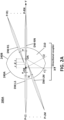
- Figure 2A shows a proposed dielectric structure as bidirectional coupler with power divider/combiner functionality (200A) according to the present invention.
- the proposed structure (200A) comprises a first group of M input access ports in the left in the figure from (P-L1) to (P-LM), which are coupled to the second group of N output access ports on the right in the figure from (P-R1) to (P-RN) via a free propagation region substrate (210).
- the left edge (240A) of the free propagation region, along which the access ports (P-L1) to (P-LM) are laid along, is shaped by the arc of a circle with a radius r1 whose centre OA is closer to the opposite edge (240B) of the free propagation region substrate (210).
- the edge (240B) of the free space propagation region, along which the output access ports (P-R1) to (P-RN) are laid along, is shaped by the arc of a circle with a radius r 2 whose centre OB is closer to the opposite edge (240A) of the free space propagation region.
- the access ports (PL1-PLM), (PR1-PRM) comprise dielectric waveguide structures, in the left in the figure from (DW-L1) to (DW-LM), and in the right in the figure from (DW-R1) to (DW-RN), all comprising tapered ends for this particular example.
- the dielectric waveguide structures couple the electromagnetic energy propagating through them into the free propagation region substrate (210), reducing the insertion losses between ports which are now proportional to the distance between the input and output ports instead of being proportional to the square spacing of the DW structures by a distance d between them which is not constrained by the far-field criterion, wherein: d ⁇ 2 D 2 / ⁇ where D is the largest waveguide structure dimension and ⁇ is the signal wavelength.
- DW structures emit in a specific region that shifts along its axis for varying signal frequency. Since the phase centre is close to the DW tip at high frequencies, any distance between two radiation zones fits the far-field criterion.
- the separation between the access ports (PL1-PLM), (PR1-PRM) is advantageously reduced by the confinement of the electromagnetic energy within the dielectric waveguide, enabling a compact configuration without introducing crosstalk between adjacent access ports.
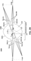
- Figure 2B shows a preferred implementation for another structure (200B).
- the structure (200B) comprises a plurality of arms that allocate the first group of access ports (PL1-PLM) and the second group of access ports (PR1-PRM).
- the structure (200B) includes launching structures for the radio-frequency signal in the dielectric waveguide DW, which advantageously excite only the fundamental mode of the dielectric waveguide DW for every frequency of the operating frequency range.
- the launching structure comprises a tapered end of the dielectric waveguide structure and a tapered slot antenna, both having the same tapering profile.
- the launching structure is shown for all access ports, with tapered slot antennas on the left (TSA-L1 to TSA-LM) and on the right (TSA-R1 to TSA-RN) around the tapered end of the dielectric waveguide structures (DWL1-DWLM), (DWR1-DWRN) having a matching linear tapering profile between the tapered slot antennas and the dielectric waveguide structures.
- the dielectric waveguide structures (DWL1-DWLM), (DWR1-DWRN) have a high-pass filter characteristic, enabling the electrical interconnection of radio-frequency signals with frequencies above a low cut-off frequency ( f CL ).
- the dielectric waveguide structures (DWL1-DWLM), (DWR1-DWRN) can be designed to have a low cut-off frequency ( f CL ) in the microwave range (i.e. between 3 GHz to 30 GHz) or in the millimeter-wave range (i.e. between 30 GHz to 300 GHz), e.g. at an operating frequency of 60 GHz covering a broad frequency range that extends into the Terahertz wave range (i.e. between 300 to 3000 GHz) and beyond.
- the ultra-wideband bidirectional coupler has a low cut-off frequency ( f CL ) of 65 GHz that can be tuned by modifying the structure dimensions.
- the tapered slot antennas (TSA-L1-TSA-LM), (TSA-R1-TSA-RN) have a low-pass filter characteristic, enabling the electrical interconnection of signals from low frequencies up to a high cut-off frequency ( f CH ) in the millimeter-wave range.
- the tapered slot antenna can be designed as a transmission line with contact tips at its extreme with which establish electrical contact with the access port of the device and can be designed to operate over a range that starts at 0 Hz and extends up into the millimeter-wave range (i.e., between 30 GHz to 300 GHz, e.g., at an operating frequency of 100 GHz).
- the tapered slot antennas (TSA-L1-TSA-LM), (TSA-R1-TSA-RN) comprise a tapering profile around a first tapered end of the dielectric waveguide structures (DWL1-DWLM), (DWR1-DWRN).
- DWL1-DWLM dielectric waveguide structures
- DWR1-DWRN dielectric waveguide structures
- the TSA tapering profile and the DW tapering is linear tapered.
- different tapering profiles can be implemented, as e.g. fermi or exponential tapering.
- the tapered slot antennas operate over a frequency range that starts at low frequency and extends above the low cut-off frequency of the dielectric waveguide structure ( f CH > f CL , e.g., above the 60 GHz of previous example).
- the ultra-wideband bidirectional coupler has a higher cut-off frequency ( f CH ) of, at least, 300 GHz.
- the cut-off frequency can be increased e.g. by reducing the thickness of the components of the ultra-wideband bidirectional coupler and/or by using materials with different electrical permittivity.
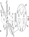
- FIG. 3 shows another bidirectional coupler new bidirectional coupler with power divider/combiner functionality (300) according to the invention.
- the ultra-wideband bidirectional coupler (300) has four access ports, i.e. two input ports (P-L1 and P-L3) and two output ports (P-R4 and P-R2).
- the signal enters to the directional coupler through an input port (P-L1), coupling a defined amount of electromagnetic power to an output transmission port (P-R2) and another amount to a second output, known as coupled port (P-R4).
- P-L3 second input port, known as the isolated port.
- the access ports of the ultra-wideband bidirectional coupler (300) comprise dielectric waveguide structures with tapered ends, dielectric waveguide structure (DW-L1) in the input port (P-L1), dielectric waveguide structure (DW-R2) in the transmission port (P-R2), dielectric waveguide structure (DW-R4) in the coupled port (P-R4) and dielectric waveguide structure (DW-L3) in the isolated port (P-R1).
- the dielectric waveguides structures provide a high-pass filter transfer function operating over a high frequency range starting from a low cut-off frequency ( f CL ) in the microwave range or in the millimeter-wave range.
- the access ports (P-L1), (P-R2), (P-L3) and (P-R4) can include launching structures to inject the signals into their corresponding dielectric waveguides.
- the launching structures comprise a tapered slot antennas and tapered ends of the dielectric waveguide, the tapers of both structures comprise the same tapering profile.
- the tapered slot antennas (TSA-L1), (TSA-R2), (TSA-L3) and (TSA-R4) provide a low-pass characteristic, operating over a low frequency range up to a high cut-off frequency ( f CH ) in the millimeter wave range.
- the tapered slot antennas comprise a matching pattern defining a tapered coupler, preferably a linear tapering profile around the tapered end of the dielectric waveguide at the access port which together with the corresponding tapered end of the dielectric waveguide achieves an ultra-wideband excitation of the directional coupler in a single-mode regime.
- a characteristic of this structure is that allows to control the amount of power coupled from one input port to an output port from the relative angle of their respective locations at the opposite edges of the free propagation region.
- the input port (P-L1) electromagnetic energy is divided between the output ports, (P-R2) and (P-R4).
- the maximum power coupling occurs when the dielectric waveguides of an input port and an output port are located along the same axis, as shown in figure 3 for the Input Port (P-L1) and the Transmission Port (P-R2) of the ultra-wideband bidirectional coupler (300).
- the transmitted signal level between ports (P-L1) and (P-R2) is controlled by the (DW-L1) antenna tapering angle e and the distance between the tips of the (DW-L1, DW-R2) antenna tips, d . Both, smaller e and d lead to larger transmitted signal level.
- the structures (DW-R2) and (DW-R4) may point to the phase centre of the structure (DW-L1).
- the DW structures (DW-L1) and (DW-L3) may point to the phase centre of the DW structure (DW-R2). Since the phase centre of this structure varies with frequency along the antenna axis, a trade-off can be established to select the frequency for which the phase front is pointed, which sets the upper frequency limit to the bandwidth of the structure.
- the DW structure (DW-L1) points toward the DW structure (DW-R2).
- the DW structure (DW-R4) points toward the structure (DW-L1) phase centre at 260 GHz.
- the length c determines the distance between the phase centre and the tip of the DW structure (DW-L1).
- the DW structure (DW-L3) points towards the DW structure (DW-R2) phase centre at 260 GHz.
- the coupling level between an input port and an output port when these are not in the same axis is controlled by the relative angle between their positions, as shown in figure 3 for the input port (P-L1) and the transmission port (P-R4) of the ultra-wideband bidirectional coupler (300).
- the angle a controls the coupling ratio between the input port (P-L1) and the transmission port (P-R4).
- the angle b controls the coupling ratio between the output port (P-R2) and the isolation port (P-L3).
- both angles are equal, but a and b can be designed independently to achieve different coupling ratios between ports (P-L3) and (P-R2) with respect to (P-L1) and (P-R4).
- the coupling ratios are reduced when the angle increases.
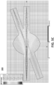
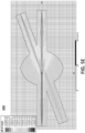
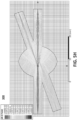
- the tapered slot antenna (TSA-L3) tapering profile (300a) and the DW tapering is linear tapered, as shown in the zoom of figure 3 .
- other tapering profiles can be implemented, as e.g. wherein the tapered slot antenna (TSA-L3) tapering profile (300b) and the DW tapering profile are exponential tapered, or wherein the (TSA-L3) tapering profile (300c) and the DW tapering profile are FERMI tapered.
- absorbers can be placed in the end of the free propagation region (310).
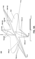
- Figure 4A shows a 3D view of ultra-wideband bidirectional coupler (300) when the dielectric waveguides and the free propagation region, which can be realized with materials of equal or different permittivity, are stacked, i.e. the free propagation region (310), the four DW structures (DW-L1, DW-R2, DW-L3, DW-R4) and the tapered slot antennas (TSA-L1, TSA-R2, TSA-L3, TSA-R4).
- the free propagation region 310
- the four DW structures DW-L1, DW-R2, DW-L3, DW-R4
- TSA-L1, TSA-R2, TSA-L3, TSA-R4 the tapered slot antennas
- an alternative single-layer embodiment is obtained when the DW structures (DW-L1, DW-R2, DW-L3, DW-R4) are embedded within the free propagation region (310) to obtain a more compact system.
- the embedding implies any fabrication method that achieves to create differences in the permittivity within the free propagation region to define a dielectric waveguide structure, i.e. for example, either by etching porosities for reducing the permittivity around the DW structures or by assembling parts of different permittivity.
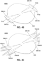
- figure 4B shows a 3D view of ultra-wideband bidirectional coupler (400A), wherein the DW structures (DW-L1, DW-R2, DW-L3, DW-R4) are embedded in the free propagation region (310) and wherein the DW structures (DW-L1, DW-R2, DW-L3, DW-R4) are truncated.
- the DW structures DW-L1, DW-R2, DW-L3, DW-R4
- Figure 4C shows a 3D view of ultra-wideband bidirectional coupler (400B), wherein the DW structures (DW-L1, DW-R2, DW-L3, DW-R4) are embedded in the free propagation region (310) and include the launching structure tapered slot antennas (TSA-L1, TSA-R2, TSA-L3, TSA-R4) at the access ports, wherein the tapered slot antennas are established on the dielectric material of the free propagation region.
- the DW structures DW-L1, DW-R2, DW-L3, DW-R4
- TSA-L1, TSA-R2, TSA-L3, TSA-R4 the launching structure tapered slot antennas
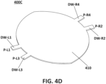
- Figure 4D shows a 3D view of ultra-wideband bidirectional coupler (400C), wherein the free propagation region (310) comprises the same dielectric material as the DW structures and wherein the DW structures have a truncated end.
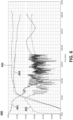
- Figure 6 shows the simulated S parameter amplitude (in dB): S11 (601) (incoming port matching), S21 (602) (transmission between port (P-L1) and (P-R2)), S13 (603) (coupling between the incident port P-L1 and the isolated port P-L3), and S14 (604) (coupling to the coupled port (P-R4)).
- the transmission between ports (P-L1, P-R2), i.e. S21 (602) stays flat from 65 GHz to at least 300 GHz.
- the insertion losses are, approximately 4 dB.
- the coupling (602) between ports (P-L1, P-R4), i.e. S14 (604) is not constant with frequency, leading to a higher coupler directivity at higher frequencies. Due to the smoothness of the curves, this effect can be easily compensated through a path calibration.
- the S11 (601) amplitude port matching is lower than -15 dB for the whole band, and lower than -20 dB for frequencies greater than 80 Ghz.
- the isolation between ports (P-L1, P-L3), i.e. S13 (603) is greater than 25 dB in the whole band.
- the ultra-wideband coupler (300) works as a bidirectional coupler.
- port (P2) works as the source of incident signal
- por (P-L1) works as the transmission port
- port (P-L3) works as the coupled port
- port (P-R4) works as the isolated port.
- port (P-R2) becomes a bi-directional (input and output) port.
- port (P-R2) would be connected to an antenna, a waveguide or a connector.
- an antenna may be placed on port (P-R2).
- port (P-R2) would be connected to the DUT (device under test).
- the signal received in port (P-L3) would be proportional to the DUT incident signal and the signal received in port (P-R4) would be proportional to the signal incident in the DUT.
- Figure 7 shows a coupler (700) that works with a DC extension, which is a solution to extend the operating frequency range of the bidirectional coupler (300) structure in the low frequency range, towards DC.
- the coupler (700) comprises the bidirectional coupler (300) and further comprises a low-frequency directional coupler (750).
- the low-frequency directional coupler (450) comprises ports (P-L1', P-R2', P-L3', P-R4') that are connected to the transmission structures (TSA-L1, TSA-R2, TSA-L3, TSA-R4) ends through metal wires that conforms bifilar lines (720) that can be used for exciting the DW's fundamental mode for all the frequencies above f 0 and suitable for the integration of the low-frequency directional coupler (700).
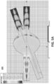
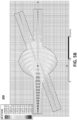
- the signals are efficiently coupled to the DW structures (DW-L1, DW-R2, DW-L3, DW-R4) from the ports through the structures (TSA-L1, TSA-R2, TSA-L3, and TSA-R4), as illustrated in figures 5 and 6 .
- the signal propagates from the ports through a structures TSA though the bifilar lines (720) without being coupled to the DW structures.
- One of several transitions can be incorporated from the bifilar line (720) to the low-frequency directional coupler ports (P-L1', P-R2', P-L3', and P-R4').
- figure 7 shows a low-frequency directional coupler (700) with CPW ports and the transitions between the bifilar lines (720), the CPS and the CPW waveguides.
- the transitions and the low-frequency directional coupler (750) are placed in a substrate (710) that can be placed far enough over (or under) the dielectric coupler (300). Since the waves propagates in the 2D plane (in the free propagation region (210)), there is no radiation in the normal direction a compact configuration can be achieved. The distance between both couplers (300, 750) must be big-enough for avoiding near-field coupling between them.
Landscapes
- Waveguide Aerials (AREA)
- Waveguide Switches, Polarizers, And Phase Shifters (AREA)
- Variable-Direction Aerials And Aerial Arrays (AREA)
Claims (19)
- Bidirektionaler Breitband-Hochfrequenz-Koppler mit Leistungsteiler/Summierer-Funktion (200A, 200B, 300, 400A, 400B, 400C) für Signale mit einer Frequenz von bis zu 300 GHz, umfassend:- ein Substrat (210) mit einem freien Ausbreitungsbereich und einem Paar von gegenüberliegenden Kanten (240A, 240B);- eine entlang einer ersten Kante (240A) des genannten Paars von gegenüberliegenden Kanten (240A, 240B) angeordnete erste Gruppe von Zugangsanschlüssen (P-L1 - P-LM); und- eine entlang einer zweiten Kante (240B) der genannten gegenüberliegenden Kanten (240A, 240B) angeordnete zweite Gruppe von Zugangsanschlüssen (P-R1 - P-RM), wobei die erste und die zweite Gruppe von Zugangsanschlüssen (P-L1 - P-LM), (P-R1 - P-RN) Folgendes umfassen:
dielektrische Wellenleiterstrukturen DW (DW-L1 - DW-LM), (DW-R1 - DW-RN), wobei das Substrat (210) mit freiem Ausbreitungsbereich so ausgebildet ist, dass es als 2D-Ausbreitungsbereich im freien Raum funktioniert, sodass die DW-Strukturen (DW-L1 - DW-LM), (DW-R1 - DW-RN) ausgehend von einer niedrigen Grenzfrequenz fCL im Mikrowellenbereich oder im Millimeterwellenbereich eine Hochpassfilter-Übertragungsfunktion über einen hohen Frequenzbereich bereitstellen. - Bidirektionaler Ultrabreitband-Hochfrequenz-Koppler (200A, 200B, 300, 400A, 400B, 400C) nach Anspruch 1, wobei die erste Kante (240A) des genannten Paars von gegenüberliegenden Kanten als Bogen eines Kreises mit einem Radius r1 geformt ist, dessen Mittelpunkt (OA) näher an der zweiten Kante (240B) liegt.
- Bidirektionaler Ultrabreitband-Hochfrequenz-Koppler (200A, 200B, 300, 400A, 400B, 400C) nach Anspruch 2, wobei die zweite Kante (240B) des genannten Paars von gegenüberliegenden Kanten als Bogen eines zweiten Kreises mit einem Radius r2 geformt ist, dessen Mittelpunkt (OB) näher an der ersten Kante (240B) liegt.
- Bidirektionaler Ultrabreitband-Hochfrequenz-Koppler (200A, 200B, 300, 400A, 400B, 400C) nach Anspruch 3, wobei r1 = r2.
- Bidirektionaler Ultrabreitband-Hochfrequenz-Koppler (200A, 200B, 300, 400A, 400B, 400C) nach den Ansprüchen 1 bis 4, weiter umfassend eine Vielzahl von Armen, wobei die Vielzahl von Armen die erste Gruppe von Zugangsanschlüssen (P-L1 - P-LM) und die zweite Gruppe von Zugangsanschlüssen (P-R1 - P-RN) zuordnet.
- Bidirektionaler Ultrabreitband-Hochfrequenz-Koppler (300) nach den Ansprüchen 1 bis 5, wobei die DW-Strukturen (DW-L1 - DW-LM), (DW-R1 - DW-RN) auf dem Substrat (310) mit freiem Ausbreitungsbereich angeordnet sind.
- Bidirektionaler Ultrabreitband-Hochfrequenz-Koppler (400A, 400B) nach den Ansprüchen 1 bis 5, wobei die DW-Strukturen (DW-L1 - DW-LM), (DW-R1 - DW-RN) in dem Substrat (310) mit freiem Ausbreitungsbereich eingebettet sind.
- Bidirektionaler Ultrabreitband-Hochfrequenz-Koppler (200B, 300) nach einem der vorangehenden Ansprüche, wobei die DW-Strukturen (DW-L1 - DW-LM), (DW-R1 - DW-RN) sich verjüngende Enden mit einem definierten sich verjüngenden Profil umfassen, und wobei die erste und die zweite Gruppe von Zugangsanschlüssen (P-L1 - P-LM), (P-R1 - P-RN) des Weiteren sich verjüngende Schlitzantennen TSA (TSA-L1 - TSA-LM), (TSA-R1 - TSA-RN) umfassen, die eine Bandpassfilter-Übertragungsfunktion über einen niedrigen Frequenzbereich bis zu einer hohen Grenzfrequenz fCH im Millimeterwellenbereich bereitstellen, wobei die TSA (TSA-L1 - TSA-LM), (TSA-R1 - TSA-RN) ein sich verjüngendes TSA-Profil (300a, 300b, 300c) umfassen, wobei das erste sich verjüngende Ende der DW-Strukturen (DW-L1 - DW-LM), (DW-R1 - DW-RN) zwischen den TSA (TSA-L1 - TSA-LM), (TSA-R1 - TSA-RN) liegt, wobei das sich verjüngende TSA-Profil (300a, 300b, 300c) dem sich verjüngenden DW-Profil entspricht.
- Bidirektionaler Ultrabreitband-Hochfrequenz-Koppler (200B) nach Anspruch 8, wobei das sich verjüngende TSA-Profil (300a) und das sich verjüngende DW-Profil linear verjüngt sind.
- Bidirektionaler Ultrabreitband-Hochfrequenz-Koppler (200B) nach Anspruch 8, wobei das sich verjüngende TSA-Profil (300b) und das sich verjüngende DW-Profil exponentiell verjüngt sind.
- Bidirektionaler Ultrabreitband-Hochfrequenz-Koppler (200B) nach Anspruch 8, wobei das sich verjüngende TSA-Profil (300c) und das sich verjüngende DW-Profil FERMI-verjüngt sind.
- Bidirektionaler Ultrabreitband-Koppler (700) nach den Ansprüchen 8 bis 11, welcher des Weiteren Folgendes aufweist:- einen Niederfrequenz-Richtungskoppler (750) mit einem Frequenz-Betriebsbereich, der bei Gleichstrom oder bei einer niedrigen Frequenz im Kilohertzbereich beginnt und bis zu einer niedrigen Grenzfrequenz fDCH im Millimeterwellenbereich reicht,- wobei fDCH > eine niedrige Grenzfrequenz von DW-Strukturen fCL,- eine Vielzahl von Übertragungsleitungen (720) und Wellenleiterübergängen, die den Niederfrequenz-Richtungskoppler (750) und die TSA (TSA-L1 - TSA-LM), (TSA-R1 - TSA-RN) für einen kombinierten Betriebsfrequenzbereich bis zu einer hohen Grenzfrequenz fDCH verbinden.
- Bidirektionaler Ultrabreitband-Koppler (300) nach den Ansprüchen 6 oder 7, umfassend:- zwei erste Zugangsanschlüsse (P-L1 - P-L3) entlang der mindestens einen Kante des genannten Substrats (310) mit freiem Ausbreitungsbereich, welche erste und dritte DW-Strukturen (DW-L1 - DW-L3) mit sich verjüngenden Enden umfassen,- zwei zweite Zugangsanschlüsse (P-R4 - P-R2) entlang der gegenüberliegenden Kante des genannten Substrats (310) mit freiem Ausbreitungsbereich, welche vierte und zweite DW-Strukturen (DW-R4 - DW-R2) mit sich verjüngenden Enden umfassen,- wobei ein sich verjüngendes Ende der ersten DW-Struktur (DW-L1) zu einem sich verjüngenden Ende der zweiten DW-Struktur (DW-R2) zeigt,- wobei ein sich verjüngendes Ende der vierten DW-Struktur (DW-R4) zu einem sich verjüngenden Ende der ersten DW-Struktur (DW-L1) zeigt, und- wobei ein sich verjüngendes Ende der dritten DW-Struktur (DW-L3) zu einem sich verjüngenden Ende der zweiten DW-Struktur (DW-R2) zeigt.
- Bidirektionaler Ultrabreitband-Koppler (300) nach Anspruch 13, wobei die DW-Strukturen (DW-L1 - DW-L3), (DW-R2 - DW-R4) ein sich verjüngendes DW-Profil umfassen, und des Weiteren TSA (TSA-L1 - TSA-L3), (TSA-R2 - TSA-R4) umfasst sind, welche aus einem metallischen Material bestehen, welches eine Verbindung mit Tiefpass-Charakteristik bereitstellt, welche über einen niedrigen Frequenzbereich bis zu einer hohen Grenzfrequenz fCH im Millimeterwellenbereich arbeitet, wobei die TSA (TSA-L1 - TSA-L3), (TSA-R2 - TSA-R4) ein sich verjüngendes TSA-Profil (300a, 300b, 300c) um ein erstes sich verjüngendes Ende der DW-Strukturen (DW-L1 - DW-L3), (DW-R2 - DW-R4) umfassen, wobei das sich verjüngende TSA-Profil (300a, 300b, 300c) dem sich verjüngenden DW-Profil entspricht.
- Bidirektionaler Ultrabreitband-Hochfrequenz-Koppler (400A, 400C) nach den Ansprüchen 1 bis 7, wobei die DW-Strukturen (DW-L1 - DW-LM), (DW-R1 - DW-RN) mindestens ein kegelstumpfförmiges Ende umfassen.
- Bidirektionaler Ultrabreitband-Koppler (200A, 200B, 300, 400A, 400B, 400C) nach einem der vorangehenden Ansprüche, wobei das Substrat (310) mit freiem Ausbreitungsbereich eine andere Permittivität aufweist als die DW-Strukturen (DW-L1 - DW-LM), (DW-R1 - DW-RN).
- Bidirektionaler Ultrabreitband-Koppler (200A, 200B, 300, 400A, 400B, 400C) nach einem der vorangehenden Ansprüche, wobei das Substrat (310) mit freiem Ausbreitungsbereich Absorber umfasst.
- Bidirektionaler Ultrabreitband-Koppler (400C) nach den Ansprüchen 1 bis 3, wobei das Substrat (310) mit freiem Ausbreitungsbereich dielektrisches Material umfasst.
- Bidirektionaler Ultrabreitband-Koppler (200A, 200B, 300, 400A, 400B, 400C) nach den Ansprüchen 2 bis 18, wobei der Bogen des Kreises für die erste Gruppe von Zugangsanschlüssen (P-L1 - P-LM) gleich dem Radius r2 des Bogens des zweiten Kreises ist, und wobei die Mittelpunkte (OA, OB) der beiden Kreise radial ausgerichtet sind.
Priority Applications (6)
| Application Number | Priority Date | Filing Date | Title |
|---|---|---|---|
| EP21382573.0A EP4113737B1 (de) | 2021-06-29 | 2021-06-29 | Bidirektionaler dielektrischer hochfrequenz(hf)-koppler mit leistungsteiler/combiner-funktion |
| ES21382573T ES2999025T3 (en) | 2021-06-29 | 2021-06-29 | Dielectric radio frequency (rf) bidirectional coupler with power divider/combiner functionality |
| PCT/EP2022/067714 WO2023275042A1 (en) | 2021-06-29 | 2022-06-28 | Dielectric radio frequency (rf) bidirectional coupler with power divider/combiner functionality |
| CN202280045662.3A CN117882245A (zh) | 2021-06-29 | 2022-06-28 | 具有功率分配器/合路器功能的介质射频双向耦合器 |
| US18/575,168 US20240313385A1 (en) | 2021-06-29 | 2022-06-28 | Dielectric radio frequency (rf) bidirectional coupler with power divider/combiner functionality |
| JP2023580886A JP7849745B2 (ja) | 2021-06-29 | 2022-06-28 | 電力分割器/合成器機能を有する誘電体無線周波数(rf)双方向性結合器 |
Applications Claiming Priority (1)
| Application Number | Priority Date | Filing Date | Title |
|---|---|---|---|
| EP21382573.0A EP4113737B1 (de) | 2021-06-29 | 2021-06-29 | Bidirektionaler dielektrischer hochfrequenz(hf)-koppler mit leistungsteiler/combiner-funktion |
Publications (3)
| Publication Number | Publication Date |
|---|---|
| EP4113737A1 EP4113737A1 (de) | 2023-01-04 |
| EP4113737C0 EP4113737C0 (de) | 2024-11-13 |
| EP4113737B1 true EP4113737B1 (de) | 2024-11-13 |
Family
ID=76890963
Family Applications (1)
| Application Number | Title | Priority Date | Filing Date |
|---|---|---|---|
| EP21382573.0A Active EP4113737B1 (de) | 2021-06-29 | 2021-06-29 | Bidirektionaler dielektrischer hochfrequenz(hf)-koppler mit leistungsteiler/combiner-funktion |
Country Status (6)
| Country | Link |
|---|---|
| US (1) | US20240313385A1 (de) |
| EP (1) | EP4113737B1 (de) |
| JP (1) | JP7849745B2 (de) |
| CN (1) | CN117882245A (de) |
| ES (1) | ES2999025T3 (de) |
| WO (1) | WO2023275042A1 (de) |
Family Cites Families (4)
| Publication number | Priority date | Publication date | Assignee | Title |
|---|---|---|---|---|
| NL97161C (de) * | 1952-03-01 | |||
| US3558213A (en) * | 1969-04-25 | 1971-01-26 | Bell Telephone Labor Inc | Optical frequency filters using disc cavity |
| JP3045046B2 (ja) * | 1995-07-05 | 2000-05-22 | 株式会社村田製作所 | 非放射性誘電体線路装置 |
| JP3732954B2 (ja) * | 1998-06-29 | 2006-01-11 | 京セラ株式会社 | 方向性結合器 |
-
2021
- 2021-06-29 ES ES21382573T patent/ES2999025T3/es active Active
- 2021-06-29 EP EP21382573.0A patent/EP4113737B1/de active Active
-
2022
- 2022-06-28 WO PCT/EP2022/067714 patent/WO2023275042A1/en not_active Ceased
- 2022-06-28 JP JP2023580886A patent/JP7849745B2/ja active Active
- 2022-06-28 CN CN202280045662.3A patent/CN117882245A/zh active Pending
- 2022-06-28 US US18/575,168 patent/US20240313385A1/en active Pending
Also Published As
| Publication number | Publication date |
|---|---|
| JP2024522925A (ja) | 2024-06-21 |
| EP4113737A1 (de) | 2023-01-04 |
| CN117882245A (zh) | 2024-04-12 |
| JP7849745B2 (ja) | 2026-04-22 |
| US20240313385A1 (en) | 2024-09-19 |
| EP4113737C0 (de) | 2024-11-13 |
| ES2999025T3 (en) | 2025-02-24 |
| WO2023275042A1 (en) | 2023-01-05 |
Similar Documents
| Publication | Publication Date | Title |
|---|---|---|
| US11664589B2 (en) | 5G MIMO antenna array with reduced mutual coupling | |
| CN112259962A (zh) | 基于双模平行波导的双频段共口径天线阵 | |
| US11171396B2 (en) | Broadband polarizing screen with one or more radiofrequency polarizing cells | |
| EP4429018A1 (de) | Hybridkoppler mit dielektrischem substrat und wellenleiterübergang | |
| KR102479577B1 (ko) | 5세대 이동 통신용 주파수 분배 및 결합기와 다중빔 안테나를 포함하는 이중 대역 다중빔 안테나 장치 | |
| WO2018016632A1 (ja) | ダイプレクサ及び送受信システム | |
| Emara et al. | Integrated multiport leaky-wave antenna multiplexer/demultiplexer system for millimeter-wave communication | |
| EP4113737B1 (de) | Bidirektionaler dielektrischer hochfrequenz(hf)-koppler mit leistungsteiler/combiner-funktion | |
| Jaschke et al. | Dual-band stepped-impedance transformer to full-height substrate-integrated waveguide | |
| US20250329910A1 (en) | Directional coupler | |
| CN109473774B (zh) | 新型双极化天线 | |
| EP2025038B1 (de) | Kontinuierlich abstimmbare verzögerungsleitung | |
| Kazemi et al. | Design of a wide band eight-way compact SIW power combiner fed by a low loss GCPW-to-SIW transition | |
| CN118336380A (zh) | 双频双极化无源馈电网络 | |
| US9705175B2 (en) | Waveguide power dividers | |
| CN116190967A (zh) | 一种极化跟踪器及应用 | |
| WO2025039103A1 (en) | Orthomode transducer, transmitter, and receiver | |
| WO2021215161A1 (ja) | 多モード導波管アンテナ | |
| CN112993544B (zh) | 一种x频段多极化多通道微波组件 | |
| Kumar et al. | SIW hydride coupler for mm-wave applications | |
| US12614829B2 (en) | Wide band end launcher for coaxial line to co-planar waveguide | |
| US20250174871A1 (en) | Waveguide coupler with self-contained polarization rotation for integrated waveguides, circuits, and systems | |
| Abbosh et al. | Three-way signal divider with tunable ratio for adaptive transmitting antenna arrays | |
| Dolatsha et al. | Analysis and design of multi-mode dielectric waveguide interconnect with planar excitation | |
| RU2324269C2 (ru) | Конструкция выходного узла передающего канала модуля фазированной антенной решетки |
Legal Events
| Date | Code | Title | Description |
|---|---|---|---|
| PUAI | Public reference made under article 153(3) epc to a published international application that has entered the european phase |
Free format text: ORIGINAL CODE: 0009012 |
|
| STAA | Information on the status of an ep patent application or granted ep patent |
Free format text: STATUS: THE APPLICATION HAS BEEN PUBLISHED |
|
| AK | Designated contracting states |
Kind code of ref document: A1 Designated state(s): AL AT BE BG CH CY CZ DE DK EE ES FI FR GB GR HR HU IE IS IT LI LT LU LV MC MK MT NL NO PL PT RO RS SE SI SK SM TR |
|
| STAA | Information on the status of an ep patent application or granted ep patent |
Free format text: STATUS: REQUEST FOR EXAMINATION WAS MADE |
|
| 17P | Request for examination filed |
Effective date: 20230704 |
|
| RBV | Designated contracting states (corrected) |
Designated state(s): AL AT BE BG CH CY CZ DE DK EE ES FI FR GB GR HR HU IE IS IT LI LT LU LV MC MK MT NL NO PL PT RO RS SE SI SK SM TR |
|
| GRAP | Despatch of communication of intention to grant a patent |
Free format text: ORIGINAL CODE: EPIDOSNIGR1 |
|
| STAA | Information on the status of an ep patent application or granted ep patent |
Free format text: STATUS: GRANT OF PATENT IS INTENDED |
|
| GRAS | Grant fee paid |
Free format text: ORIGINAL CODE: EPIDOSNIGR3 |
|
| GRAA | (expected) grant |
Free format text: ORIGINAL CODE: 0009210 |
|
| STAA | Information on the status of an ep patent application or granted ep patent |
Free format text: STATUS: THE PATENT HAS BEEN GRANTED |
|
| INTG | Intention to grant announced |
Effective date: 20240927 |
|
| AK | Designated contracting states |
Kind code of ref document: B1 Designated state(s): AL AT BE BG CH CY CZ DE DK EE ES FI FR GB GR HR HU IE IS IT LI LT LU LV MC MK MT NL NO PL PT RO RS SE SI SK SM TR |
|
| REG | Reference to a national code |
Ref country code: GB Ref legal event code: FG4D |
|
| REG | Reference to a national code |
Ref country code: CH Ref legal event code: EP |
|
| REG | Reference to a national code |
Ref country code: IE Ref legal event code: FG4D |
|
| REG | Reference to a national code |
Ref country code: DE Ref legal event code: R096 Ref document number: 602021021745 Country of ref document: DE |
|
| U01 | Request for unitary effect filed |
Effective date: 20241202 |
|
| U07 | Unitary effect registered |
Designated state(s): AT BE BG DE DK EE FI FR IT LT LU LV MT NL PT RO SE SI Effective date: 20241211 |
|
| REG | Reference to a national code |
Ref country code: ES Ref legal event code: FG2A Ref document number: 2999025 Country of ref document: ES Kind code of ref document: T3 Effective date: 20250224 |
|
| PG25 | Lapsed in a contracting state [announced via postgrant information from national office to epo] |
Ref country code: HR Free format text: LAPSE BECAUSE OF FAILURE TO SUBMIT A TRANSLATION OF THE DESCRIPTION OR TO PAY THE FEE WITHIN THE PRESCRIBED TIME-LIMIT Effective date: 20241113 Ref country code: IS Free format text: LAPSE BECAUSE OF FAILURE TO SUBMIT A TRANSLATION OF THE DESCRIPTION OR TO PAY THE FEE WITHIN THE PRESCRIBED TIME-LIMIT Effective date: 20250313 |
|
| PG25 | Lapsed in a contracting state [announced via postgrant information from national office to epo] |
Ref country code: NO Free format text: LAPSE BECAUSE OF FAILURE TO SUBMIT A TRANSLATION OF THE DESCRIPTION OR TO PAY THE FEE WITHIN THE PRESCRIBED TIME-LIMIT Effective date: 20250213 |
|
| PG25 | Lapsed in a contracting state [announced via postgrant information from national office to epo] |
Ref country code: GR Free format text: LAPSE BECAUSE OF FAILURE TO SUBMIT A TRANSLATION OF THE DESCRIPTION OR TO PAY THE FEE WITHIN THE PRESCRIBED TIME-LIMIT Effective date: 20250214 |
|
| PG25 | Lapsed in a contracting state [announced via postgrant information from national office to epo] |
Ref country code: PL Free format text: LAPSE BECAUSE OF FAILURE TO SUBMIT A TRANSLATION OF THE DESCRIPTION OR TO PAY THE FEE WITHIN THE PRESCRIBED TIME-LIMIT Effective date: 20241113 |
|
| PG25 | Lapsed in a contracting state [announced via postgrant information from national office to epo] |
Ref country code: RS Free format text: LAPSE BECAUSE OF FAILURE TO SUBMIT A TRANSLATION OF THE DESCRIPTION OR TO PAY THE FEE WITHIN THE PRESCRIBED TIME-LIMIT Effective date: 20250213 |
|
| U20 | Renewal fee for the european patent with unitary effect paid |
Year of fee payment: 5 Effective date: 20250422 |
|
| PG25 | Lapsed in a contracting state [announced via postgrant information from national office to epo] |
Ref country code: SM Free format text: LAPSE BECAUSE OF FAILURE TO SUBMIT A TRANSLATION OF THE DESCRIPTION OR TO PAY THE FEE WITHIN THE PRESCRIBED TIME-LIMIT Effective date: 20241113 |
|
| PG25 | Lapsed in a contracting state [announced via postgrant information from national office to epo] |
Ref country code: SK Free format text: LAPSE BECAUSE OF FAILURE TO SUBMIT A TRANSLATION OF THE DESCRIPTION OR TO PAY THE FEE WITHIN THE PRESCRIBED TIME-LIMIT Effective date: 20241113 |
|
| PG25 | Lapsed in a contracting state [announced via postgrant information from national office to epo] |
Ref country code: CZ Free format text: LAPSE BECAUSE OF FAILURE TO SUBMIT A TRANSLATION OF THE DESCRIPTION OR TO PAY THE FEE WITHIN THE PRESCRIBED TIME-LIMIT Effective date: 20241113 |
|
| PLBE | No opposition filed within time limit |
Free format text: ORIGINAL CODE: 0009261 |
|
| STAA | Information on the status of an ep patent application or granted ep patent |
Free format text: STATUS: NO OPPOSITION FILED WITHIN TIME LIMIT |
|
| PGFP | Annual fee paid to national office [announced via postgrant information from national office to epo] |
Ref country code: ES Payment date: 20250702 Year of fee payment: 5 |
|
| 26N | No opposition filed |
Effective date: 20250814 |
|
| REG | Reference to a national code |
Ref country code: CH Ref legal event code: H13 Free format text: ST27 STATUS EVENT CODE: U-0-0-H10-H13 (AS PROVIDED BY THE NATIONAL OFFICE) Effective date: 20260127 |
|
| PG25 | Lapsed in a contracting state [announced via postgrant information from national office to epo] |
Ref country code: MC Free format text: LAPSE BECAUSE OF FAILURE TO SUBMIT A TRANSLATION OF THE DESCRIPTION OR TO PAY THE FEE WITHIN THE PRESCRIBED TIME-LIMIT Effective date: 20241113 |
|
| GBPC | Gb: european patent ceased through non-payment of renewal fee |
Effective date: 20250629 |
|
| PG25 | Lapsed in a contracting state [announced via postgrant information from national office to epo] |
Ref country code: GB Free format text: LAPSE BECAUSE OF NON-PAYMENT OF DUE FEES Effective date: 20250629 |
|
| PG25 | Lapsed in a contracting state [announced via postgrant information from national office to epo] |
Ref country code: IE Free format text: LAPSE BECAUSE OF NON-PAYMENT OF DUE FEES Effective date: 20250629 |
|
| PG25 | Lapsed in a contracting state [announced via postgrant information from national office to epo] |
Ref country code: CH Free format text: LAPSE BECAUSE OF NON-PAYMENT OF DUE FEES Effective date: 20250630 |