EP4120573A1 - Amplificateur de transimpédance (tia) avec une résistance d'entrée réglable - Google Patents
Amplificateur de transimpédance (tia) avec une résistance d'entrée réglable Download PDFInfo
- Publication number
- EP4120573A1 EP4120573A1 EP22175798.2A EP22175798A EP4120573A1 EP 4120573 A1 EP4120573 A1 EP 4120573A1 EP 22175798 A EP22175798 A EP 22175798A EP 4120573 A1 EP4120573 A1 EP 4120573A1
- Authority
- EP
- European Patent Office
- Prior art keywords
- amplifier
- radio
- coupled
- circuitry
- resistor
- Prior art date
- Legal status (The legal status is an assumption and is not a legal conclusion. Google has not performed a legal analysis and makes no representation as to the accuracy of the status listed.)
- Pending
Links
Images


Classifications
-
- H—ELECTRICITY
- H04—ELECTRIC COMMUNICATION TECHNIQUE
- H04B—TRANSMISSION
- H04B1/00—Details of transmission systems, not covered by a single one of groups H04B3/00 - H04B13/00; Details of transmission systems not characterised by the medium used for transmission
- H04B1/005—Details of transmission systems, not covered by a single one of groups H04B3/00 - H04B13/00; Details of transmission systems not characterised by the medium used for transmission adapting radio receivers, transmitters andtransceivers for operation on two or more bands, i.e. frequency ranges
-
- H—ELECTRICITY
- H04—ELECTRIC COMMUNICATION TECHNIQUE
- H04B—TRANSMISSION
- H04B1/00—Details of transmission systems, not covered by a single one of groups H04B3/00 - H04B13/00; Details of transmission systems not characterised by the medium used for transmission
- H04B1/06—Receivers
- H04B1/16—Circuits
- H04B1/18—Input circuits, e.g. for coupling to an antenna or a transmission line
-
- H—ELECTRICITY
- H03—ELECTRONIC CIRCUITRY
- H03F—AMPLIFIERS
- H03F1/00—Details of amplifiers with only discharge tubes, only semiconductor devices or only unspecified devices as amplifying elements
- H03F1/08—Modifications of amplifiers to reduce detrimental influences of internal impedances of amplifying elements
- H03F1/18—Modifications of amplifiers to reduce detrimental influences of internal impedances of amplifying elements by use of distributed coupling, i.e. distributed amplifiers
-
- H—ELECTRICITY
- H03—ELECTRONIC CIRCUITRY
- H03F—AMPLIFIERS
- H03F1/00—Details of amplifiers with only discharge tubes, only semiconductor devices or only unspecified devices as amplifying elements
- H03F1/56—Modifications of input or output impedances, not otherwise provided for
-
- H—ELECTRICITY
- H03—ELECTRONIC CIRCUITRY
- H03F—AMPLIFIERS
- H03F3/00—Amplifiers with only discharge tubes or only semiconductor devices as amplifying elements
- H03F3/189—High-frequency amplifiers, e.g. radio frequency amplifiers
- H03F3/19—High-frequency amplifiers, e.g. radio frequency amplifiers with semiconductor devices only
- H03F3/193—High-frequency amplifiers, e.g. radio frequency amplifiers with semiconductor devices only with field-effect devices
-
- H—ELECTRICITY
- H03—ELECTRONIC CIRCUITRY
- H03F—AMPLIFIERS
- H03F3/00—Amplifiers with only discharge tubes or only semiconductor devices as amplifying elements
- H03F3/20—Power amplifiers, e.g. Class B amplifiers, Class C amplifiers
- H03F3/24—Power amplifiers, e.g. Class B amplifiers, Class C amplifiers of transmitter output stages
-
- H—ELECTRICITY
- H04—ELECTRIC COMMUNICATION TECHNIQUE
- H04B—TRANSMISSION
- H04B1/00—Details of transmission systems, not covered by a single one of groups H04B3/00 - H04B13/00; Details of transmission systems not characterised by the medium used for transmission
- H04B1/06—Receivers
- H04B1/10—Means associated with receiver for limiting or suppressing noise or interference
-
- H—ELECTRICITY
- H04—ELECTRIC COMMUNICATION TECHNIQUE
- H04B—TRANSMISSION
- H04B1/00—Details of transmission systems, not covered by a single one of groups H04B3/00 - H04B13/00; Details of transmission systems not characterised by the medium used for transmission
- H04B1/06—Receivers
- H04B1/16—Circuits
- H04B1/1638—Special circuits to enhance selectivity of receivers not otherwise provided for
-
- H—ELECTRICITY
- H04—ELECTRIC COMMUNICATION TECHNIQUE
- H04B—TRANSMISSION
- H04B1/00—Details of transmission systems, not covered by a single one of groups H04B3/00 - H04B13/00; Details of transmission systems not characterised by the medium used for transmission
- H04B1/38—Transceivers, i.e. devices in which transmitter and receiver form a structural unit and in which at least one part is used for functions of transmitting and receiving
- H04B1/40—Circuits
-
- H—ELECTRICITY
- H03—ELECTRONIC CIRCUITRY
- H03F—AMPLIFIERS
- H03F2200/00—Indexing scheme relating to amplifiers
- H03F2200/294—Indexing scheme relating to amplifiers the amplifier being a low noise amplifier [LNA]
-
- H—ELECTRICITY
- H03—ELECTRONIC CIRCUITRY
- H03F—AMPLIFIERS
- H03F2200/00—Indexing scheme relating to amplifiers
- H03F2200/451—Indexing scheme relating to amplifiers the amplifier being a radio frequency amplifier
Definitions
- This disclosure relates generally to electronic devices and, more particularly, to electronic devices with wireless communications circuitry.
- An electronic device with wireless communications capabilities has wireless communications circuitry with one or more antennas.
- Wireless receiver circuitry in the wireless communications circuitry uses the antennas to receive radio-frequency signals.
- Signals received by the antennas are fed through a receiver, which often includes a mixer coupled to a transimpedance amplifier. It can be challenging to design a satisfactory receiver for an electronic device.
- An electronic device may include wireless communications circuitry.
- the wireless communications circuitry may include an antenna, a transceiver configured to receive radio-frequency signals from the antenna and to generate corresponding baseband signals, and a baseband processor configured to receive the baseband signals from the transceiver.
- the wireless circuitry can include: an antenna configured to receive a radio-frequency signal; a first amplifier having an input coupled to the antenna and having an output; an oscillator circuit; a mixer having a first input coupled to the output of the first amplifier, having a second input coupled to the oscillator circuit, and having an output with an output impedance; a second amplifier having an input coupled to the output of the mixer; and an adjustable resistor coupled to the input of the second amplifier and configured to compensate for changes in the output impedance of the mixer as the wireless circuitry is operated across the plurality of radio-frequency bands.
- One or more shunt capacitors can be coupled to the input of the second amplifier.
- One or more feedback capacitors and feedback resistors can be coupled across the input and output of the second amplifier.
- the first amplifier can be a low noise amplifier, whereas the second amplifier can be a wideband transimpedance amplifier.
- the adjustable resistor can include multiple resistive strings each having at least one resistor and at least one switch selectively activated and deactivated depending on the operating frequency of the wireless circuitry.
- An aspect of the disclosure provides a method of operating wireless circuitry in a plurality of radio-frequency bands.
- the method can include: using an antenna to receive a radio-frequency signal; using a first amplifier to receive signals from the antenna; using a mixer to receive signals from the first amplifier and to receive signals from an oscillator, the mixer having an output impedance; using a second amplifier to receive signals from the mixer; and tuning an adjustable resistor coupled to an input of the second amplifier to compensate for changes in the output impedance of the mixer as the wireless circuitry is operated across the plurality of radio-frequency bands.
- the adjustable resistor can be tuned to provide a first resistance value when the wireless circuitry is operating in a first radio-frequency band in the plurality of radio-frequency bands and can be tuned to provide a second resistance value greater than the first resistance value when the wireless circuitry is operating in a second radio-frequency band in the plurality of radio-frequency bands greater than the first radio-frequency band.
- An aspect of the disclosure provides an electronic device.
- the electronic device can include: an antenna configured to receive radio-frequency signals; a baseband processor configured to receive baseband signals generated based on the radio-frequency signals; an oscillator; a mixer having a first input coupled to the antenna, having a second input coupled to the oscillator, and having an output; an amplifier having an input coupled to the output of the mixer; and an adjustable resistor coupled to the input of the amplifier.
- the electronic device can also include a control circuit configured to tune the adjustable resistor as a function of the operating frequency of the amplifier.
- One or more shunt capacitors can be coupled to the input of the amplifier.
- One or more feedback capacitors and feedback resistors can be coupled across the input and output of the amplifier.
- the amplifier can be a wideband transimpedance amplifier.
- An electronic device may be provided with wireless receiver circuitry.
- the wireless receiver circuitry may include an antenna, a low noise amplifier configured to receive radio-frequency signals from the antenna, a mixer configured to receive signals from the low noise amplifier and to receive an oscillator signal, and a transimpedance amplifier configured to receive signals from the mixer.
- the wireless receiver circuitry may be operated in multiple radio-frequency bands across multiple standards.
- the mixer can have an output impedance that varies across the different radio-frequency bands.
- An adjustable resistor can be provided at the input of the transimpedance amplifier to compensate for the variation in the mixer output impedance. Configuring and operating the receiver circuitry in this way allows the performance of the transimpedance amplifier to be maintained across the different radio-frequency bands.
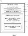
- FIG. 1 is a diagram of an electronic device such as electronic device 10 that can be provided with such wireless receiver circuitry.
- Electronic device 10 may be a computing device such as a laptop computer, a desktop computer, a computer monitor containing an embedded computer, a tablet computer, a cellular telephone, a media player, or other handheld or portable electronic device, a smaller device such as a wristwatch device, a pendant device, a headphone or earpiece device, a device embedded in eyeglasses or other equipment worn on a user's head, or other wearable or miniature device, a television, a computer display that does not contain an embedded computer, a gaming device, a navigation device, an embedded system such as a system in which electronic equipment with a display is mounted in a kiosk or automobile, a wireless internet-connected voice-controlled speaker, a home entertainment device, a remote control device, a gaming controller, a peripheral user input device, a wireless base station or access point, equipment that implements the functionality of two or more of these devices, or other electronic equipment.
- device 10 may include components located on or within an electronic device housing such as housing 12.
- Housing 12 which may sometimes be referred to as a case, may be formed of plastic, glass, ceramics, fiber composites, metal (e.g., stainless steel, aluminum, metal alloys, etc.), other suitable materials, or a combination of these materials.
- parts or all of housing 12 may be formed from dielectric or other low-conductivity material (e.g., glass, ceramic, plastic, sapphire, etc.).
- housing 12 or at least some of the structures that make up housing 12 may be formed from metal elements.
- Control circuitry 14 may include storage such as storage circuitry 16.
- Storage circuitry 16 may include hard disk drive storage, nonvolatile memory (e.g., flash memory or other electrically-programmable-read-only memory configured to form a solid-state drive), volatile memory (e.g., static or dynamic random-access-memory), etc.
- Storage circuitry 16 may include storage that is integrated within device 10 and/or removable storage media.
- Control circuitry 14 may include processing circuitry such as processing circuitry 18. Processing circuitry 18 may be used to control the operation of device 10. Processing circuitry 18 may include on one or more microprocessors, microcontrollers, digital signal processors, host processors, baseband processor integrated circuits, application specific integrated circuits, central processing units (CPUs), etc. Control circuitry 14 may be configured to perform operations in device 10 using hardware (e.g., dedicated hardware or circuitry), firmware, and/or software. Software code for performing operations in device 10 may be stored on storage circuitry 16 (e.g., storage circuitry 16 may include non-transitory (tangible) computer readable storage media that stores the software code). The software code may sometimes be referred to as program instructions, software, data, instructions, or code. Software code stored on storage circuitry 16 may be executed by processing circuitry 18.
- processing circuitry 18 may include on one or more microprocessors, microcontrollers, digital signal processors, host processors, baseband processor integrated circuits, application specific integrated circuits, central processing units (CPUs), etc
- Control circuitry 14 may be used to run software on device 10 such as satellite navigation applications, internet browsing applications, voice-over-internet-protocol (VOIP) telephone call applications, email applications, media playback applications, operating system functions, etc. To support interactions with external equipment, control circuitry 14 may be used in implementing communications protocols.
- VOIP voice-over-internet-protocol
- Communications protocols that may be implemented using control circuitry 14 include internet protocols, wireless local area network (WLAN) protocols (e.g., IEEE 802.11 protocols - sometimes referred to as Wi-Fi ® ), protocols for other short-range wireless communications links such as the Bluetooth ® protocol or other wireless personal area network (WPAN) protocols, IEEE 802.11ad protocols (e.g., ultra-wideband protocols), cellular telephone protocols (e.g., 3G protocols, 4G (LTE) protocols, 5G New Radio (NR) protocols, etc.), MIMO protocols, antenna diversity protocols, satellite navigation system protocols (e.g., global positioning system (GPS) protocols, global navigation satellite system (GLONASS) protocols, etc.), antenna-based spatial ranging protocols (e.g., radio detection and ranging (RADAR) protocols or other desired range detection protocols for signals conveyed at millimeter and centimeter wave frequencies), or any other desired communications protocols.
- Each communications protocol may be associated with a corresponding radio access technology (RAT) that specifies the physical connection methodology used in
- Device 10 may include input-output circuitry 20.
- Input-output circuitry 20 may include input-output devices 22.
- Input-output devices 22 may be used to allow data to be supplied to device 10 and to allow data to be provided from device 10 to external devices.
- Input-output devices 22 may include user interface devices, data port devices, and other input-output components.
- input-output devices 22 may include touch sensors, displays, light-emitting components such as displays without touch sensor capabilities, buttons (mechanical, capacitive, optical, etc.), scrolling wheels, touch pads, key pads, keyboards, microphones, cameras, buttons, speakers, status indicators, audio jacks and other audio port components, digital data port devices, motion sensors (accelerometers, gyroscopes, and/or compasses that detect motion), capacitance sensors, proximity sensors, magnetic sensors, force sensors (e.g., force sensors coupled to a display to detect pressure applied to the display), etc.
- touch sensors displays
- light-emitting components such as displays without touch sensor capabilities, buttons (mechanical, capacitive, optical, etc.), scrolling wheels, touch pads, key pads, keyboards, microphones, cameras, buttons, speakers, status indicators, audio jacks and other audio port components, digital data port devices, motion sensors (accelerometers, gyroscopes, and/or compasses that detect motion), capacitance sensors, proximity sensors, magnetic sensors
- keyboards, headphones, displays, pointing devices such as trackpads, mice, electronic pencil (e.g., a stylus), and joysticks, and other input-output devices may be coupled to device 10 using wired or wireless connections (e.g., some of input-output devices 22 may be peripherals that are coupled to a main processing unit or other portion of device 10 via a wired or wireless link).
- Input-output circuitry 24 may include wireless communications circuitry such as wireless communications circuitry 34 (sometimes referred to herein as wireless circuitry 24) for wirelessly conveying radio-frequency signals. While control circuitry 14 is shown separately from wireless communications circuitry 24 for the sake of clarity, wireless communications circuitry 24 may include processing circuitry that forms a part of processing circuitry 18 and/or storage circuitry that forms a part of storage circuitry 16 of control circuitry 14 (e.g., portions of control circuitry 14 may be implemented on wireless communications circuitry 24). As an example, control circuitry 14 (e.g., processing circuitry 18) may include baseband processor circuitry or other control components that form a part of wireless communications circuitry 24.
- Wireless communications circuitry 24 may include radio-frequency (RF) transceiver circuitry formed from one or more integrated circuits, power amplifier circuitry configured to amplify uplink radio-frequency signals (e.g., radio-frequency signals transmitted by device 10 to an external device), low-noise amplifiers configured to amplify downlink radio-frequency signals (e.g., radio-frequency signals received by device 10 from an external device), passive radio-frequency components, one or more antennas, transmission lines, and other circuitry for handling radio-frequency wireless signals.
- Wireless signals can also be sent using light (e.g., using infrared communications).
- Wireless circuitry 24 may include radio-frequency transceiver circuitry for handling transmission and/or reception of radio-frequency signals in various radio-frequency communications bands.
- the radio-frequency transceiver circuitry may handle wireless local area network (WLAN) communications bands such as the 2.4 GHz and 5 GHz Wi-Fi ® (IEEE 802.11) bands, wireless personal area network (WPAN) communications bands such as the 2.4 GHz Bluetooth ® communications band, cellular telephone communications bands such as a cellular low band (LB) (e.g., 600 to 960 MHz), a cellular low-midband (LMB) (e.g., 1400 to 1550 MHz), a cellular midband (MB) (e.g., from 1700 to 2200 MHz), a cellular high band (HB) (e.g., from 2300 to 2700 MHz), a cellular ultra-high band (UHB) (e.g., from 3300 to 5000 MHz), or other cellular communications bands between about 600 MHz and about 5000 MHz
- radio-frequency transceiver circuitry may sometimes be referred to herein as frequency bands or simply as "bands," and may span corresponding ranges of frequencies.
- the radio-frequency transceiver circuitry within wireless circuitry 24 may cover (handle) any desired frequency bands of interest.
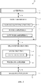
- FIG. 2 is a diagram showing illustrative components within wireless circuitry 24.
- wireless circuitry 24 may include a baseband processor such as baseband processor 26, radio-frequency (RF) transceiver circuitry such as radio-frequency transceiver 28, radio-frequency front end circuitry such as radio-frequency front end module (FEM) 40, and antenna(s) 42.
- Baseband processor 26 may be coupled to transceiver 28 over baseband path 34.
- Transceiver 28 may be coupled to antenna 42 via radio-frequency transmission line path 36.
- Radio-frequency front end module 40 may be interposed on radio-frequency transmission line path 36 between transceiver 28 and antenna 42.
- wireless circuitry 24 is illustrated as including only a single baseband processor 26, a single transceiver 28, a single front end module 40, and a single antenna 42 for the sake of clarity.
- wireless circuitry 24 may include any desired number of baseband processors 26, any desired number of transceivers 36, any desired number of front end modules 40, and any desired number of antennas 42.
- Each baseband processor 26 may be coupled to one or more transceiver 28 over respective baseband paths 34.
- Each transceiver 28 may include one or more transmitters configured to output uplink signals to antenna 42, may include one or more receivers configured to receive downlink signals from antenna 42, and may be coupled to one or more antennas 42 over respective radio-frequency transmission line paths 36.
- Each radio-frequency transmission line path 36 may have a respective front end module 40 interposed thereon. If desired, two or more front end modules 40 may be interposed on the same radio-frequency transmission line path 36. If desired, one or more of the radio-frequency transmission line paths 36 in wireless circuitry 24 may be implemented without any front end module interposed thereon.
- Radio-frequency transmission line path 36 may be coupled to an antenna feed on antenna 42.
- the antenna feed may, for example, include a positive antenna feed terminal and a ground antenna feed terminal.
- Radio-frequency transmission line path 36 may have a positive transmission line signal path such that is coupled to the positive antenna feed terminal on antenna 42.
- Radio-frequency transmission line path 36 may have a ground transmission line signal path that is coupled to the ground antenna feed terminal on antenna 42.
- antennas 42 may be fed using any desired antenna feeding scheme. If desired, antenna 42 may have multiple antenna feeds that are coupled to one or more radio-frequency transmission line paths 36.
- Radio-frequency transmission line path 36 may include transmission lines that are used to route radio-frequency antenna signals within device 10 ( FIG. 1 ).
- Transmission lines in device 10 may include coaxial cables, microstrip transmission lines, stripline transmission lines, edge-coupled microstrip transmission lines, edge-coupled stripline transmission lines, transmission lines formed from combinations of transmission lines of these types, etc.
- Transmission lines in device 10 such as transmission lines in radio-frequency transmission line path 36 may be integrated into rigid and/or flexible printed circuit boards.
- baseband processor 26 may provide baseband signals to transceiver 28 over baseband path 34.
- Transceiver 28 may further include circuitry for converting the baseband signals received from baseband processor 26 into corresponding radio-frequency signals.
- transceiver circuitry 28 may include mixer circuitry 50 for up-converting (or modulating) the baseband signals to radio-frequencies prior to transmission over antenna 42.
- Transceiver circuitry 28 may also include digital-to-analog converter (DAC) and/or analog-to-digital converter (ADC) circuitry for converting signals between digital and analog domains.
- Transceiver 28 may include a transmitter component to transmit the radio-frequency signals over antenna 42 via radio-frequency transmission line path 36 and front end module 40. Antenna 42 may transmit the radio-frequency signals to external wireless equipment by radiating the radio-frequency signals into free space.
- antenna 42 may receive radio-frequency signals from the external wireless equipment.
- the received radio-frequency signals may be conveyed to transceiver 28 via radio-frequency transmission line path 36 and front end module 40.
- Transceiver 28 may include circuitry for converting the received radio-frequency signals into corresponding baseband signals.
- transceiver 28 may use mixer circuitry 50 for down-converting (or demodulating) the received radio-frequency signals to baseband frequencies prior to conveying the received signals to baseband processor 26 over baseband path 34.
- Mixer circuitry 50 can include oscillator circuitry such as a local oscillator 52.
- Local oscillator 52 can generate oscillator signals that mixer circuitry 50 uses to modulate transmitting signals from baseband frequencies to radio frequencies and/or to demodulate the received signals from radio frequencies to baseband or intermediate frequencies.
- Transceiver 28 may further include an amplifier such as amplifier 54 configured to filter signals output from mixer circuitry 50.
- Front end module (FEM) 40 may include radio-frequency front end circuitry that operates on the radio-frequency signals conveyed (transmitted and/or received) over radio-frequency transmission line path 36.
- Front end module may, for example, include front end module (FEM) components such as filter circuitry (e.g., low pass filters, high pass filters, notch filters, band pass filters, radio-frequency coupling/switching circuitry 44 (e.g., radio-frequency coupler, multiplexing circuitry, duplexer circuitry, diplexer circuitry, triplexer circuitry, one or more radio-frequency switches, etc.), radio-frequency amplifier circuitry such as one or more power amplifiers 46 and one or more low noise amplifiers 48, impedance matching circuitry (e.g., circuitry that helps to match the impedance of antenna 42 to the impedance of radio-frequency transmission line 36), antenna tuning circuitry (e.g., networks of capacitors, resistors, inductors, and/or switches that adjust the frequency response of antenna 42), charge pump circuitry,
- Circuitry 44, amplifiers 46 and 48, and other circuitry may be interposed within radio-frequency transmission line path 36, may be incorporated into FEM 40, and/or may be incorporated into antenna 42 (e.g., to support antenna tuning, to support operation in desired frequency bands, etc.). These components, sometimes referred to herein as antenna tuning components, may be adjusted (e.g., using control circuitry 14) to adjust the frequency response and wireless performance of antenna 42 over time.
- Transceiver 28 may be separate from front end module 40.
- transceiver 28 may be formed on another substrate such as the main logic board of device 10, a rigid printed circuit board, or flexible printed circuit that is not a part of front end module 40.
- control circuitry 14 is shown separately from wireless circuitry 24 in the example of FIG. 1 for the sake of clarity, wireless circuitry 24 may include processing circuitry that forms a part of processing circuitry 18 and/or storage circuitry that forms a part of storage circuitry 16 of control circuitry 14 (e.g., portions of control circuitry 14 may be implemented on wireless circuitry 24).
- baseband processor 26 and/or portions of transceiver 28 may form a part of control circuitry 14.
- Control circuitry 14 may provide control signals (e.g., over one or more control paths in device 10) that control the operation of front end module 40.
- Transceiver circuitry 28 may include wireless local area network transceiver circuitry that handles WLAN communications bands (e.g., Wi-Fi ® (IEEE 802.11) or other WLAN communications bands) such as a 2.4 GHz WLAN band (e.g., from 2400 to 2480 MHz), a 5 GHz WLAN band (e.g., from 5180 to 5825 MHz), a Wi-Fi ® 6E band (e.g., from 5925-7125 MHz), and/or other Wi-Fi ® bands (e.g., from 1875-5160 MHz), wireless personal area network transceiver circuitry that handles the 2.4 GHz Bluetooth ® band or other WPAN communications bands, cellular telephone transceiver circuitry that handles cellular telephone bands (e.g., bands from about 600 MHz to about 5 GHz, 3G bands, 4G LTE bands, 5G New Radio Frequency Range 1 (FR1) bands below 10 GHz, 5G New Radio Frequency Range 2 (FR2) bands between 20 and 60 GHz, etc
- Wireless circuitry 24 may include one or more antennas such as antenna 42.
- Antenna 42 may be formed using any desired antenna structures.
- antenna 42 may be an antenna with a resonating element that is formed from loop antenna structures, patch antenna structures, inverted-F antenna structures, slot antenna structures, planar inverted-F antenna structures, helical antenna structures, monopole antennas, dipoles, hybrids of these designs, etc.
- Two or more antennas 42 may be arranged into one or more phased antenna arrays (e.g., for conveying radio-frequency signals at millimeter wave frequencies). Parasitic elements may be included in antenna 42 to adjust antenna performance.
- Antenna 42 may be provided with a conductive cavity that backs the antenna resonating element of antenna 42 (e.g., antenna 42 may be a cavity-backed antenna such as a cavity-backed slot antenna).
- Wireless circuitry 24 may be operable in multiple radio-frequency bands .
- FIG. 3 is a diagram showing wireless circuitry 24 having multiple receiver blocks for handling (receiving) signals from the various radio-frequency bands.
- wireless circuitry 24 may include a first receiver block RX1 configured to receive from antenna 42 signals in a first radio-frequency band group BG1, a second receiver block RX2 configured to receive from antenna 42 signals in a second radio-frequency band group BG2, a third receiver block RX3 configured to receive from antenna 42 signals in a third radio-frequency band group BG3, and so on.
- Each radio-frequency band group may generally include multiple radio-frequency bands. During normal operation, only a selected one of the receiver blocks is activated depending on the desired radio-frequency band of operation.
- BG1 may cover communications in the 0.6 to 1 GHz range
- BG2 may cover communications in the 1 to 1.8 GHz range
- BG3 may cover communications in the 1.8 to 2.3 GHz range.
- These radio-frequency band ranges are merely illustrative. In general, each radio-frequency band can cover 400 MHz, less than 400 MHz, greater than 400 MHz, 500 MHz, 600 MHz, 700 MHz, or other frequency ranges.
- Local oscillator 52 can be used to supply oscillator signals to one or more receiver blocks. For example, a first local oscillator 52 might be used to cover both band groups BG1 and BG2. A second local oscillator 52 might be used to cover only a single band group BG3 (as an example). A third local oscillator 52 might be used to cover three or more band groups.
- wireless circuitry 24 includes three separate receiver blocks for handling different radio-frequency bands is merely illustrative.
- Such type of wireless receiver circuitry is sometimes referred to as a multi-band or multi-standard receiver. If desired, the receiver circuitry may include more or less than three separate receiver blocks.
- Amplifier 54 used within such multi-standard receiver is sometimes referred to herein as a "wideband" amplifier.
- Each of receiver blocks RX1, RX2, and RX3 may include a switching circuit such as radio-frequency switch 44 coupled to antenna 42 (or to a radio-frequency duplexer), a matching circuit such as matching circuit 47, a radio-frequency amplifier such as low noise amplifier (LNA) 48 configured to receive signals from switch 44, and a mixer circuit such as radio-frequency mixer 51 configured to receive amplified signals from low noise amplifier 48 and to receive an oscillator signal from a local oscillator 52.
- Wireless circuitry 24 may include a single amplifier circuit such as amplifier 54 coupled to mixer 51 in each of the multiple receiver blocks.
- Amplifier 54 may, for example, be a transimpedance amplifier (TIA).
- Amplifier 54 may be a wideband amplifier that is capable of handling communications across all of the various radio-frequency band groups (e.g., BG1, BG2, BG3, etc.). Amplifier 54 of this type having a wide bandwidth while being capable of handling communications across multiple radio-frequency bands (standards) is sometimes referred to as a multi-band (multi-standard), wideband amplifier.
- FIG. 4 shows another embodiment in which wireless circuitry 24 is a feedback receiver capable of handling wireless communications in the various radio-frequency bands.
- the feedback receiver of FIG. 4 can be used for power control and calibrating the transmit signal.
- antenna 42 may be coupled to a transmit amplifier such as power amplifier 46 and may be coupled to receiver block RX via a radio-frequency coupler such as directional coupler 44.
- Receiver block RX may further include a radio-frequency attenuating circuit such as attenuator 45 connected to coupler 44, a low noise amplifier (LNA) 48 configured to receive signals from coupler 44 via attenuator 45, and a radio-frequency mixer circuit such as mixer 51 configured to receive signals from low noise amplifier 48 and to receive an oscillator signal from local oscillator 52.
- Mixer 51 may output demodulated signals to amplifier 54.
- Amplifier 54 may be a multi-band, wideband transimpedance amplifier (as an example).
- Receiver block RX may be configured to handle a wide range of radio-frequency bands.
- receiver block RX may be operated in a first mode to handle wireless communications in a first radio-frequency band group from about 0.6 to 1 GHz, in a second mode to handle wireless communications in a second radio-frequency band group from about 1 to 1.8 GHz, in a third mode to handle wireless communications in a third radio-frequency band group from about 1.8 to 2.3 GHz, in a fourth mode to handle wireless communications in a fourth radio-frequency band group from about 2.3 to 2.9 GHz, and so on up to 7 GHz or greater.
- These radio-frequency bands are merely illustrative. The arrangement of FIG.
- the feedback receiver of FIG. 4 in which a single receiver block RX is coupled to transmit amplifier 46 via a directional coupler 44 is sometimes referred to as a feedback receiver architecture.
- the feedback receiver of FIG. 4 generally exhibits a more relaxed noise sensitivity requirement.
- FIG. 5 is a diagram showing additional details at the interface between mixer 51 and transimpedance amplifier 54, which are applicable to the multi-standard receiver of the type described in connection with FIG. 3 , the feedback receiver of the type described in connection with FIG. 4 , and/or other wireless receiver architectures utilizing a wideband amplifier.
- low noise amplifier 48, mixer 51, and transimpedance amplifier 54 may be differential circuits having differential input terminals and differential output terminals.
- a set of shunt capacitors Cmix can be coupled to the output of mixer 51, which is also coupled to the input of amplifier 54.
- a first capacitor Cmix in the set of shunt capacitors has a first terminal coupled to a first input of amplifier 54 and a has a second terminal coupled to a ground power supply line (sometimes referred to as a ground line or ground)
- a second capacitor Cmix in the set of shunt capacitors has a first terminal coupled to a second input of amplifier 54 and has a second terminal coupled to the ground line.
- a set of feedback capacitors Cf can also be coupled across the input and output terminals of amplifier 54.
- a first feedback capacitor Cf in the set of feedback capacitors has a first terminal coupled to the first input of amplifier 54 and has a second terminal coupled to a first output of amplifier 54.
- a second feedback capacitor Cf in the set of feedback capacitors has a first terminal coupled to the second input of amplifier 54 and has a second terminal coupled to a second output of amplifier 54.
- a set of feedback resistors Rf can also be coupled across the input and output terminals of amplifier 54.
- a first feedback resistor Rf in the set of feedback resistors has a first terminal coupled to the first input of amplifier 54 and has a second terminal coupled to the first output of amplifier 54 (i.e., first feedback resistor Rf may be coupled in parallel with first feedback capacitor Cf).
- a second feedback resistor Rf in the set of feedback resistors has a first terminal coupled to the second input of amplifier 54 and has a second terminal coupled to the second output of amplifier 54 (i.e., second feedback resistor Rf may be coupled in parallel with second feedback capacitor Cf).
- transimpedance amplifier 54 and associated components Cmix, Cf, and Rf may be used collectively as a low pass filter circuit to provide low pass filtering functions and may sometimes be referred to as a baseband filter or baseband active filter.
- Each of the capacitors Cmix and/or Cf shown in FIG. 5 may include a bank of switchable capacitors that can be adjusted by controller 64 to optionally tune the bandwidth of the baseband filter.
- Each of the feedback resistors Rf may also include a bank of switchable resistors that can be adjusted by controller 64 to optionally tune the gain of the baseband filter.
- Components Cmix, Cf, and Rf can be adjusted to control the bandwidth of the filter, whereas resistor Rf can be adjusted to control the gain of the filter.
- Mixer 51 may have an output impedance Rout.
- the mixer output impedance Rout may be inversely proportional to the product of Cpar and f LO , where Cpar represents the parasitic capacitance at the output of LNA 48 and where f LO represents the frequency of the oscillator signal generated by local oscillator 52.
- FIG. 6 is a diagram plotting mixer output impedance Rout as a function of oscillator frequency f LO . As shown in FIG. 6 , oscillator frequency f LO may be varied across a wide frequency range (e.g., from 0.6 to 7.2 GHz) when supporting wideband operation.
- Rout Since mixer output impedance Rout is inversely proportional to f LO , Rout decreases as frequency f LO increases (as indicated by curve 60). Curve 60 shows how Rout can vary greatly (e.g., from more than 9 k ⁇ , to less than 3 k ⁇ ) across the wide operating frequency range of the oscillator. These Rout values are merely illustrative. The mixer Rout values can vary widely depending on the intended application and actual design of the receiver.
- the bandwidth and stability of amplifier 54 varies as a function of mixer output impedance Rout.
- large variations in the mixer Rout can potentially degrade the amplifier bandwidth as the receiver operates in the different radio-frequency bands.
- One way of maintaining the target bandwidth of amplifier 54 as the mixer Rout varies is to tune the shunt capacitor(s) Cmix. Tuning Cmix and/or Cf to compensate for changes in mixer Rout can, however, cause the quality factor and the phase margin of amplifier 54 to change, which makes it challenging to design a receiver that satisfies performance criteria across all operating frequencies.
- an adjustable resistive circuit such as adjustable resistor Rin is coupled to the input of amplifier 54 to adjust the input impedance of amplifier 54 to help compensate for variations in mixer output impedance Rout (see, e.g., FIG. 5 ).
- Adjustable resistor Rin may have a first terminal coupled to the first input of amplifier 54 and a second terminal coupled to the second input of amplifier 54 (e.g., resistor Rin may be coupled across the differential input terminals of amplifier 54). Connected in this way, adjustable resistor Rin is effectively coupled in parallel with the mixer output impedance Rout.
- FIG. 7 is a diagram plotting the resistance of adjustable resistor Rin as a function of oscillator frequency f LO .
- resistor Rin may be tuned to exhibit an increasing resistance (i.e., an increasing real impedance value) as oscillator frequency f LO is increased.
- Resistor Rin should be tuned such that the total parallel resistance of Rout and Rin remains constant across all of the radio-frequency bands of interest. Operated in this way, adjustable resistor Rin can be used to maintain the bandwidth of amplifier 54 by compensating for changes in the mixer Rout across the entire range of operating frequencies (e.g., Rin is increased when the mixer Rout decreases, and vice versa).
- adjustable (tunable) resistor Rin to compensate for variations in mixer Rout obviates the need to tune shunt capacitor(s) Cmix when changing from one operating frequency band to another, which can help ensure that the Q factor and the phase margin of amplifier 54 meets performance criteria across the entire range of operating frequencies.
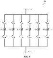
- FIG. 8 shows one suitable implementation of adjustable resistor Rin.
- resistor Rin can have multiple strings of resistors coupled together in parallel between terminals 70 and 72.
- Terminal 70 may be coupled to the first input terminal of amplifier 54, whereas terminal 72 may be coupled to the second input terminal of amplifier 54.
- Adjustable resistor Rin may include multiple resistive strings such as a first resistor string having resistors R1a and R1b selectively activated by switch S1 (e.g., switch S1 may be coupled in series between resistors R1a and R1b), a second resistor string having resistors R2a and R2b selectively activated by switch S2 (e.g., switch S2 may be coupled in series between resistors R2a and R2b), a third resistor string having resistors R3a and R3b selectively activated by switch S3 (e.g., switch S3 may be coupled in series between resistors R3a and R3b), and so on.
- Switches S1-S6 can be controlled by a switch control circuit such as control circuit 64 of FIG. 5 .
- Switch control circuit 64 may be part of control circuitry 14 (see, e.g., FIG. 1 ).
- resistor Rin can have any desired number of resistor strings.
- the various resistor strings in Rin can have the same resistance value or different resistance values.
- the on resistance of each resistor string in adjustable resistor Rin can be selected to provide the desired range of resistance to compensate for changes in the mixer Rout (e.g., such that different switch configurations can provide the corresponding compensation value of Rin as shown in curve 62 of FIG. 7 depending on the operating frequency of the wireless receiver). For example, when operating in the highest radio-frequency band, all of the Rin switches can be turned off (deactivated).
- Control circuit 64 may store a lookup table (as an example) that determines which group of switches to activate depending on the current operating frequency. The gain, bandwidth, linearity, noise, and phase margin of amplifier 54 can be maintained for all resistance values of Rin.
- adjustable resistor Rin (sometimes referred to as a resistor circuit or a resistive circuit having real impedance values) may include: a first resistor string having resistor R1 selectively activated by switches S1a and S1b (e.g., resistor R1 may be coupled in series between switches S1a and S1b); a second resistor string having resistor R2 selectively activated by switches S2a and S2b (e.g., resistor R2 may be coupled in series between switches S2a and S2b); a third resistor string having resistor R3 selectively activated by switches S3a and S2b (e.g., resistor R3 may be coupled in series between switches S3a and S3b), and so on. These switches can be controlled by a first resistor string having resistor R1 selectively activated by switches S1a and S1b (e.g., resistor R1 may be coupled in series between switches S1a and S1b); a second resistor string having resistor R2 selectively activated by switches
- resistor Rin can have any desired number of resistor strings.
- the various resistor strings in Rin can have the same resistance value or different resistance values.
- the on resistance of each resistor string in adjustable resistor Rin can be selected to provide the desired range of resistance to compensate for changes in the mixer Rout (e.g., such that different switch configurations can provide the corresponding compensation value of Rin as shown in curve 62 of FIG. 7 depending on the operating frequency of the wireless receiver).
- the gain, bandwidth, linearity, noise, and phase margin of amplifier 54 can be maintained for all resistance values of Rin.
- each resistor string might only have one resistor and one switch (e.g., the first resistor string can have only resistor R1 coupled in series with S1a while omitting S1b; the second resistor string can have only resistor T2 coupled in series with S2a while omitting S2b; etc.)
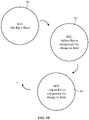
- FIG. 10 is a diagram showing different modes of operation for receiver circuitry of the type shown in connection with FIGS. 1-9 .
- the receiver circuitry can be operated in a first mode such as mode 80 during which the receiver receives signals in a first radio-frequency band group BG1, in a second mode such as mode 82 during which the receiver receives signals in a second radio-frequency band group BG2, in a third mode such as mode 84 during which the receiver receives signals in a third radio-frequency band group BG3, and so on.
- adjustable resistor Rin may be set to its minimum value Rlow by activating all or almost all of its resistor strings.
- adjustable resistor Rin may be adjusted to a different value to compensate for changes in the mixer Rout that result from switching from another mode to mode 82.
- mode 84 when operating in BG3 (e.g., the next operating band group above BG2), adjustable resistor Rin may be adjusted to a different value to compensate for changes in the mixer Rout that result from switching from another mode to mode 84.
- the receiver circuitry can be operated in n different modes of operation, where n can be equal to 5 or more, 6-10, 11-15, more than 10, or other suitable values.
- the methods and operations described above in connection with FIGS. 1-10 may be performed by the components of device 10 using software, firmware, and/or hardware (e.g., dedicated circuitry or hardware).
- Software code for performing these operations may be stored on non-transitory computer readable storage media (e.g., tangible computer readable storage media) stored on one or more of the components of device 10 (e.g., storage circuitry 16 and/or wireless communications circuitry 24 of FIG. 1 ).
- the software code may sometimes be referred to as software, data, instructions, program instructions, or code.
- the non-transitory computer readable storage media may include drives, non-volatile memory such as non-volatile random-access memory (NVRAM), removable flash drives or other removable media, other types of random-access memory, etc.
- NVRAM non-volatile random-access memory
- Software stored on the non-transitory computer readable storage media may be executed by processing circuitry on one or more of the components of device 10 (e.g., processing circuitry in wireless circuitry 24, processing circuitry 18 of FIG. 1 , etc.).
- the processing circuitry may include microprocessors, application processors, digital signal processors, central processing units (CPUs), application-specific integrated circuits with processing circuitry, or other processing circuitry.
- wireless circuitry operable in a plurality of radio-frequency bands includes a first amplifier configured to receive a radio-frequency signal via an antenna, a mixer having a first input coupled to an output of the first amplifier, a second input coupled to an oscillator circuit, and an output, a second amplifier having an input coupled to the output of the mixer and an adjustable resistance coupled to the input of the second amplifier and configured to adjust an input impedance of the second amplifier as the wireless circuitry is operated across the plurality of radio-frequency bands.
- the wireless circuitry includes a control circuit configured to increase a resistance value of the adjustable resistance as an output impedance of the mixer is decreased and to decrease the resistance value of the adjustable resistance as the output impedance of the mixer is increased.
- the input of the second amplifier includes a first amplifier input terminal and a second amplifier input terminal and the adjustable resistance has a first terminal coupled to the first amplifier input terminal and a second terminal coupled to the second amplifier input terminal.
- the wireless circuitry includes a first shunt capacitor having a first terminal coupled to the first amplifier input terminal and having a second terminal coupled to a ground line and a second shunt capacitor having a first terminal coupled to the second amplifier input terminal and having a second terminal coupled to the ground line.
- the wireless circuitry includes a first feedback capacitor having a first terminal coupled to the first amplifier input terminal and having a second terminal coupled to a first amplifier output terminal of the second amplifier and a second feedback capacitor having a first terminal coupled to the second amplifier input terminal and having a second terminal coupled to a second amplifier output terminal of the second amplifier.
- the wireless circuitry includes a first feedback resistor having a first terminal coupled to the first amplifier input terminal and having a second terminal coupled to the first amplifier output terminal and a second feedback resistor having a first terminal coupled to the second amplifier input terminal and having a second terminal coupled to the second amplifier output terminal.
- the second amplifier includes a transimpedance amplifier.
- the adjustable resistance includes a plurality of resistive strings and each resistive string in the plurality of resistive strings includes a first resistor, a second resistor, and a switch coupled between the first and second resistors in that resistive string.
- the adjustable resistance includes a plurality of resistive strings and each resistive string in the plurality of resistive strings includes a first switch, a second switch, and a resistor coupled between the first and second switches in that resistive string.
- a method of operating wireless circuitry in a plurality of radio-frequency bands includes receiving signals at a first amplifier via an antenna, mixing signals from the first amplifier and signals from an oscillator at a mixer having an output impedance, receiving signals at a second amplifier from the mixer and tuning an adjustable resistor coupled to an input of the second amplifier based on changes in the output impedance of the mixer as the wireless circuitry is operated across the plurality of radio-frequency bands.
- the adjustable resistor includes a plurality of resistive strings each having a first resistor, a second resistor, and a switch coupled between the first and second resistors in that resistive string and tuning the adjustable resistor includes selectively activating and deactivating the switch in each of the plurality of resistive strings.
- the adjustable resistor includes a plurality of resistive strings each having a first switch, a second switch, and a resistor coupled between the first and second switches in that resistive string and tuning the adjustable resistor includes selectively activating and deactivating the first and second switches in each of the plurality of resistive strings.
- tuning the adjustable resistor includes tuning the adjustable resistor to provide a first resistance value when the wireless circuitry is operating in a first radio-frequency band in the plurality of radio-frequency bands and tuning the adjustable resistor to provide a second resistance value different than the first resistance value when the wireless circuitry is operating in a second radio-frequency band in the plurality of radio-frequency bands.
- tuning the adjustable resistor includes tuning the adjustable resistor to provide a first resistance value when the wireless circuitry is operating in a first radio-frequency band in the plurality of radio-frequency bands and tuning the adjustable resistor to provide a second resistance value greater than the first resistance value when the wireless circuitry is operating in a second radio-frequency band in the plurality of radio-frequency bands greater than the first radio-frequency band.
- the second amplifier includes a transimpedance amplifier having a bandwidth that is greater than 100 MHz.
- an electronic device includes a mixer having a first input coupled to an antenna, a second input coupled to an oscillator, and an output, an amplifier having an input coupled to the output of the mixer, an adjustable resistance coupled to the input of the amplifier and processing circuitry configured to receive data generated based on signals output by the amplifier.
- the electronic device includes a control circuit configured to tune the adjustable resistance as a function of the operating frequency of the amplifier.
- the input of the amplifier includes a first amplifier input terminal and a second amplifier input terminal and the adjustable resistance has a first resistor terminal coupled to the first amplifier input terminal and a second resistor terminal coupled to the second amplifier input terminal.
- the electronic device includes a first shunt capacitor having a first terminal coupled to the first amplifier input terminal and having a second terminal coupled to a ground line and a second shunt capacitor having a first terminal coupled to the second amplifier input terminal and having a second terminal coupled to the ground line.
- the amplifier includes a first amplifier output terminal and a second amplifier output terminal and the electronic device includes a first feedback capacitor having a first terminal coupled to the first amplifier input terminal and having a second terminal coupled to the first amplifier output terminal, a second feedback capacitor having a first terminal coupled to the second amplifier input terminal and having a second terminal coupled to the second amplifier output terminal, a first feedback resistor having a first terminal coupled to the first amplifier input terminal and having a second terminal coupled to the first amplifier output terminal and a second feedback resistor having a first terminal coupled to the second amplifier input terminal and having a second terminal coupled to the second amplifier output terminal.
Landscapes
- Engineering & Computer Science (AREA)
- Computer Networks & Wireless Communication (AREA)
- Signal Processing (AREA)
- Power Engineering (AREA)
- Input Circuits Of Receivers And Coupling Of Receivers And Audio Equipment (AREA)
- Transceivers (AREA)
- Amplifiers (AREA)
- Microelectronics & Electronic Packaging (AREA)
Priority Applications (1)
| Application Number | Priority Date | Filing Date | Title |
|---|---|---|---|
| EP22197002.3A EP4131787B1 (fr) | 2021-07-14 | 2022-05-27 | Amplificateur d'adaptation d'impédance (tia) à résistance d'entrée accordable |
Applications Claiming Priority (1)
| Application Number | Priority Date | Filing Date | Title |
|---|---|---|---|
| US17/375,843 US11595069B2 (en) | 2021-07-14 | 2021-07-14 | Transimpedance amplifier (TIA) with tunable input resistance |
Related Child Applications (2)
| Application Number | Title | Priority Date | Filing Date |
|---|---|---|---|
| EP22197002.3A Division EP4131787B1 (fr) | 2021-07-14 | 2022-05-27 | Amplificateur d'adaptation d'impédance (tia) à résistance d'entrée accordable |
| EP22197002.3A Division-Into EP4131787B1 (fr) | 2021-07-14 | 2022-05-27 | Amplificateur d'adaptation d'impédance (tia) à résistance d'entrée accordable |
Publications (1)
| Publication Number | Publication Date |
|---|---|
| EP4120573A1 true EP4120573A1 (fr) | 2023-01-18 |
Family
ID=82117360
Family Applications (2)
| Application Number | Title | Priority Date | Filing Date |
|---|---|---|---|
| EP22175798.2A Pending EP4120573A1 (fr) | 2021-07-14 | 2022-05-27 | Amplificateur de transimpédance (tia) avec une résistance d'entrée réglable |
| EP22197002.3A Active EP4131787B1 (fr) | 2021-07-14 | 2022-05-27 | Amplificateur d'adaptation d'impédance (tia) à résistance d'entrée accordable |
Family Applications After (1)
| Application Number | Title | Priority Date | Filing Date |
|---|---|---|---|
| EP22197002.3A Active EP4131787B1 (fr) | 2021-07-14 | 2022-05-27 | Amplificateur d'adaptation d'impédance (tia) à résistance d'entrée accordable |
Country Status (7)
| Country | Link |
|---|---|
| US (2) | US11595069B2 (fr) |
| EP (2) | EP4120573A1 (fr) |
| JP (1) | JP7382452B2 (fr) |
| KR (2) | KR102765809B1 (fr) |
| CN (1) | CN115700996B (fr) |
| AU (1) | AU2022205214B2 (fr) |
| BR (1) | BR102022010813A2 (fr) |
Families Citing this family (3)
| Publication number | Priority date | Publication date | Assignee | Title |
|---|---|---|---|---|
| US11595069B2 (en) * | 2021-07-14 | 2023-02-28 | Apple Inc. | Transimpedance amplifier (TIA) with tunable input resistance |
| KR20240031787A (ko) * | 2022-09-01 | 2024-03-08 | 삼성전자주식회사 | 전류-전압 변환기, 송수신기 및 무선 통신 장치 |
| US20250112658A1 (en) * | 2023-09-29 | 2025-04-03 | Silicon Laboratories Inc. | Wide-band peak detection for an rf receiver |
Citations (5)
| Publication number | Priority date | Publication date | Assignee | Title |
|---|---|---|---|---|
| US8406358B1 (en) * | 2008-02-14 | 2013-03-26 | Marvell International Ltd. | Radio-frequency apparatus with programmable performance and associated methods |
| US20150084688A1 (en) * | 2013-09-25 | 2015-03-26 | Qualcomm Incorporated | Baseband processing circuitry |
| WO2016076981A1 (fr) * | 2014-11-14 | 2016-05-19 | Qualcomm Incorporated | Architecture sans onde acoustique de surface pour des récepteurs |
| US10153934B1 (en) * | 2017-10-11 | 2018-12-11 | Qualcomm Incorporated | Reconfigurable wideband current-mode filters |
| US20210105007A1 (en) * | 2019-10-07 | 2021-04-08 | Samsung Electronics Co., Ltd. | Reconfigurable analog filter and integrated circuit including the same |
Family Cites Families (22)
| Publication number | Priority date | Publication date | Assignee | Title |
|---|---|---|---|---|
| US3409848A (en) | 1967-10-30 | 1968-11-05 | Bell Telephone Labor Inc | Elastic surface waveguide |
| JPS5841506B2 (ja) * | 1980-04-09 | 1983-09-12 | 株式会社リコー | 静電潜像用現像剤 |
| US5442321A (en) | 1993-07-08 | 1995-08-15 | Anadigics, Inc. | Automatic transimpedance control amplifier |
| FI107657B (fi) | 1998-03-11 | 2001-09-14 | Nokia Mobile Phones Ltd | Kytkentä differentiaalisen aktiivikomponentin impedanssin säätämiseksi |
| US6313705B1 (en) * | 1999-12-20 | 2001-11-06 | Rf Micro Devices, Inc. | Bias network for high efficiency RF linear power amplifier |
| US6404281B1 (en) | 2000-11-14 | 2002-06-11 | Sirenza Microdevices, Inc. | Wide dynamic range transimpedance amplifier |
| US8577305B1 (en) * | 2007-09-21 | 2013-11-05 | Marvell International Ltd. | Circuits and methods for generating oscillating signals |
| EP2210338B1 (fr) * | 2007-11-05 | 2012-08-01 | Nxp B.V. | Architecture de mélangeur |
| JP2009253728A (ja) * | 2008-04-08 | 2009-10-29 | Panasonic Corp | 高周波電力増幅器 |
| JP2010147988A (ja) | 2008-12-22 | 2010-07-01 | Toshiba Corp | 増幅回路および無線受信機 |
| US8089309B2 (en) | 2009-06-26 | 2012-01-03 | Bae Systems Information And Electronic Systems Integration Inc. | Transimpedance amplifier input stage mixer |
| US8594603B2 (en) | 2009-11-08 | 2013-11-26 | The Trustees Of Columbia University In The City Of New York | Systems and methods for cancelling interferers in a receiver |
| CN101867346B (zh) * | 2010-05-31 | 2013-07-03 | 广州市广晟微电子有限公司 | 基于无源混频器的信号混频方法和零中频接收机 |
| US8452253B2 (en) | 2010-07-20 | 2013-05-28 | Broadcom Corporation | Compact low-power receiver including transimpedance amplifier, digitally controlled interface circuit, and low pass filter |
| US8831551B2 (en) * | 2012-01-20 | 2014-09-09 | Mediatek Inc. | Receiver |
| US20130214979A1 (en) * | 2012-02-17 | 2013-08-22 | Emily B. McMilin | Electronic Device Antennas with Filter and Tuning Circuitry |
| JP5841506B2 (ja) * | 2012-08-08 | 2016-01-13 | ルネサスエレクトロニクス株式会社 | 半導体集積回路及びそれを備えた無線通信端末 |
| US8841972B2 (en) * | 2012-10-19 | 2014-09-23 | Texas Instruments Deutschland Gmbh | Electronic device, fiber-optic communication system comprising the electronic device and method of operating the electronic device |
| US9356636B1 (en) * | 2015-02-06 | 2016-05-31 | University Of Macau | RF-to-BB-current-reuse wideband receiver with parallel N-path active/passive mixers |
| US9800280B2 (en) | 2016-01-12 | 2017-10-24 | Qualcomm Incorporated | Noise suppression in radio frequency receivers |
| CN110661538B (zh) * | 2019-09-11 | 2021-05-14 | 芯原微电子(上海)股份有限公司 | 低功耗全自动调整宽带接收机射频前端 |
| US11595069B2 (en) * | 2021-07-14 | 2023-02-28 | Apple Inc. | Transimpedance amplifier (TIA) with tunable input resistance |
-
2021
- 2021-07-14 US US17/375,843 patent/US11595069B2/en active Active
-
2022
- 2022-05-27 EP EP22175798.2A patent/EP4120573A1/fr active Pending
- 2022-05-27 EP EP22197002.3A patent/EP4131787B1/fr active Active
- 2022-06-02 BR BR102022010813-7A patent/BR102022010813A2/pt unknown
- 2022-06-07 KR KR1020220068866A patent/KR102765809B1/ko active Active
- 2022-06-07 CN CN202210637930.2A patent/CN115700996B/zh active Active
- 2022-06-10 JP JP2022094158A patent/JP7382452B2/ja active Active
- 2022-07-13 AU AU2022205214A patent/AU2022205214B2/en active Active
- 2022-09-15 US US17/945,226 patent/US11791856B2/en active Active
-
2024
- 2024-07-30 KR KR1020240101176A patent/KR102731658B1/ko active Active
Patent Citations (5)
| Publication number | Priority date | Publication date | Assignee | Title |
|---|---|---|---|---|
| US8406358B1 (en) * | 2008-02-14 | 2013-03-26 | Marvell International Ltd. | Radio-frequency apparatus with programmable performance and associated methods |
| US20150084688A1 (en) * | 2013-09-25 | 2015-03-26 | Qualcomm Incorporated | Baseband processing circuitry |
| WO2016076981A1 (fr) * | 2014-11-14 | 2016-05-19 | Qualcomm Incorporated | Architecture sans onde acoustique de surface pour des récepteurs |
| US10153934B1 (en) * | 2017-10-11 | 2018-12-11 | Qualcomm Incorporated | Reconfigurable wideband current-mode filters |
| US20210105007A1 (en) * | 2019-10-07 | 2021-04-08 | Samsung Electronics Co., Ltd. | Reconfigurable analog filter and integrated circuit including the same |
Non-Patent Citations (1)
| Title |
|---|
| ATALLA ESSAM S ET AL: "Novel analysis of passive mixer output impedance using switched-capacitor techniques", 2013 IEEE 56TH INTERNATIONAL MIDWEST SYMPOSIUM ON CIRCUITS AND SYSTEMS (MWSCAS), IEEE, 4 August 2013 (2013-08-04), pages 625 - 628, XP032525525, ISSN: 1548-3746, ISBN: 978-1-4799-4134-6, [retrieved on 20131124], DOI: 10.1109/MWSCAS.2013.6674726 * |
Also Published As
| Publication number | Publication date |
|---|---|
| EP4131787A1 (fr) | 2023-02-08 |
| KR20230011864A (ko) | 2023-01-25 |
| EP4131787B1 (fr) | 2026-02-25 |
| JP7382452B2 (ja) | 2023-11-16 |
| US20230019152A1 (en) | 2023-01-19 |
| KR102731658B1 (ko) | 2024-11-18 |
| JP2023013964A (ja) | 2023-01-26 |
| CN115700996B (zh) | 2023-08-01 |
| BR102022010813A2 (pt) | 2023-01-24 |
| KR20240121199A (ko) | 2024-08-08 |
| AU2022205214A1 (en) | 2023-02-02 |
| CN115700996A (zh) | 2023-02-07 |
| AU2022205214B2 (en) | 2024-01-11 |
| US11791856B2 (en) | 2023-10-17 |
| KR102765809B1 (ko) | 2025-02-11 |
| US20230015681A1 (en) | 2023-01-19 |
| US11595069B2 (en) | 2023-02-28 |
Similar Documents
| Publication | Publication Date | Title |
|---|---|---|
| KR102731658B1 (ko) | 동조가능한 입력 저항을 갖는 트랜스임피던스 증폭기(tia) | |
| US11664844B2 (en) | Amplifier circuitry for carrier aggregation | |
| US11843356B2 (en) | Radio-frequency power amplifier with amplitude modulation to amplitude modulation (AMAM) compensation | |
| US20250105802A1 (en) | Gain Reduction Techniques for Radio-frequency Amplifiers | |
| EP4148994A1 (fr) | Circuit d'amplificateur avec réglages de gain et adaptation d'entrée | |
| EP4148990B1 (fr) | Amplificateur de puissance radiofréquence avec compensation de la modulation d'amplitude à la modulation de phase (am-pm) | |
| EP4148991A1 (fr) | Amplificateur de puissance radiofréquence avec compensation de la modulation d'amplitude à la modulation de phase (am-pm) | |
| US20250096743A1 (en) | Wireless Circuitry with Tunable Matching Network | |
| CN115700997A (zh) | 具有可调谐输入电阻的跨阻放大器(tia) | |
| EP4718733A1 (fr) | Déphaseur actif à coupleur hybride en quadrature | |
| US20260088767A1 (en) | Current-Sharing Amplifier Circuitry | |
| US20240364366A1 (en) | Wireless Circuitry having Power Control Loop with Interference Suppression Filter | |
| US20260081575A1 (en) | Notch Filter for Wireless Circuitry | |
| KR20260025007A (ko) | 능동 튜닝가능 다중대역 필터 회로부 |
Legal Events
| Date | Code | Title | Description |
|---|---|---|---|
| PUAI | Public reference made under article 153(3) epc to a published international application that has entered the european phase |
Free format text: ORIGINAL CODE: 0009012 |
|
| STAA | Information on the status of an ep patent application or granted ep patent |
Free format text: STATUS: REQUEST FOR EXAMINATION WAS MADE |
|
| 17P | Request for examination filed |
Effective date: 20220527 |
|
| AK | Designated contracting states |
Kind code of ref document: A1 Designated state(s): AL AT BE BG CH CY CZ DE DK EE ES FI FR GB GR HR HU IE IS IT LI LT LU LV MC MK MT NL NO PL PT RO RS SE SI SK SM TR |
|
| STAA | Information on the status of an ep patent application or granted ep patent |
Free format text: STATUS: EXAMINATION IS IN PROGRESS |
|
| 17Q | First examination report despatched |
Effective date: 20250211 |