EP4123271A1 - Dispositif photographique - Google Patents
Dispositif photographique Download PDFInfo
- Publication number
- EP4123271A1 EP4123271A1 EP20925147.9A EP20925147A EP4123271A1 EP 4123271 A1 EP4123271 A1 EP 4123271A1 EP 20925147 A EP20925147 A EP 20925147A EP 4123271 A1 EP4123271 A1 EP 4123271A1
- Authority
- EP
- European Patent Office
- Prior art keywords
- sub
- light source
- image
- imaging device
- reflector
- Prior art date
- Legal status (The legal status is an assumption and is not a legal conclusion. Google has not performed a legal analysis and makes no representation as to the accuracy of the status listed.)
- Withdrawn
Links
Images





Classifications
-
- G—PHYSICS
- G02—OPTICS
- G02B—OPTICAL ELEMENTS, SYSTEMS OR APPARATUS
- G02B5/00—Optical elements other than lenses
- G02B5/02—Diffusing elements; Afocal elements
- G02B5/0273—Diffusing elements; Afocal elements characterized by the use
- G02B5/0284—Diffusing elements; Afocal elements characterized by the use used in reflection
-
- G—PHYSICS
- G01—MEASURING; TESTING
- G01N—INVESTIGATING OR ANALYSING MATERIALS BY DETERMINING THEIR CHEMICAL OR PHYSICAL PROPERTIES
- G01N21/00—Investigating or analysing materials by the use of optical means, i.e. using sub-millimetre waves, infrared, visible or ultraviolet light
- G01N21/17—Systems in which incident light is modified in accordance with the properties of the material investigated
- G01N21/25—Colour; Spectral properties, i.e. comparison of effect of material on the light at two or more different wavelengths or wavelength bands
- G01N21/31—Investigating relative effect of material at wavelengths characteristic of specific elements or molecules, e.g. atomic absorption spectrometry
- G01N21/35—Investigating relative effect of material at wavelengths characteristic of specific elements or molecules, e.g. atomic absorption spectrometry using infrared light
- G01N21/3581—Investigating relative effect of material at wavelengths characteristic of specific elements or molecules, e.g. atomic absorption spectrometry using infrared light using far infrared light; using Terahertz radiation
-
- G—PHYSICS
- G01—MEASURING; TESTING
- G01B—MEASURING LENGTH, THICKNESS OR SIMILAR LINEAR DIMENSIONS; MEASURING ANGLES; MEASURING AREAS; MEASURING IRREGULARITIES OF SURFACES OR CONTOURS
- G01B11/00—Measuring arrangements characterised by the use of optical techniques
- G01B11/30—Measuring arrangements characterised by the use of optical techniques for measuring roughness or irregularity of surfaces
- G01B11/303—Measuring arrangements characterised by the use of optical techniques for measuring roughness or irregularity of surfaces using photoelectric detection means
-
- G—PHYSICS
- G01—MEASURING; TESTING
- G01J—MEASUREMENT OF INTENSITY, VELOCITY, SPECTRAL CONTENT, POLARISATION, PHASE OR PULSE CHARACTERISTICS OF INFRARED, VISIBLE OR ULTRAVIOLET LIGHT; COLORIMETRY; RADIATION PYROMETRY
- G01J3/00—Spectrometry; Spectrophotometry; Monochromators; Measuring colours
- G01J3/02—Details
- G01J3/0205—Optical elements not provided otherwise, e.g. optical manifolds, diffusers, windows
-
- G—PHYSICS
- G01—MEASURING; TESTING
- G01J—MEASUREMENT OF INTENSITY, VELOCITY, SPECTRAL CONTENT, POLARISATION, PHASE OR PULSE CHARACTERISTICS OF INFRARED, VISIBLE OR ULTRAVIOLET LIGHT; COLORIMETRY; RADIATION PYROMETRY
- G01J3/00—Spectrometry; Spectrophotometry; Monochromators; Measuring colours
- G01J3/02—Details
- G01J3/0205—Optical elements not provided otherwise, e.g. optical manifolds, diffusers, windows
- G01J3/0208—Optical elements not provided otherwise, e.g. optical manifolds, diffusers, windows using focussing or collimating elements, e.g. lenses or mirrors; performing aberration correction
-
- G—PHYSICS
- G01—MEASURING; TESTING
- G01J—MEASUREMENT OF INTENSITY, VELOCITY, SPECTRAL CONTENT, POLARISATION, PHASE OR PULSE CHARACTERISTICS OF INFRARED, VISIBLE OR ULTRAVIOLET LIGHT; COLORIMETRY; RADIATION PYROMETRY
- G01J3/00—Spectrometry; Spectrophotometry; Monochromators; Measuring colours
- G01J3/02—Details
- G01J3/10—Arrangements of light sources specially adapted for spectrometry or colorimetry
- G01J3/108—Arrangements of light sources specially adapted for spectrometry or colorimetry for measurement in the infrared range
-
- G—PHYSICS
- G01—MEASURING; TESTING
- G01J—MEASUREMENT OF INTENSITY, VELOCITY, SPECTRAL CONTENT, POLARISATION, PHASE OR PULSE CHARACTERISTICS OF INFRARED, VISIBLE OR ULTRAVIOLET LIGHT; COLORIMETRY; RADIATION PYROMETRY
- G01J3/00—Spectrometry; Spectrophotometry; Monochromators; Measuring colours
- G01J3/28—Investigating the spectrum
- G01J3/42—Absorption spectrometry; Double beam spectrometry; Flicker spectrometry; Reflection spectrometry
-
- G—PHYSICS
- G01—MEASURING; TESTING
- G01S—RADIO DIRECTION-FINDING; RADIO NAVIGATION; DETERMINING DISTANCE OR VELOCITY BY USE OF RADIO WAVES; LOCATING OR PRESENCE-DETECTING BY USE OF THE REFLECTION OR RERADIATION OF RADIO WAVES; ANALOGOUS ARRANGEMENTS USING OTHER WAVES
- G01S17/00—Systems using the reflection or reradiation of electromagnetic waves other than radio waves, e.g. lidar systems
- G01S17/87—Combinations of systems using electromagnetic waves other than radio waves
-
- G—PHYSICS
- G01—MEASURING; TESTING
- G01S—RADIO DIRECTION-FINDING; RADIO NAVIGATION; DETERMINING DISTANCE OR VELOCITY BY USE OF RADIO WAVES; LOCATING OR PRESENCE-DETECTING BY USE OF THE REFLECTION OR RERADIATION OF RADIO WAVES; ANALOGOUS ARRANGEMENTS USING OTHER WAVES
- G01S17/00—Systems using the reflection or reradiation of electromagnetic waves other than radio waves, e.g. lidar systems
- G01S17/88—Lidar systems specially adapted for specific applications
- G01S17/89—Lidar systems specially adapted for specific applications for mapping or imaging
-
- G—PHYSICS
- G01—MEASURING; TESTING
- G01S—RADIO DIRECTION-FINDING; RADIO NAVIGATION; DETERMINING DISTANCE OR VELOCITY BY USE OF RADIO WAVES; LOCATING OR PRESENCE-DETECTING BY USE OF THE REFLECTION OR RERADIATION OF RADIO WAVES; ANALOGOUS ARRANGEMENTS USING OTHER WAVES
- G01S7/00—Details of systems according to groups G01S13/00, G01S15/00, G01S17/00
- G01S7/48—Details of systems according to groups G01S13/00, G01S15/00, G01S17/00 of systems according to group G01S17/00
- G01S7/481—Constructional features, e.g. arrangements of optical elements
- G01S7/4814—Constructional features, e.g. arrangements of optical elements of transmitters alone
-
- G—PHYSICS
- G01—MEASURING; TESTING
- G01N—INVESTIGATING OR ANALYSING MATERIALS BY DETERMINING THEIR CHEMICAL OR PHYSICAL PROPERTIES
- G01N22/00—Investigating or analysing materials by the use of microwaves or radio waves, i.e. electromagnetic waves with a wavelength of one millimetre or more
-
- G—PHYSICS
- G01—MEASURING; TESTING
- G01N—INVESTIGATING OR ANALYSING MATERIALS BY DETERMINING THEIR CHEMICAL OR PHYSICAL PROPERTIES
- G01N2201/00—Features of devices classified in G01N21/00
- G01N2201/06—Illumination; Optics
- G01N2201/063—Illuminating optical parts
- G01N2201/0634—Diffuse illumination
Definitions
- the present invention relates to imaging devices.
- an imaging device that (i) includes: a point light source that emits electromagnetic waves that transmit through people's clothes or the like to a person; and a detector that receives reflected waves of the electromagnetic waves emitted from the point light source, and (ii) images an object hidden under the person's clothes or the like.
- electromagnetic waves that transmit through people's clothes or the like are specularly reflected by a human body, a metal, or the like.
- the conventional imaging device can therefore image only an area, of a human body, a metal, or the like that specularly reflects the electromagnetic waves emitted from the point light source, which is defined by an angle at which the reflected waves are incident on the detector. Accordingly, with the conventional imaging device, it is difficult to image, with high accuracy, the shape of a human body, a metal, or the like that is hidden under people's clothes or the like and cannot be visually identified directly.
- the present invention provides an imaging device capable of imaging more accurately, than the conventional imaging device, the shape of an object that is hidden under people's clothes or the like and cannot be visually identified directly.
- An imaging device includes: an area light source including an emission surface from which a sub-terahertz wave is emitted to a measurement target; and a detector including an image sensor that receives a reflected wave generated by the measurement target reflecting the sub-terahertz wave emitted from the emission surface.
- the area light source includes: at least one point light source that emits a sub-terahertz wave; and a reflector that reflects the sub-terahertz wave emitted from the at least one point light source, to generate a sub-terahertz wave to be emitted from the emission surface.
- the reflector has a reflection surface that is a bumpy surface whose roughness curve element mean length RSm is at least 0.3 mm.
- the term "sub-terahertz wave” means an electromagnetic wave having a frequency that ranges from 0.08 THz to 1 THz, inclusive.
- the imaging device it is possible to image more accurately, than a conventional imaging device, the shape of an object that is hidden under people's clothes or the like and cannot be visually identified directly.
- the inventors have conducted a dedicated study on an imaging device which can perform imaging that enables detection of a hazardous object (e.g., a knife or the like) hidden, for instance, under people's clothes or the like, or in a bag.
- a hazardous object e.g., a knife or the like
- the inventors have studied on the relationship between attenuation and frequency when electromagnetic waves transmit through a matter used as a material for clothes, bags, or the like.
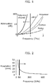
- FIG. 1 is a diagram illustrating the relationship between attenuation and frequency when electromagnetic waves transmit through a matter.
- electromagnetic waves having a frequency of at most 1 THz can transmit through many of matters used as materials for clothes, bags, or the like.
- the inventors have also studied on a frequency that achieves resolution with which the shape of a hazardous object can be imaged.
- Equation 1 ⁇ denotes resolution, ⁇ denotes the wavelength of electromagnetic waves, NA denotes the number of apertures of a lens, n denotes the refractive index of a medium between an object and the lens, and ⁇ denotes a maximum angle with respect to the optical axis of a light beam incident on the lens from the object.
- d the entrance pupil diameter of an imaging lens
- d the distance from the entrance pupil position of the imaging lens to the object
- sub-terahertz waves that are electromagnetic waves having a frequency that ranges from 0.08 THz to 1 THz, inclusive, in order to perform imaging that enables the detection of a hazardous object hidden, for instance, under people's clothes or the like, or in a bag.
- sub-terahertz waves do not affect human bodies. Therefore, utilizing sub-terahertz waves as electromagnetic waves to be emitted to a human body does not cause any problems in terms of safety.
- sub-terahertz waves specularly reflect off a human body, a metal, or the like. Therefore, in imaging utilizing electromagnetic waves (sub-terahertz waves in this case) emitted from a point light source, it is difficult to image, with high accuracy, the shape of a human body, or a metallic hazardous object such as a knife, as has conventionally been the case. In order to solve this problem, the inventors have studied on the shape of a light source that emits sub-terahertz waves.
- a light source that emits sub-terahertz waves is an area light source, it is possible to irradiate an object to be imaged with sub-terahertz waves from various angles, thereby enabling more accurate imaging, than that performed by a conventional imaging device, of the shape of an object such as a human body, a metal, or the like which specularly reflects sub-terahertz waves.
- An imaging device includes: an area light source including an emission surface from which a sub-terahertz wave is emitted to a measurement target; and a detector including an image sensor that receives a reflected wave generated by the measurement target reflecting the sub-terahertz wave emitted from the emission surface.
- the area light source includes: at least one point light source that emits a sub-terahertz wave; and a reflector that diffusely reflects the sub-terahertz wave emitted from the at least one point light source, to generate a sub-terahertz wave to be emitted from the emission surface, the reflector including a reflection surface that is a bumpy surface whose roughness curve element mean length RSm is at least 0.3 mm.
- the diffuse reflection here means that a ray of a sub-terahertz wave incident on the reflection surface at an angle of incidence when viewed at a macro level is reflected at multiple angles of reflection due to the structure of a bumpy surface having multiple bumps at a micro level.
- the imaging device utilizes sub-terahertz waves emitted from an area light source, to perform imaging. With the imaging device, it is therefore possible to image more accurately, than a conventional imaging device, the shape of an object such as a human body, a metal, or the like that is hidden under people's clothes or the like and cannot be visually identified directly.
- roughness curve element mean length RSm of the reflection surface is at least the wavelength of sub-terahertz waves. According to the imaging device described above, the generation of interference fringes in sub-terahertz waves emitted from the emission surface would be suppressed even if sub-terahertz waves emitted from each of at least one point light source were coherent electromagnetic waves.
- the detector may include an optical system that forms an image on the image sensor by an optical focus of the reflected wave.
- ⁇ denotes an entrance pupil diameter of the optical system
- b denotes a distance between the emission surface and the measurement target
- c denotes a distance between the measurement target and the optical system
- ⁇ denotes a wavelength of the sub-terahertz wave emitted from the at least one point light source
- the reflection surface may include one or more unit areas each of which has a bumpy surface including at least two frequency components in a frequency range of at most ( ⁇ ⁇ b / c) / ⁇ in a spatial frequency range
- a width of each of the one or more unit areas may be at least ⁇ ⁇ b / c
- the roughness curve element mean length RSm may be less than 2 ⁇ ⁇ ⁇ b / c.
- the one or more unit areas may include a first unit area and a second unit area.
- the first unit area and the second unit area may be in contact with each other at a side shared between the first unit area and the second unit area.
- a geometry of a bumpy surface of the first unit area and a geometry of a bumpy surface of the second unit area may be line symmetric about the side serving as an axis of symmetry.
- the detector may include an optical system that forms an image on the image sensor by an optical focus of the reflected wave.
- An angle ⁇ 1 that is a half width at half maximum of a strength of the sub-terahertz wave in the diffuse reflection by the reflector may be at least a value obtained using the following formula: tan ⁇ 1 a 2 b where a denotes a width of an imaging range of the measurement target and c denotes a distance between the measurement target and the optical system.
- the detector may include an optical system that forms an image on the image sensor by an optical focus of the reflected wave.
- An angle ⁇ 2 that is a half width at half maximum in a distribution of inclination angles of bumps on the reflection surface may be at least a value obtained using the following formula: 1 2 ⁇ tan ⁇ 1 a 2 b where a denotes a width of an imaging range of the measurement target and c denotes a distance between the measurement target and the optical system.
- planar surface refers not only to a surface that is accurately planar, but also to a surface that is substantially planar.
- spheroid refers not only to a surface that is accurately a spheroid, but also to a surface that is substantially a spheroid.
- the following describes an imaging device that emits sub-terahertz waves to a person, receives reflected waves generated by the person reflecting the sub-terahertz waves, and detects the intensity of the received reflected waves, to image a hazardous object such as a knife hidden by that person under his/her clothes or the like.
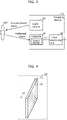
- FIG. 3 is a block diagram illustrating a configuration of imaging device 10 according to Embodiment 1.
- imaging device 10 includes light source 20, detector 30, and image processing unit 40.
- Light source 20 emits sub-terahertz waves to a measurement target (person 100 in this case).
- FIG. 4 is a schematic diagram illustrating a configuration of light source 20.
- light source 20 includes point light source 21 and optical element 23.
- Point light source 21 emits sub-terahertz waves radially in all directions in the vicinity of point light source 21.
- Optical element 23 has emission surface 22 and generates, from the sub-terahertz waves emitted from point light source 21, sub-terahertz waves to be emitted from emission surface 22.
- Emission surface 22 here is a planar surface. Therefore, optical element 23 functions as an area light source that emits sub-terahertz waves from emission surface 22 which is a planar surface.
- the emission surface from which sub-terahertz waves are emitted is a planar surface for the sake of explanation, but may be the inner surface of part of a spheroid to be described later, the inner surface of part of a sphere, or any curved surface.
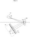
- FIG. 5 is a schematic diagram illustrating a cross section showing how light source 20 functions as an area light source that emits sub-terahertz waves and how detector 30 to be described later receives reflected waves generated by a measurement target.
- optical element 23 includes diffuser 24 and has a principal surface on its front side as emission surface 22.
- Diffuser 24 diffusely transmits the sub-terahertz waves emitted from point light source 21, to generate sub-terahertz waves to be emitted from emission surface 22.
- Diffuser 24 is a flat plate that is parallel to emission surface 22 when viewed from a macro perspective. When viewed from a micro perspective, on the other hand, tiny bumps are formed on the entire surface of diffuser 24 so that sub-terahertz waves diffuse when transmitting through diffuser 24.
- point light source 21 is disposed at the rear side of optical element 23, as illustrated in FIG. 5 .
- the sub-terahertz waves emitted from point light source 21 enter optical element 23 from the principal surface on the rear side of optical element 23 to reach diffuser 24.
- the sub-terahertz waves that have reached diffuser 24 diffusely transmit through diffuser 24.
- the sub-terahertz waves that have diffusely transmitted through diffuser 24 then propagate to emission surface 22 and are emitted outward from emission surface 22.
- imaging device 10 continues.
- Detector 30 includes image sensor 31.
- Image sensor 31 transforms an image generated by sub-terahertz waves emitted from a subject into an electric signal that is in accordance with the intensity of the sub-terahertz waves. Image sensor 31 then generates an image that is based on the electric signal into which the sub-terahertz waves are transformed.
- generating, by image sensor 31, an image including an image of a subject is also referred to as "imaging”.
- image sensor 31 receives the reflected waves.
- image sensor 31 receives reflected waves from an area, of the body of person 100 and the knife hidden by person 100, which is defined by an angle at which reflected waves resulting from the specular reflection are incident on image sensor 31.
- light source 20 functions as an area light source that emits sub-terahertz waves from emission surface 22. Therefore, light source 20 can irradiate person 100 with sub-terahertz waves from various angles. Image sensor 31 can thus receive reflected waves from area 101 that is a relatively wide range of the surfaces of person 100, i.e., the body of person 100, and a knife hidden by person 100. Accordingly, imaging device 10 is capable of imaging area 101 that is a relatively wide range of the surfaces of the body of person 100 and the knife hidden by person 100.
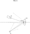
- FIG. 6 is a schematic diagram illustrating a cross section showing how detector 30 receives reflected waves in an imaging device according to a first comparative example, from which optical element 23 has been removed, that is, an imaging device configured to emit sub-terahertz waves emitted outward from point light source 21, as-is.
- image sensor 31 can receive only reflected waves from area 101a, of the surfaces of the body of person 100 and the knife hidden by person 100, which is defined by an angle at which reflected waves resulting from specular reflection are incident on image sensor 31, as illustrated in FIG. 6 . Accordingly, the imaging device according to the first comparative example can image only area 101a that is a relatively narrow area of the surfaces of the body of person 100 and the knife hidden by person 100.
- Detector 30 outputs an image generated by image sensor 31 to image processing unit 40.
- image processing unit 40 Upon receiving the image from detector 30, image processing unit 40 outputs the received image to an external device and also performs image processing on the received image and outputs the result of the image processing to the external device.
- the image processing performed by image processing unit 40 may be, for example, a process of determining whether an image outputted from detector 30 includes an object having predetermined characteristics (e.g., an object having the characteristics of a knife) and outputting a predetermined detection signal (e.g., an alarm indicating that an object having the characteristics of a knife is imaged) when it is determined that the image includes an object having the predetermined characteristics.
- Image processing unit 40 may include, for example, a processor and memory, and perform the process by the processor executing a program stored in the memory.
- Imaging device 10 having the above configuration is installed, for example, in a pathway at an airport, in the vicinity of an exit of a station, or the like.
- FIG. 7 is a schematic diagram illustrating how imaging device 10 is installed in a pathway at an airport.
- Imaging device 10 may be installed in such a manner, for example, that optical element 23 and detector 30 are embedded inside a wall along pathway 200 that is in a crank shape at an airport, as illustrated in FIG. 7 .
- sub-terahertz waves emitted from emission surface 22 inside the wall transmit through the wall and person 100 is irradiated with the sub-terahertz waves. Then, reflected waves generated by person 100 reflecting the sub-terahertz waves transmit through the wall again to be incident on detector 30. This enables imaging device 10 to image a hazardous object such as a knife hidden under the clothes or the like of person 100 walking along pathway 200.
- Embodiment 2 which has a configuration obtained by partly modifying the configuration of imaging device 10 according to Embodiment 1.
- the imaging device according to Embodiment 2 will be described mainly focusing on the difference between the imaging device according to Embodiment 2 and imaging device 10.
- FIG. 8 is a block diagram illustrating a configuration of imaging device 10a according to Embodiment 2.
- imaging device 10a includes first light source 20a and second light source 20b as modified from light source 20 of imaging device 10 according to Embodiment 1, first detector 30a and second detector 30b as modified from detector 30 of imaging device 10, and image processing unit 40a as modified from image processing unit 40 of imaging device 10.
- First light source 20a emits sub-terahertz waves to a measurement target (person 100 in this case).
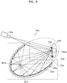
- FIG. 9 is a schematic diagram illustrating a configuration of first light source 20a as well as a cross section showing how first light source 20a functions as an area light source and how first detector 30a to be described later receives reflected waves.
- first light source 20a includes point light source 21a and optical element 23a.
- Point light source 21a emits sub-terahertz waves radially in all directions in the vicinity of point light source 21a.
- Optical element 23a has first emission surface 22a and generates, from the sub-terahertz waves emitted from point light source 21a, sub-terahertz waves to be emitted from first emission surface 22a.
- First emission surface 22a here is the inner surface of a spheroid. Therefore, optical element 23a functions as an area light source that emits sub-terahertz waves from first emission surface 22a which is the inner surface of a spheroid.
- optical element 23a includes reflector 24a and has first emission surface 22a as the inner curved surface of reflector 24a.
- Reflector 24a diffusely reflects sub-terahertz waves emitted from point light source 21a to generate sub-terahertz waves to be emitted from first emission surface 22a.
- reflector 24a has the same or larger size but is similar in shape compared to first emission surface 22a, and two focal points of reflector 24 match two focal points of first emission surface 22a.
- tiny bumps are formed on the entire surface of the reflection surface of reflector 24a so that the reflected sub-terahertz waves diffuse.
- first emission surface 22a and reflector 24a are separate components, first emission surface 22a and reflector 24a do not necessarily need to be limited to such an example of being separate components.
- first emission surface 22a may be the reflection surface of reflector 24a.
- Second light source 20b in FIG. 8 has the same function as that of first light source 20a, and has a shape that is in a mirrored relationship with the shape of first light source 20a. Therefore, second light source 20b can be explained by replacing point light source 21a with point light source 21b, optical element 23a with optical element 23b, reflector 24a with reflector 24b, one focal point 301a with one focal point 301b, and other focal point 302a with other focal point 302b in the description of first light source 20a, while keeping the description on the shape of second light source 20b unchanged.
- imaging device 10a continues.
- First detector 30a includes first image sensor 31a.
- First detector 30a is the same as detector 30 according to Embodiment 1.
- first image sensor 31a is the same as image sensor 31 according to Embodiment 1.
- Second detector 30b is the same as first detector 30a. Therefore, second detector 30b can be explained by reading first image sensor 31a as second image sensor 31b in the description of first detector 30a.
- first light source 20a functions as an area light source that emits sub-terahertz waves from first emission surface 22a.
- First light source 20a is therefore capable of irradiating person 100 in the vicinity of other focal point 302a with sub-terahertz waves from various angles.
- First image sensor 31a can thus receive reflected waves from area 102 that is a relatively wide range of the surfaces of person 100, that is, the body of person 100 and a knife hidden by person 100.
- imaging device 10a is capable of imaging area 102 that is a relatively wide range of the surfaces of the body of person 100 and the knife hidden by person 100.
- FIG. 10 is a schematic diagram illustrating a cross section showing how first detector 30a receives reflected waves in an imaging device according to a second comparative example which has a configuration in which reflector 24a of imaging device 10a is modified to reflector 24aa.
- reflector 24aa here has the same shape as reflector 24a, but when viewed from a micro perspective, the entire surface of the reflection surface of reflector 24aa is smoothly formed so that reflected sub-terahertz waves specularly reflect off the reflection surface.
- image sensor 31a can receive only reflected waves from area 102a, which is located at other focal point 302a, of the surfaces of the body of person 100 in the vicinity of other focal point 302a and the knife hidden under the clothes of person 100, as illustrated in FIG. 10 . Accordingly, the imaging device according to the second comparative example can image only area 102a that is a relatively narrow area of the surfaces of the body of person 100 and the knife hidden by person 100.
- imaging device 10a according to Embodiment 2 is capable of more accurately imaging the shapes of the body of person 100 and the knife hidden by person 100, as compared to the imaging device according to the second comparative example.
- imaging device 10a continues.
- First detector 30a and second detector 30b respectively output a first image and a second image respectively generated by first image sensor 31a and second image sensor 31b to image processing unit 40a.
- image processing unit 40a Upon receiving the first image and the second image from first detector 30a and second detector 30b, respectively, image processing unit 40a outputs the received first image and second image to an external device, and also performs image processing on the received first image and second image and outputs the result of the image processing to the external device.
- the image processing performed by image processing unit 40a may be, for example, determining whether the first image and the second image respectively outputted from first detector 30a and second detector 30b each include an object having predetermined characteristics (e.g., an object having the characteristics of a knife), and outputting a predetermined detection signal (e.g., an alarm indicating that an object having the characteristics of a knife is imaged) when it is determined that at least one of the first image or the second image includes an object having predetermined characteristics.
- a predetermined detection signal e.g., an alarm indicating that an object having the characteristics of a knife is imaged
- the image processing performed by image processing unit 40a may also include a process of: blending the first image and the second image in a lighten only mode to generate a blended image in the case where it is determined that at least one of the first image or the second image includes an object having the predetermined characteristics; determining whether the blended image includes an object having the predetermined characteristics; and in the case where it is determined that the blended image includes an object having the predetermined characteristics, outputting a predetermined detection signal.
- Image processing unit 40a may include, for example, a processor and memory, and perform the process by the processor executing a program stored in the memory.
- Imaging device 10a having the above configuration is installed, for example, in a pathway at an airport or in the vicinity of an exit of a station.
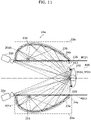
- FIG. 11 is a schematic diagram illustrating a cross section showing how imaging device 10a is installed in a pathway in the vicinity of an exit of a station.
- Imaging device 10a may be installed in such a manner, for example, that optical element 23a and optical element 23b are embedded inside walls along pathway 400 in the vicinity of an exit of a station, as illustrated in FIG. 11 . More specifically, imaging device 10a may be installed in such a manner, for example, that optical element 23a is embedded inside wall 401a that is one of the side walls along pathway 400 and optical element 23b is embedded inside wall 401b that is the other of the side walls along pathway 400. Thus, imaging device 10a may be installed in such a manner that first light source 20a and second light source 20b are provided on opposite sides of pathway 400 and first detector 30a and second detector 30b are also provided on opposite sides of pathway 400.
- first detector 30a detects, using first image sensor 31a, the intensities of reflected waves generated by a measurement target (person 100 in this case) positioned in pathway 400 reflecting sub-terahertz waves emitted from first emission surface 22a and sub-terahertz waves emitted from second emission surface 22b
- second detector 30b detects, using second image sensor 31b, the intensities of reflected waves generated by a measurement target (person 100 in this case) positioned in pathway 400 reflecting sub-terahertz waves emitted from first emission surface 22a and sub-terahertz waves emitted from second emission surface 22b.
- optical element 23a and optical element 23b be installed so that other focal point 302a of optical element 23a substantially coincides with other focal point 302b of optical element 23b on the center line of pathway 400.
- focal area an area in the vicinity of other focal point 302a or other focal point 302b (hereinafter referred to as "focal area") with sub-terahertz waves emitted from point light source 21a and sub-terahertz waves emitted from point light source 21b from various angles.
- first image sensor 31a and second image sensor 31b respectively included in first detector 30a and second detector 30b can receive reflected waves from area 103 that is a relatively wide range of the surface of person 100 walking in the focal area, that is, the body of person 100 walking in a focal area and the surface of the knife hidden by person 100, as illustrated in FIG. 11 .
- imaging device 10a is capable of imaging area 103 that is a relatively wide range of the surfaces of the body of person 100 and the knife hidden by person 100.
- first image sensor 31a and second image sensor 31b respectively included in first detector 30a and second detector 30b receive reflected waves from mutually different angles from area 103.
- imaging device 10a is capable of imaging the body of person 100 and the knife hidden by person 100, which are the same subject, from mutually different angles.
- imaging device 10a having the above configuration will be described.
- imaging device 10a performs an image analysis process.
- the image analysis process is a process in which imaging device 10a images a first image and a second image and outputs, based on the imaged first image and second image, a detection signal which is an alarm indicating that an object having the characteristics of a knife is being imaged.
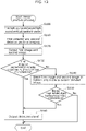
- FIG. 12 is a flowchart illustrating the image analysis process performed by imaging device 10a.
- the image analysis process is started when a person enters a focal area.
- imaging device 10a When a person enters a focal area, imaging device 10a detects that the person has entered the focal area. Imaging device 10a may detect that a person has entered the focal area, for example, by receiving a signal indicating that the person has entered the focal area from an external sensor that detects a person entering the focal area.
- first light source 20a and second light source 20b emit sub-terahertz waves at the same timing in synchronization with each other (step S100).
- first detector 30a and second detector 30b image the person having entered the focal area at the timing when first light source 20a and second light source 20b emit the sub-terahertz waves in synchronization with each other (step S110).
- First detector 30a and second detector 30b then respectively output a first image and a second image to image processing unit 40a.
- image processing unit 40a receives the first image and the second image that have been output and outputs the received first image and second image to an external device (step S120). Image processing unit 40a then determines whether at least one of the first image or the second image includes an object having the characteristics of a knife which are predetermined characteristics (step S130).
- step S130 in the case of not determining that at least one of the first image or the second image includes an object having the predetermined characteristics (step S130: No), image processing unit 40a blends the first image and the second image in a lighten only mode to generate a blended image, and outputs the generated blended image (step S140). Image processing unit 40a then determines whether the generated blended image includes an object having the characteristics of a knife which are the predetermined characteristics (step S150).
- image processing unit 40a In the case of determining that at least one of the first image or the second image includes an object having the predetermined characteristics (step S130: Yes) in the process of step S130 and also in the case of determining that the blended image includes an object having the predetermined characteristics (step S150: Yes) in the process of step S150, image processing unit 40a outputs, to an external device, a detection signal which is an alarm indicating that an object having the characteristics of a knife is being imaged (step S160).
- Imaging device 10a ends the image analysis process when the process of step S160 ends or in the case of not determining that the blended image includes an object including the predetermined characteristics (step S150: No) in the process of step S150.
- Imaging device resulting from modifying part of the configuration of imaging device 10a according to Embodiment 2 will be described.
- the imaging device according to Embodiment 3 will be described focusing on the difference from imaging device 10a.
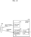
- FIG. 13 is a block diagram illustrating the configuration of imaging device 10b according to Embodiment 3.
- imaging device 10b is configured as a result of removing second light source 20b and second detector 30b from imaging device 10a according to Embodiment 2, and replacing first detector 30a with detector 30c and image processing unit 40a with image processing unit 40b.
- Detector 30c includes image sensor 31 and optical system 32.
- Optical system 32 forms an image by the optical focus of reflected waves generated by a measurement target (person 100 in this case) reflecting sub-terahertz waves emitted from first emission surface 22a.
- Optical system 32 includes at least one lens including lens 33.
- ⁇ denotes the entrance pupil diameter of optical system 32.
- Detector 30c outputs an image generated by image sensor 31 to image processing unit 40b.
- image processing unit 40b Upon receiving the image from detector 30c, image processing unit 40b outputs the received image to an external device as well as performs image processing on the received image and outputs the result of the image processing to the external device.
- the image processing performed by image processing unit 40b is the same processing as the image processing performed by image processing unit 40 according to Embodiment 1.
- the reflection surface of reflector 24a has a bumpy surface whose roughness curve element mean length RSm is at least 0.3 mm.
- the wavelength of sub-terahertz waves emitted from point light source 21a is at most 0.3 mm. Accordingly, the sub-terahertz waves emitted from point light source 21a are diffusely reflected when irradiated on the reflection surface that is a bumpy surface whose roughness curve element mean length RSm is at least 0.3 mm. Thus, owing to the reflection surface of reflector 24a being a bumpy surface whose roughness curve element mean length RSm is at least the wavelength of sub-terahertz waves, the diffuse reflection of the sub-terahertz waves emitted from point light source 21a is achieved.
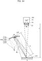
- FIG. 14 is a schematic diagram illustrating how imaging device 10b images a measurement target.
- imaging range 110 is an area to be subjected to imaging by imaging device 10b out of the surface of the measurement target. As described in Embodiment 2, imaging range 110 is an area in the vicinity of other focal point 302a (see, for example, FIG. 9 ) out of the two focal points of first emission surface 22a. On the other hand, point light source 21a is located at one focal point 301a (see, for example, FIG. 9 ) out of the two focal points of first emission surface 22a.
- Imaging sub-terahertz wave emission area 120 is an area that is a portion of first emission surface 22a, and is an area from which sub-terahertz waves, which are the origin of reflected light components that form an image on image sensor 31, are emitted out of reflected light reflected by the measurement target.
- Distance b is the distance between first emission surface 22a and the measurement target. More specifically, distance b is the distance between imaging sub-terahertz wave emission area 120 and imaging range 110.
- Distance c is the distance between the measurement target and optical system 32. More specifically, distance c is the distance between imaging range 110 and optical system 32.
- interference fringes may occur in the reflected light by the focus of which an image is formed on image sensor 31.
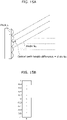
- FIG. 15A is a schematic diagram illustrating how the reflection surface of a reflector according to a comparative example reflects sub-terahertz waves.
- an emission surface according to the comparative example has a periodic structure composed of pitches d.
- FIG. 15B is a schematic diagram illustrating how the sub-terahertz waves reflected by the reflection surface of the reflector according to the comparative example generate interference fringes.
- the reflection surface of reflector 24a in imaging sub-terahertz wave emission area 120 has a periodic structure composed of only one frequency component of ⁇ '/d in a spatial frequency range, if sub-terahertz waves emitted from point light source 21a are coherent sub-terahertz waves, an image formed on image sensor 31 receives a relatively large influence from interference fringes.
- the actual reflection surface of reflector 24a is a bumpy surface including at least two frequency components in the frequency range of at most ⁇ '/ ⁇ in the spatial frequency range when ⁇ denotes the wavelength of sub-terahertz waves emitted from point light source 21a.
- FIG. 15C is an enlarged cross-sectional view of an example of the actual reflection surface of reflector 24a.
- the reflection surface of reflector 24a is a bumpy surface where spatial frequencies include 1 to 5 with the same strength in the spatial frequency range.
- the reflection surface of reflector 24a be a bumpy surface in a random form in terms of reducing the influence of interference fringes on the image of a measurement target formed on image sensor 31.
- the reflection surface of reflector 24a has unit areas each of which has the width of at least ⁇ ⁇ b / c.
- Each of the unit areas is described herein as an area whose shape viewed along a direction perpendicular to the tangent plane of a spheroid in the macro perspective of the reflection surface is an approximate rectangle.
- the width of a unit area is a shorter distance out of the distance between longer sides facing each other and the distance between shorter sides facing each other of the unit area that is an approximate rectangle.
- FIG. 16A is a plan view of unit areas 500 (i.e., unit area 500a to unit area 500d) included in the reflection surface of reflector 24a when viewed along a direction perpendicular to the tangent plane of a spheroid in the macro perspective of the reflection surface.
- a location at which each tangent plane comes in contact with the spheroid is at the center of a corresponding one of rectangles illustrated as unit area 500a to unit area 500d in FIG. 16A .
- Each of unit areas 500 is composed of a bumpy surface that includes at least two frequency components in the frequency range of at most ⁇ '/ ⁇ in a spatial frequency range when ⁇ denotes the wavelength of sub-terahertz waves emitted from point light source 21a.
- FIG. 16B is a schematic diagram illustrating how unit areas 500 are arranged on the reflection surface of reflector 24a.
- unit area 500a and unit area 500b share, as a side, side 501a of unit area 500a and side 501b of unit area 500b, and are disposed in contact with each other at the side, as illustrated in FIG. 16A and FIG. 16B .
- the geometry of the bumpy surface of unit area 500a and the geometry of the bumpy surface of unit area 500b are line symmetric about the side serving as an axis of symmetry.
- unit area 500a and unit area 500c share, as a side, side 502a of unit area 500a and side 502c of unit area 500c, and are disposed in contact with each other at the side.
- the geometry of the bumpy surface of unit area 500a and the geometry of the bumpy surface of unit area 500c are line symmetric about the side serving as an axis of symmetry.
- unit area 500b and unit area 500d share, as a side, side 502b of unit area 500b and side 502d of unit area 500d, and are disposed in contact with each other at the side.
- the geometry of the bumpy surface of unit area 500b and the geometry of the bumpy surface of unit area 500d are line symmetric about the side serving as an axis of symmetry.
- unit area 500c and unit area 500d share, as a side, side 501c of unit area 500c and side 501d of unit area 500d, and are disposed in contact with each other at the side.
- the geometry of the bumpy surface of unit area 500c and the geometry of the bumpy surface of unit area 500d are line symmetric about the side serving as an axis of symmetry.
- Unit area 500a to unit area 500d are thus arranged on the entire reflection surface of reflector 24a without any space left, as illustrated in FIG. 16B .
- the reflection surface of reflector 24a achieves, for any area whose width is ⁇ ', a bumpy surface that includes at least two frequency components in the frequency range of at most ⁇ '/ ⁇ in a spatial frequency range when ⁇ denotes the wavelength of sub-terahertz waves emitted from point light source 21a.
- imaging device 10b continues.
- angle ⁇ 1 denotes an angle that is the half width at half maximum of the strength of sub-terahertz waves in diffuse reflection at any location on reflector 24a.
- imaging range 110 is located within the range of angle ⁇ 1.
- angle ⁇ 1 satisfies Expression 5 indicated below.
- FIG. 17 is a schematic diagram illustrating a cross section of an inclined portion of a bump on the reflection surface of reflector 24a.
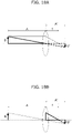
- FIG. 18A and FIG. 18B are schematic diagrams each illustrating the relationship between a subject and the actual image of the subject in optical system 32.
- focal distance f is the focal distance of optical system 32
- distance A is the distance from optical system 32 to the subject
- height B is the height of the subject
- distance A' is the distance from optical system 32 to the actual image of the subject formed by optical system 32
- height B is the height of the actual image.
- Equation 7 indicated below holds true based on the fact that a triangle in a thick solid line is similar to a triangle in a thick dashed line in FIG. 18A .
- a : A ′ B : B ′
- Equation 8 indicated below holds true based on the fact that a triangle in a thick solid line is similar to a triangle in a thick dashed line in FIG. 18B .
- B : B ′ f : A ′ ⁇ f
- a ′ f ⁇ A / A ⁇ f
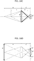
- FIG. 18C and FIG. 18D are schematic diagrams each illustrating how dots located in imaging sub-terahertz wave emission area 120 form an image on image sensor 31 by optical system 32.
- distance c is the distance between imaging range 110 and optical system 32
- distance e is the distance between imaging sub-terahertz wave emission area 120 and optical system 32, that is, a sum of distance c and distance b which is the distance between imaging sub-terahertz wave emission area 120 and imaging range 110
- distance c' is the distance between optical system 32 and image sensor 31
- distance e' is the distance between optical system 32 and the location at which dots located in imaging sub-terahertz wave emission area 120 form an image
- width ⁇ " is the width of the image, which is formed on image sensor 31, of the dots located in imaging sub-terahertz wave emission area 120, that is, a width showing the spread of the blurred image, which is formed on image sensor 31, of the dots located in imaging sub-terahertz wave emission area 120.
- length P is roughness curve element mean length RSm of the reflection surface of reflector 24a
- height P' is the height of the actual image of a subject with height P at the location of first emission surface 22a, that is, a subject whose height is roughness curve element mean length RSm of the reflection surface of reflector 24a.
- Equation 11 and Equation 12 indicated below hold true based on Equation 9.
- roughness curve element mean length RSm of the reflection surface of reflector 24a be less than 2 ⁇ ⁇ ⁇ b/ c so that the structure of the bumpy surface that is the reflection surface of reflector 24a does not resolve an image.
- the imaging device has been described based on Embodiment 1 or Embodiment 2, but the present disclosure is not limited to these embodiments.
- Various modifications to the embodiments which may be conceived by those skilled in the art, as well as embodiments resulting from arbitrary combinations of elements from different embodiments may be included within the scope of one or more aspects of the present disclosure so long as they do not depart from the essence of the present disclosure.
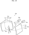
- FIG. 19 is a schematic diagram illustrating part of an outer appearance of the imaging device according to the variation.
- first light source 20c according to the variation includes point light source 21a and optical element 23c having first emission surface 22c which is the inner surface of part of a sphere, as illustrated in FIG. 19 .
- Point light source 21a is disposed in the vicinity of the center of the sphere.
- Second light source 20d according to the variation includes point light source 21b and optical element 23d having second emission surface 22d which is the inner surface of part of the sphere.
- Point light source 21b is disposed in the vicinity of the center of the sphere.
- optical element 23 includes diffuser 24.
- optical element 23 may be diffuser 24 per se, as another example.
- the surface of diffuser 24 is emission surface 22.
- optical element 23a and optical element 23b include reflector 24a and reflector 24b, respectively.
- optical element 23a and optical element 23b may be reflector 24a per se and reflector 24b per se, respectively.
- the reflection surface of reflector 24a and the reflection surface of reflector 24b are first emission surface 22a and second emission surface 22b, respectively.
- Embodiment 1 has described that light source 20 includes one point light source 21.
- the number of point light sources included in light source 20 does not need to be limited to one and may be plural.
- optical element 23 generates, from sub-terahertz waves emitted from a plurality of point light sources, sub-terahertz waves to be emitted from emission surface 22.
- first light source 20a and second light source 20b respectively include one point light source 21a and one point light source 21b.
- the number of point light sources included in first light source 20a or second light source 20b does not need to be limited to one and may be plural.
- optical element 23a and optical element 23b generate, from sub-terahertz waves emitted from a plurality of point light sources, sub-terahertz waves to be emitted from first emission surface 22a and sub-terahertz waves to be emitted from second emission surface 22b, respectively.
- Embodiment 2 has described that first emission surface 22a and second emission surface 22b are each the inner surface of a spheroid.
- First emission surface 22a and second emission surface 22b are not necessarily limited to an example where first emission surface 22a and second emission surface 22b are each the inner surface of a spheroid in an accurate sense, and may be, for example, a polyhedron composed of multiple micro-polygons approximated to a spheroid.
- each of one or more unit areas 500 is an approximate rectangle when viewed along a direction perpendicular to the tangent plane of a spheroid in the macro perspective of the reflection surface of reflector 24a.
- Each of one or more unit areas 500 does not necessarily need to be an approximate rectangle so long as unit area 500 can cover the entire reflection surface of reflector 24a without any space left.
- each of one or more unit areas 500 may be an approximate regular hexagon when viewed along a direction perpendicular to the tangent plane of a spheroid in the macro perspective of the reflection surface of reflector 24a.
- the width of a unit area is the distance between sides of the approximate regular hexagon which face each other.
- An aspect of the present disclosure may be not only the imaging device according to Embodiment 1 to Embodiment 3, but also an imaging method implementing steps performed by characteristic components included in the imaging device.
- an aspect of the present disclosure may be a program causing a computer to execute each of the characteristic steps included in the imaging method.
- an aspect of the present disclosure may be a non-transitory computer-readable recording medium having such a program recorded thereon.
- the present disclosure can be widely used for imaging devices that image objects.
Landscapes
- Physics & Mathematics (AREA)
- Spectroscopy & Molecular Physics (AREA)
- General Physics & Mathematics (AREA)
- Engineering & Computer Science (AREA)
- Electromagnetism (AREA)
- Remote Sensing (AREA)
- Radar, Positioning & Navigation (AREA)
- Computer Networks & Wireless Communication (AREA)
- Health & Medical Sciences (AREA)
- Biochemistry (AREA)
- Immunology (AREA)
- Pathology (AREA)
- Toxicology (AREA)
- General Health & Medical Sciences (AREA)
- Life Sciences & Earth Sciences (AREA)
- Analytical Chemistry (AREA)
- Chemical & Material Sciences (AREA)
- Optics & Photonics (AREA)
- Investigating Or Analysing Materials By Optical Means (AREA)
Applications Claiming Priority (2)
| Application Number | Priority Date | Filing Date | Title |
|---|---|---|---|
| JP2020048096 | 2020-03-18 | ||
| PCT/JP2020/047117 WO2021186822A1 (fr) | 2020-03-18 | 2020-12-17 | Dispositif photographique |
Publications (2)
| Publication Number | Publication Date |
|---|---|
| EP4123271A1 true EP4123271A1 (fr) | 2023-01-25 |
| EP4123271A4 EP4123271A4 (fr) | 2023-07-26 |
Family
ID=77771913
Family Applications (1)
| Application Number | Title | Priority Date | Filing Date |
|---|---|---|---|
| EP20925147.9A Withdrawn EP4123271A4 (fr) | 2020-03-18 | 2020-12-17 | Dispositif photographique |
Country Status (5)
| Country | Link |
|---|---|
| US (1) | US12259320B2 (fr) |
| EP (1) | EP4123271A4 (fr) |
| JP (1) | JP7645452B2 (fr) |
| CN (1) | CN115280098A (fr) |
| WO (1) | WO2021186822A1 (fr) |
Families Citing this family (1)
| Publication number | Priority date | Publication date | Assignee | Title |
|---|---|---|---|---|
| EP4123271A4 (fr) * | 2020-03-18 | 2023-07-26 | Panasonic Intellectual Property Management Co., Ltd. | Dispositif photographique |
Family Cites Families (29)
| Publication number | Priority date | Publication date | Assignee | Title |
|---|---|---|---|---|
| US5517575A (en) * | 1991-10-04 | 1996-05-14 | Ladewski; Theodore B. | Methods of correcting optically generated errors in an electro-optical gauging system |
| GB9700966D0 (en) * | 1997-01-17 | 1997-03-05 | Secr Defence | Millimetre wave imaging apparatus |
| FI107407B (fi) * | 1997-09-16 | 2001-07-31 | Metorex Internat Oy | Alimillimetriaalloilla toimiva kuvausjärjestelmä |
| US6777684B1 (en) * | 1999-08-23 | 2004-08-17 | Rose Research L.L.C. | Systems and methods for millimeter and sub-millimeter wave imaging |
| JP2002258272A (ja) * | 2001-02-28 | 2002-09-11 | Nec Corp | 反射板並びに反射型液晶表示装置 |
| US20090240139A1 (en) * | 2008-03-18 | 2009-09-24 | Steven Yi | Diffuse Optical Tomography System and Method of Use |
| JP5291983B2 (ja) * | 2008-05-12 | 2013-09-18 | 浜松ホトニクス株式会社 | テラヘルツ波周波数分解イメージング装置 |
| US8497477B1 (en) | 2010-02-10 | 2013-07-30 | Mvt Equity Llc | Method and apparatus for efficient removal of gain fluctuation effects in passive thermal images |
| US9086483B2 (en) * | 2011-03-28 | 2015-07-21 | Northrop Grumman Guidance And Electronics Company, Inc. | Systems and methods for detecting and/or identifying materials |
| US9207317B2 (en) * | 2011-04-15 | 2015-12-08 | Ariel-University Research And Development Company Ltd. | Passive millimeter-wave detector |
| US9268017B2 (en) * | 2011-07-29 | 2016-02-23 | International Business Machines Corporation | Near-field millimeter wave imaging |
| DE102012003201A1 (de) * | 2012-02-17 | 2013-08-22 | Hübner GmbH | Verfahren und Vorrichtung zur Untersuchung von Postsendungen im Hinblick auf gefährliche Inhaltsstoffe |
| JP2014029478A (ja) * | 2012-07-03 | 2014-02-13 | Canon Inc | テラヘルツ波発生素子、テラヘルツ波検出素子、及びテラヘルツ時間領域分光装置 |
| JP6290036B2 (ja) * | 2013-09-25 | 2018-03-07 | 株式会社東芝 | 検査装置及び検査システム |
| WO2015050941A1 (fr) * | 2013-10-04 | 2015-04-09 | Battelle Memorial Institute | Fantôme de contraste pour systèmes d'imagerie à longueur d'onde millimétrique passifs |
| MX361644B (es) * | 2013-12-24 | 2018-12-13 | Halliburton Energy Services Inc | Monitorización en tiempo real de la fabricación de elementos computacionales integrados. |
| WO2015101921A1 (fr) * | 2013-12-30 | 2015-07-09 | University Of Manitoba | Imagerie utilisant des éléments à grille |
| JP6490439B2 (ja) * | 2015-02-05 | 2019-03-27 | 国立研究開発法人情報通信研究機構 | 電波反射体 |
| JP2017009296A (ja) * | 2015-06-16 | 2017-01-12 | キヤノン株式会社 | 電磁波伝搬装置及び情報取得装置 |
| JP6778856B2 (ja) * | 2016-03-25 | 2020-11-04 | パナソニックIpマネジメント株式会社 | ミラーパネル、ミラーフィルム及び表示システム |
| US11385105B2 (en) * | 2016-04-04 | 2022-07-12 | Teledyne Flir, Llc | Techniques for determining emitted radiation intensity |
| JP6843600B2 (ja) * | 2016-11-28 | 2021-03-17 | キヤノン株式会社 | 画像取得装置、これを用いた画像取得方法及び照射装置 |
| JP6916435B2 (ja) * | 2017-01-17 | 2021-08-11 | 澁谷工業株式会社 | テラヘルツ光発生装置 |
| US10585185B2 (en) * | 2017-02-03 | 2020-03-10 | Rohde & Schwarz Gmbh & Co. Kg | Security scanning system with walk-through-gate |
| EP3613150A4 (fr) * | 2017-04-20 | 2020-12-02 | The Board of Trustees of the Leland Stanford Junior University | Réseaux extensibles à ondes millimétriques ayant de grandes ouvertures réalisées par des guides d'ondes diélectriques à ondes millimétriques |
| CN108444913A (zh) * | 2018-01-30 | 2018-08-24 | 中国科学院上海技术物理研究所 | 基于单元胞立体相位光栅和互参考技术的THz光谱仪 |
| CA3090636A1 (fr) * | 2019-08-23 | 2021-02-23 | Institut National D'optique | Source d'illumination terahertz pour une imagerie terahertz |
| WO2021070428A1 (fr) | 2019-10-09 | 2021-04-15 | パナソニックIpマネジメント株式会社 | Dispositif de photographie |
| EP4123271A4 (fr) * | 2020-03-18 | 2023-07-26 | Panasonic Intellectual Property Management Co., Ltd. | Dispositif photographique |
-
2020
- 2020-12-17 EP EP20925147.9A patent/EP4123271A4/fr not_active Withdrawn
- 2020-12-17 JP JP2022508065A patent/JP7645452B2/ja active Active
- 2020-12-17 CN CN202080098553.9A patent/CN115280098A/zh active Pending
- 2020-12-17 WO PCT/JP2020/047117 patent/WO2021186822A1/fr not_active Ceased
-
2022
- 2022-09-08 US US17/940,372 patent/US12259320B2/en active Active
Also Published As
| Publication number | Publication date |
|---|---|
| JP7645452B2 (ja) | 2025-03-14 |
| US20230003643A1 (en) | 2023-01-05 |
| US12259320B2 (en) | 2025-03-25 |
| WO2021186822A1 (fr) | 2021-09-23 |
| CN115280098A (zh) | 2022-11-01 |
| JPWO2021186822A1 (fr) | 2021-09-23 |
| EP4123271A4 (fr) | 2023-07-26 |
Similar Documents
| Publication | Publication Date | Title |
|---|---|---|
| US20220224845A1 (en) | Imaging device | |
| CN102253392B (zh) | 飞行时间摄像机单元和光学监视系统 | |
| US8144327B2 (en) | Photoacoustic apparatus, and probe for receiving photoacoustic waves | |
| US20150133765A1 (en) | Biological information acquisition apparatus | |
| US20120179022A1 (en) | Bioinformation acquisition apparatus | |
| US20070114418A1 (en) | Security portal with THz trans-receiver | |
| EP2975447A1 (fr) | Scanner laser | |
| EP3737909B1 (fr) | Appareil de détection et système embarqué le comprenant | |
| EP4170319A1 (fr) | Dispositif de photographie | |
| US12259320B2 (en) | Imaging device | |
| CN104833315A (zh) | 光学探测器、可装配盖和形状测量设备 | |
| US20030081428A1 (en) | Device and method for uniform contact illumination | |
| CN105074430A (zh) | 成像系统 | |
| KR20240043339A (ko) | 은닉된 위험물을 탐지하는 보안검색기 | |
| JP7462354B2 (ja) | 組織成分の非侵襲検出方法、装置、システム及びウェアラブルデバイス | |
| JP7733996B2 (ja) | イメージング装置 | |
| CN104833316A (zh) | 光学探测器、可装配盖和形状测量设备 | |
| RU2812583C1 (ru) | Способ, устройство, система и носимое устройство неинвазивного детектирования для элемента ткани | |
| JP7311718B2 (ja) | 測距装置 | |
| JP7746105B2 (ja) | カメラシステム | |
| EP4597082A1 (fr) | Dispositif d'acquisition d'images, dispositif d'inspection et procédé d'acquisition d'images | |
| JP2021069857A (ja) | 測定装置 | |
| EP3575777A1 (fr) | Appareil de détermination de la fonction de distribution de réflexion bidirectionelle utilisant un motif d'éclairage asymétrique | |
| JP6481435B2 (ja) | 光学デバイス | |
| US20230116330A1 (en) | Imaging apparatus |
Legal Events
| Date | Code | Title | Description |
|---|---|---|---|
| STAA | Information on the status of an ep patent application or granted ep patent |
Free format text: STATUS: THE INTERNATIONAL PUBLICATION HAS BEEN MADE |
|
| PUAI | Public reference made under article 153(3) epc to a published international application that has entered the european phase |
Free format text: ORIGINAL CODE: 0009012 |
|
| STAA | Information on the status of an ep patent application or granted ep patent |
Free format text: STATUS: REQUEST FOR EXAMINATION WAS MADE |
|
| 17P | Request for examination filed |
Effective date: 20220905 |
|
| AK | Designated contracting states |
Kind code of ref document: A1 Designated state(s): AL AT BE BG CH CY CZ DE DK EE ES FI FR GB GR HR HU IE IS IT LI LT LU LV MC MK MT NL NO PL PT RO RS SE SI SK SM TR |
|
| DAV | Request for validation of the european patent (deleted) | ||
| DAX | Request for extension of the european patent (deleted) | ||
| A4 | Supplementary search report drawn up and despatched |
Effective date: 20230626 |
|
| RIC1 | Information provided on ipc code assigned before grant |
Ipc: G01N 22/00 20060101ALI20230620BHEP Ipc: G01N 21/3581 20140101ALI20230620BHEP Ipc: G01J 3/42 20060101ALI20230620BHEP Ipc: G01J 3/10 20060101ALI20230620BHEP Ipc: G01J 3/02 20060101ALI20230620BHEP Ipc: G01S 17/04 20200101ALI20230620BHEP Ipc: G01S 17/00 20200101ALI20230620BHEP Ipc: G01S 17/87 20200101ALI20230620BHEP Ipc: G02B 5/02 20060101ALI20230620BHEP Ipc: G01B 15/04 20060101ALI20230620BHEP Ipc: G01J 1/02 20060101AFI20230620BHEP |
|
| STAA | Information on the status of an ep patent application or granted ep patent |
Free format text: STATUS: THE APPLICATION IS DEEMED TO BE WITHDRAWN |
|
| 18D | Application deemed to be withdrawn |
Effective date: 20240124 |