EP4123697A1 - Carte de circuit isolée - Google Patents
Carte de circuit isolée Download PDFInfo
- Publication number
- EP4123697A1 EP4123697A1 EP21772541.5A EP21772541A EP4123697A1 EP 4123697 A1 EP4123697 A1 EP 4123697A1 EP 21772541 A EP21772541 A EP 21772541A EP 4123697 A1 EP4123697 A1 EP 4123697A1
- Authority
- EP
- European Patent Office
- Prior art keywords
- bonding interface
- aluminum sheet
- ceramic substrate
- bonding
- insulating circuit
- Prior art date
- Legal status (The legal status is an assumption and is not a legal conclusion. Google has not performed a legal analysis and makes no representation as to the accuracy of the status listed.)
- Pending
Links
Images



Classifications
-
- C—CHEMISTRY; METALLURGY
- C04—CEMENTS; CONCRETE; ARTIFICIAL STONE; CERAMICS; REFRACTORIES
- C04B—LIME, MAGNESIA; SLAG; CEMENTS; COMPOSITIONS THEREOF, e.g. MORTARS, CONCRETE OR LIKE BUILDING MATERIALS; ARTIFICIAL STONE; CERAMICS; REFRACTORIES; TREATMENT OF NATURAL STONE
- C04B37/00—Joining burned ceramic articles with other burned ceramic articles or other articles by heating
- C04B37/02—Joining burned ceramic articles with other burned ceramic articles or other articles by heating with metallic articles
- C04B37/023—Joining burned ceramic articles with other burned ceramic articles or other articles by heating with metallic articles characterised by the interlayer used
- C04B37/026—Joining burned ceramic articles with other burned ceramic articles or other articles by heating with metallic articles characterised by the interlayer used consisting of metals or metal salts
-
- H—ELECTRICITY
- H05—ELECTRIC TECHNIQUES NOT OTHERWISE PROVIDED FOR
- H05K—PRINTED CIRCUITS; CASINGS OR CONSTRUCTIONAL DETAILS OF ELECTRIC APPARATUS; MANUFACTURE OF ASSEMBLAGES OF ELECTRICAL COMPONENTS
- H05K3/00—Apparatus or processes for manufacturing printed circuits
- H05K3/0058—Laminating printed circuit boards onto other substrates, e.g. metallic substrates
- H05K3/0061—Laminating printed circuit boards onto other substrates, e.g. metallic substrates onto a metallic substrate, e.g. a heat sink
-
- H—ELECTRICITY
- H10—SEMICONDUCTOR DEVICES; ELECTRIC SOLID-STATE DEVICES NOT OTHERWISE PROVIDED FOR
- H10W—GENERIC PACKAGES, INTERCONNECTIONS, CONNECTORS OR OTHER CONSTRUCTIONAL DETAILS OF DEVICES COVERED BY CLASS H10
- H10W70/00—Package substrates; Interposers; Redistribution layers [RDL]
- H10W70/60—Insulating or insulated package substrates; Interposers; Redistribution layers
- H10W70/62—Insulating or insulated package substrates; Interposers; Redistribution layers characterised by their interconnections
- H10W70/65—Shapes or dispositions of interconnections
-
- H—ELECTRICITY
- H05—ELECTRIC TECHNIQUES NOT OTHERWISE PROVIDED FOR
- H05K—PRINTED CIRCUITS; CASINGS OR CONSTRUCTIONAL DETAILS OF ELECTRIC APPARATUS; MANUFACTURE OF ASSEMBLAGES OF ELECTRICAL COMPONENTS
- H05K1/00—Printed circuits
- H05K1/02—Details
- H05K1/0201—Thermal arrangements, e.g. for cooling, heating or preventing overheating
- H05K1/0203—Cooling of mounted components
- H05K1/0204—Cooling of mounted components using means for thermal conduction connection in the thickness direction of the substrate
-
- H—ELECTRICITY
- H10—SEMICONDUCTOR DEVICES; ELECTRIC SOLID-STATE DEVICES NOT OTHERWISE PROVIDED FOR
- H10W—GENERIC PACKAGES, INTERCONNECTIONS, CONNECTORS OR OTHER CONSTRUCTIONAL DETAILS OF DEVICES COVERED BY CLASS H10
- H10W40/00—Arrangements for thermal protection or thermal control
- H10W40/10—Arrangements for heating
-
- H—ELECTRICITY
- H10—SEMICONDUCTOR DEVICES; ELECTRIC SOLID-STATE DEVICES NOT OTHERWISE PROVIDED FOR
- H10W—GENERIC PACKAGES, INTERCONNECTIONS, CONNECTORS OR OTHER CONSTRUCTIONAL DETAILS OF DEVICES COVERED BY CLASS H10
- H10W70/00—Package substrates; Interposers; Redistribution layers [RDL]
- H10W70/60—Insulating or insulated package substrates; Interposers; Redistribution layers
- H10W70/62—Insulating or insulated package substrates; Interposers; Redistribution layers characterised by their interconnections
- H10W70/65—Shapes or dispositions of interconnections
- H10W70/657—Shapes or dispositions of interconnections on sidewalls or bottom surfaces of the package substrates, interposers or redistribution layers
-
- C—CHEMISTRY; METALLURGY
- C04—CEMENTS; CONCRETE; ARTIFICIAL STONE; CERAMICS; REFRACTORIES
- C04B—LIME, MAGNESIA; SLAG; CEMENTS; COMPOSITIONS THEREOF, e.g. MORTARS, CONCRETE OR LIKE BUILDING MATERIALS; ARTIFICIAL STONE; CERAMICS; REFRACTORIES; TREATMENT OF NATURAL STONE
- C04B2237/00—Aspects relating to ceramic laminates or to joining of ceramic articles with other articles by heating
- C04B2237/02—Aspects relating to interlayers, e.g. used to join ceramic articles with other articles by heating
- C04B2237/12—Metallic interlayers
- C04B2237/124—Metallic interlayers based on copper
-
- C—CHEMISTRY; METALLURGY
- C04—CEMENTS; CONCRETE; ARTIFICIAL STONE; CERAMICS; REFRACTORIES
- C04B—LIME, MAGNESIA; SLAG; CEMENTS; COMPOSITIONS THEREOF, e.g. MORTARS, CONCRETE OR LIKE BUILDING MATERIALS; ARTIFICIAL STONE; CERAMICS; REFRACTORIES; TREATMENT OF NATURAL STONE
- C04B2237/00—Aspects relating to ceramic laminates or to joining of ceramic articles with other articles by heating
- C04B2237/30—Composition of layers of ceramic laminates or of ceramic or metallic articles to be joined by heating, e.g. Si substrates
- C04B2237/32—Ceramic
- C04B2237/34—Oxidic
- C04B2237/343—Alumina or aluminates
-
- C—CHEMISTRY; METALLURGY
- C04—CEMENTS; CONCRETE; ARTIFICIAL STONE; CERAMICS; REFRACTORIES
- C04B—LIME, MAGNESIA; SLAG; CEMENTS; COMPOSITIONS THEREOF, e.g. MORTARS, CONCRETE OR LIKE BUILDING MATERIALS; ARTIFICIAL STONE; CERAMICS; REFRACTORIES; TREATMENT OF NATURAL STONE
- C04B2237/00—Aspects relating to ceramic laminates or to joining of ceramic articles with other articles by heating
- C04B2237/30—Composition of layers of ceramic laminates or of ceramic or metallic articles to be joined by heating, e.g. Si substrates
- C04B2237/32—Ceramic
- C04B2237/36—Non-oxidic
- C04B2237/366—Aluminium nitride
-
- C—CHEMISTRY; METALLURGY
- C04—CEMENTS; CONCRETE; ARTIFICIAL STONE; CERAMICS; REFRACTORIES
- C04B—LIME, MAGNESIA; SLAG; CEMENTS; COMPOSITIONS THEREOF, e.g. MORTARS, CONCRETE OR LIKE BUILDING MATERIALS; ARTIFICIAL STONE; CERAMICS; REFRACTORIES; TREATMENT OF NATURAL STONE
- C04B2237/00—Aspects relating to ceramic laminates or to joining of ceramic articles with other articles by heating
- C04B2237/30—Composition of layers of ceramic laminates or of ceramic or metallic articles to be joined by heating, e.g. Si substrates
- C04B2237/32—Ceramic
- C04B2237/36—Non-oxidic
- C04B2237/368—Silicon nitride
-
- C—CHEMISTRY; METALLURGY
- C04—CEMENTS; CONCRETE; ARTIFICIAL STONE; CERAMICS; REFRACTORIES
- C04B—LIME, MAGNESIA; SLAG; CEMENTS; COMPOSITIONS THEREOF, e.g. MORTARS, CONCRETE OR LIKE BUILDING MATERIALS; ARTIFICIAL STONE; CERAMICS; REFRACTORIES; TREATMENT OF NATURAL STONE
- C04B2237/00—Aspects relating to ceramic laminates or to joining of ceramic articles with other articles by heating
- C04B2237/30—Composition of layers of ceramic laminates or of ceramic or metallic articles to be joined by heating, e.g. Si substrates
- C04B2237/40—Metallic
- C04B2237/402—Aluminium
-
- C—CHEMISTRY; METALLURGY
- C04—CEMENTS; CONCRETE; ARTIFICIAL STONE; CERAMICS; REFRACTORIES
- C04B—LIME, MAGNESIA; SLAG; CEMENTS; COMPOSITIONS THEREOF, e.g. MORTARS, CONCRETE OR LIKE BUILDING MATERIALS; ARTIFICIAL STONE; CERAMICS; REFRACTORIES; TREATMENT OF NATURAL STONE
- C04B2237/00—Aspects relating to ceramic laminates or to joining of ceramic articles with other articles by heating
- C04B2237/50—Processing aspects relating to ceramic laminates or to the joining of ceramic articles with other articles by heating
- C04B2237/58—Forming a gradient in composition or in properties across the laminate or the joined articles
-
- C—CHEMISTRY; METALLURGY
- C04—CEMENTS; CONCRETE; ARTIFICIAL STONE; CERAMICS; REFRACTORIES
- C04B—LIME, MAGNESIA; SLAG; CEMENTS; COMPOSITIONS THEREOF, e.g. MORTARS, CONCRETE OR LIKE BUILDING MATERIALS; ARTIFICIAL STONE; CERAMICS; REFRACTORIES; TREATMENT OF NATURAL STONE
- C04B2237/00—Aspects relating to ceramic laminates or to joining of ceramic articles with other articles by heating
- C04B2237/50—Processing aspects relating to ceramic laminates or to the joining of ceramic articles with other articles by heating
- C04B2237/60—Forming at the joining interface or in the joining layer specific reaction phases or zones, e.g. diffusion of reactive species from the interlayer to the substrate or from a substrate to the joining interface, carbide forming at the joining interface
-
- H—ELECTRICITY
- H05—ELECTRIC TECHNIQUES NOT OTHERWISE PROVIDED FOR
- H05K—PRINTED CIRCUITS; CASINGS OR CONSTRUCTIONAL DETAILS OF ELECTRIC APPARATUS; MANUFACTURE OF ASSEMBLAGES OF ELECTRICAL COMPONENTS
- H05K2201/00—Indexing scheme relating to printed circuits covered by H05K1/00
- H05K2201/03—Conductive materials
- H05K2201/032—Materials
-
- H—ELECTRICITY
- H05—ELECTRIC TECHNIQUES NOT OTHERWISE PROVIDED FOR
- H05K—PRINTED CIRCUITS; CASINGS OR CONSTRUCTIONAL DETAILS OF ELECTRIC APPARATUS; MANUFACTURE OF ASSEMBLAGES OF ELECTRICAL COMPONENTS
- H05K2203/00—Indexing scheme relating to apparatus or processes for manufacturing printed circuits covered by H05K3/00
- H05K2203/11—Treatments characterised by their effect, e.g. heating, cooling, roughening
- H05K2203/1194—Thermal treatment leading to a different chemical state of a material, e.g. annealing for stress-relief, aging
-
- H—ELECTRICITY
- H10—SEMICONDUCTOR DEVICES; ELECTRIC SOLID-STATE DEVICES NOT OTHERWISE PROVIDED FOR
- H10W—GENERIC PACKAGES, INTERCONNECTIONS, CONNECTORS OR OTHER CONSTRUCTIONAL DETAILS OF DEVICES COVERED BY CLASS H10
- H10W40/00—Arrangements for thermal protection or thermal control
- H10W40/20—Arrangements for cooling
- H10W40/25—Arrangements for cooling characterised by their materials
- H10W40/255—Arrangements for cooling characterised by their materials having a laminate or multilayered structure, e.g. direct bond copper [DBC] ceramic substrates
-
- H—ELECTRICITY
- H10—SEMICONDUCTOR DEVICES; ELECTRIC SOLID-STATE DEVICES NOT OTHERWISE PROVIDED FOR
- H10W—GENERIC PACKAGES, INTERCONNECTIONS, CONNECTORS OR OTHER CONSTRUCTIONAL DETAILS OF DEVICES COVERED BY CLASS H10
- H10W70/00—Package substrates; Interposers; Redistribution layers [RDL]
- H10W70/60—Insulating or insulated package substrates; Interposers; Redistribution layers
- H10W70/62—Insulating or insulated package substrates; Interposers; Redistribution layers characterised by their interconnections
- H10W70/66—Conductive materials thereof
-
- H—ELECTRICITY
- H10—SEMICONDUCTOR DEVICES; ELECTRIC SOLID-STATE DEVICES NOT OTHERWISE PROVIDED FOR
- H10W—GENERIC PACKAGES, INTERCONNECTIONS, CONNECTORS OR OTHER CONSTRUCTIONAL DETAILS OF DEVICES COVERED BY CLASS H10
- H10W70/00—Package substrates; Interposers; Redistribution layers [RDL]
- H10W70/60—Insulating or insulated package substrates; Interposers; Redistribution layers
- H10W70/67—Insulating or insulated package substrates; Interposers; Redistribution layers characterised by their insulating layers or insulating parts
- H10W70/69—Insulating materials thereof
- H10W70/692—Ceramics or glasses
Definitions
- the present invention relates to an insulating circuit substrate formed by bonding a ceramic substrate and an aluminum sheet formed of aluminum or an aluminum alloy.
- Power modules, LED modules, and thermoelectric modules have a structure in which power semiconductor elements, LED elements, and thermoelectric elements are bonded to an insulating circuit substrate.
- a circuit layer formed of a conductive material is formed on one surface of an insulating layer.
- insulating circuit substrates are also provided with a structure in which a metal plate with excellent electric conductivity is bonded to one surface of a ceramic substrate to form a circuit layer and a metal plate with an excellent heat dissipation property is bonded to the other surface to form a metal layer.
- insulating circuit substrates with a heat sink are also provided, in which a heat sink is bonded to the metal layer side of the insulating circuit substrate in order to efficiently dissipate the heat generated from the elements and the like mounted on the circuit layer.
- the insulating circuit substrate shown in Patent Document 1 has a structure provided with an insulating circuit substrate in which a circuit layer formed of an aluminum sheet is formed on one surface of a ceramic substrate and a metal layer formed of an aluminum sheet is formed on the other surface, as well as a semiconductor element bonded via solder material on this circuit layer.
- An Al-Si-based brazing material is usually used when bonding the ceramic substrate and the aluminum sheets which are the metal layer and the circuit layer.
- Patent Document 2 proposes a technique to more firmly bond a ceramic substrate and an aluminum sheet, which includes a step of forming a Cu layer by adhering Cu to at least one of the bonding surfaces of a ceramic substrate and an aluminum sheet, and a step of pressing and heating the ceramic substrate and the aluminum sheet laminated via the Cu layer in the lamination direction.
- Patent Document 2 Cu is diffused to the aluminum sheet side, the Cu concentration in a range of 50 ⁇ m from the bonding interface is in a range of 0.05 to 5 wt%, an Al and Cu eutectic phase is formed at the width direction end portions of the aluminum sheet, and the bonding reliability is excellent.
- the insulating circuit substrates described above are used in more severe environments than in the related art and there is a demand to suppress breaking in the ceramic substrate, deformation of the circuit layer, and the like, even in a case of being subjected to harsh thermal cycles.
- the present invention was made in consideration of the circumstances described above and the present invention aims to provide an insulating circuit substrate which is able to suppress breaking in a ceramic substrate, deformation of an aluminum sheet, and the like, even in a case of being subjected to severe thermal cycles, and which has excellent bonding reliability between the ceramic substrate and a circuit layer.
- an insulating circuit substrate is an insulating circuit substrate in which an aluminum sheet formed of aluminum or an aluminum alloy is laminated and bonded to a surface of a ceramic substrate, in which, in the aluminum sheet, Cu is solid-solubilized at a bonding interface with the ceramic substrate, and a ratio B/A between a Cu concentration A mass% at the bonding interface and a Cu concentration B mass% at a position of 100 ⁇ m in a thickness direction from the bonding interface to the aluminum sheet side is 0.30 or more and 0.85 or less.
- the insulating circuit substrate includes a ceramic substrate and an aluminum sheet formed of aluminum or aluminum alloy, in which the aluminum sheet is laminated and bonded to the surface of the ceramic substrate.
- Cu is solid-solubilized at the bonding interface side of the aluminum sheet with the ceramic substrate, and a ratio B/A between a Cu concentration A mass% at the bonding interface and a Cu concentration B mass% at a position of 100 ⁇ m in a thickness direction from the bonding interface to the aluminum sheet side is set to 0.30 or more and 0.85 or less.
- a ratio B/A between a Cu concentration A mass% at the bonding interface and a Cu concentration B mass% at a position of 100 ⁇ m in a thickness direction from the bonding interface to the aluminum sheet side is set to 0.30 or more and 0.85 or less.
- Cu is sufficiently diffused to the inside of the aluminum sheet formed of aluminum or aluminum alloy and a region where Cu is solid-solubilized in a supersaturated manner is formed in the vicinity of the bonding interface of the aluminum sheet. For this reason, it is possible to suppress deformation of the aluminum sheet and the occurrence of cracks in the aluminum sheet after being subjected to thermal cycles.
- the Cu concentration B at a position of 100 ⁇ m in the thickness direction from the bonding interface is preferably set in a range of 0.04 mass% or more and 0.96 mass% or less.
- Cu diffuses sufficiently toward the inside of the aluminum sheet and a region where Cu is solid-solubilized in a supersaturated manner is sufficiently formed in the vicinity of the bonding interface of the aluminum sheet. For this reason, it is possible to further suppress the deformation of the aluminum sheet and the occurrence of cracks in the aluminum sheet after being subjected to thermal cycles.
- Al-Cu compound particles including Al and Cu are preferably precipitated at a crystal grain boundary and in a crystal grain of the aluminum sheet.
- the vicinity of the bonding interface of the aluminum sheet is strengthened by the Al-Cu compound particles and it is possible to reliably suppress the deformation of the aluminum sheet and the occurrence of cracks in the aluminum sheet after being subjected to thermal cycles.
- a number density of the Al-Cu compound particles precipitated after carrying out 2000 thermal cycles, in which one cycle is holding at -65°C for 5 minutes and holding at 150°C for 5 minutes is preferably in a range of 0.50 particles/ ⁇ m 2 or more and 8.50 particles/ ⁇ m 2 or less.
- the number density of the Al-Cu compound particles precipitated after carrying out 2000 thermal cycles, in which one cycle is holding at -65°C for 5 minutes and holding at 150°C for 5 minutes, is set to 0.50 particles/ ⁇ m 2 or more.
- the deformation resistance of the aluminum sheet in the vicinity of the bonding interface increases and it is possible to further suppress deformation of the aluminum sheet.
- the number density of the Al-Cu compound particles is set to 8.50 particles/ ⁇ m 2 or less. For this reason, the aluminum sheet in the vicinity of the bonding interface does not become harder than necessary and it is possible to further suppress breaking in the ceramic substrate.
- an average of equivalent circle diameters of the Al-Cu compound particles precipitated after carrying out 2000 thermal cycles, in which one cycle is holding at -65°C for 5 minutes and holding at 150°C for 5 minutes, is preferably in a range of 30 nm or more and 130 nm or less.
- the average of the equivalent circle diameters of the Al-Cu compound particles precipitated after carrying out 2000 thermal cycles, in which one cycle is holding at -65°C for 5 minutes and holding at 150°C for 5 minutes, is set in the range described above. For this reason, it is possible to sufficiently deposit and strengthen the aluminum sheet in the vicinity of the bonding interface and to further suppress deformation of the aluminum sheet.
- an area ratio of an Al-Cu eutectic phase in a range of 1 mm from an end portion of the bonding interface toward a center in a width direction is preferably 30% or less.
- the area ratio of the Al-Cu eutectic phase at the bonding interface between the aluminum sheet and the ceramic substrate is limited to 30% or less, thus, the hard Al-Cu eutectic phase is small and it is possible to suppress the occurrence of breaking in the ceramic substrate.
- an insulating circuit substrate which is able to suppress breaking in a ceramic substrate, deformation of the circuit layer (the metal layer), and the like, even in a case of being subjected to severe thermal cycles, and which has excellent bonding reliability between the ceramic substrate and the circuit layer (the metal layer).
- Fig. 1 shows an insulating circuit substrate 10, which is an embodiment of the present invention, and a power module 1 using this insulating circuit substrate 10.
- the power module 1 shown in Fig. 1 includes the insulating circuit substrate 10, a semiconductor element 3 bonded via a solder layer 2 to one side of the insulating circuit substrate 10 (upper side in Fig. 1 ), and a heat sink 31 arranged on the other side of the insulating circuit substrate 10 (lower side in Fig. 1 ).
- the solder layer 2 is made of, for example, Sn-Ag-based, Sn-Cu-based, Sn-In-based, or Sn-Ag-Cu-based solder material (so-called lead-free solder material).
- the semiconductor element 3 is an electronic component provided with a semiconductor and various semiconductor elements are selected according to the necessary function.
- the insulating circuit substrate 10 includes a ceramic substrate 11, a circuit layer 12 arranged on one surface of the ceramic substrate 11 (upper side in Fig. 1 ), and a metal layer 13 formed on the other surface of the ceramic substrate 11 (lower side in Fig. 1 ).
- the ceramic substrate 11 prevents electrical connection between the circuit layer 12 and the metal layer 13 and is formed of Si 3 N 4 (silicon nitride), with high insulation properties.
- the thickness of the ceramic substrate 11 is set in a range of 0.2 mm or more and 1.5 mm or less and, in the present embodiment, the thickness is set to 0.32 mm.
- the circuit layer 12 is formed by bonding an aluminum sheet 22 formed of aluminum or an aluminum alloy to one surface of the ceramic substrate 11.
- the circuit layer 12 is formed by bonding the aluminum sheet 22 formed of a rolled plate of aluminum with a purity of 99.99 mass% or higher (so-called 4N aluminum) to the ceramic substrate 11.
- the metal layer 13 is formed by bonding an aluminum sheet 23 to the other surface of the ceramic substrate 11.
- the metal layer 13 is formed by bonding the aluminum sheet 23 formed of a rolled plate of aluminum with a purity of 99.99 mass% or higher (so-called 4N aluminum) to the ceramic substrate 11.
- the heat sink 31 is for dissipating heat from the insulating circuit substrate 10 side.
- the heat sink 31 is formed of aluminum or an aluminum alloy with good thermal conductivity and, in the present embodiment, is formed of A6063 alloy.
- the thickness of the heat sink 31 is set in a range of 3 mm or more and 10 mm or less.
- the heat sink 31 and the metal layer 13 of the insulating circuit substrate 10 are bonded using a brazing material.
- Cu is solid-solubilized at the bonding interface with the ceramic substrate 11 and a ratio B/A between a Cu concentration A mass% at the bonding interface and a Cu concentration B mass% at a position of 100 ⁇ m in a thickness direction from the bonding interface to the circuit layer 12 and the metal layer 13 side is set to 0.30 or more and 0.85 or less.
- Cu is sufficiently present even at a position of 100 ⁇ m in the thickness direction from the bonding interface to the circuit layer 12 and the metal layer 13 side.
- the ratio B/A is less than 0.30, there is a concern that the bonding interface may become hard, the bonding reliability may deteriorate, or Cu may not diffuse sufficiently into the circuit layer 12 (the metal layer 13); and thereby, deformation and breaking in the circuit layer 12 (the metal layer 13) may be caused.
- the upper limit of the ratio B/A between the Cu concentration A mass% at the bonding interface and the Cu concentration B mass% at a position of 100 ⁇ m in the thickness direction from the bonding interface to the circuit layer 12 and the metal layer 13 side is preferably 0.70 or less and more preferably 0.50 or less.
- the Cu concentration B at a position of 100 ⁇ m in the thickness direction from the bonding interface is preferably set in a range of 0.04 mass% or more and 0.96 mass% or less.
- the lower limit of the Cu concentration B at a position of 100 ⁇ m in the thickness direction from the bonding interface is more preferably 0.10 mass% or more and even more preferably 0.14 mass% or more.
- the upper limit of the Cu concentration B at a position of 100 ⁇ m in the thickness direction from the bonding interface is more preferably 0.50 mass% or less and even more preferably 0.45 mass% or less.
- an area ratio of the Al-Cu eutectic phase in a range of 1 mm from an end portion in the width direction of the bonding interface between either one of the circuit layer 12 or the metal layer 13 and the ceramic substrate 11 toward the center is preferably limited to 30% or less.
- the area ratio of the Al-Cu eutectic phase at the bonding interface between either one of the circuit layer 12 or the metal layer 13 and the ceramic substrate 11 is preferably 20% or less and even more preferably 17% or less.
- the lower limit value of the area ratio of the Al-Cu eutectic phase may be 0% or may be 6.2% or more.
- Al-Cu compound particles 15 including Al and Cu are preferably precipitated on the crystal grain boundaries and in the crystal grain of the circuit layer 12 and the metal layer 13.
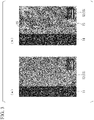
- Fig. 3 and Fig. 4 show the observation results of the bonding interface between either one of the circuit layer 12 or the metal layer 13 and the ceramic substrate 11 of the insulating circuit substrate 10 which is the present embodiment.
- the Al-Cu compound particles 15 are not present in the circuit layer 12 and the metal layer 13 and there is a microstructure in which Cu is solid-solubilized in the Al matrix.
- the number density of the Al-Cu compound particles 15 precipitated after carrying out 2000 thermal cycles, in which one cycle is holding at -65°C for 5 minutes and holding at 150°C for 5 minutes is preferably set in a range of 0.50 particles/ ⁇ m 2 or more and 8.50 particles/ ⁇ m 2 or less.
- the number density of the Al-Cu compound particles 15 is more preferably 0.60 particles/ ⁇ m 2 or more and even more preferably 0.75 particles/ ⁇ m 2 or more.
- the number density of the Al-Cu compound particles 15 is more preferably 8.30 particles/ ⁇ m 2 or less and even more preferably 8.10 particles/ ⁇ m 2 or less.
- the number density is calculated for Al-Cu compound particles having a particle diameter of 0.01 ⁇ m or more and 2 ⁇ m or less. In the calculation of the number density, in a case where the particle shape is not circular, the shortest part (short diameter) is determined as the particle diameter of that particle.
- the average of the equivalent circle diameters of the Al-Cu compound particles 15 precipitated after carrying out 2000 thermal cycles, in which one cycle is holding at -65°C for 5 minutes and holding at 150°C for 5 minutes is preferably set in a range of 30 nm or more and 130 nm or less.
- the average of the equivalent circle diameters of the Al-Cu compound particles 15 is more preferably 37 ⁇ m or more and even more preferably 45 ⁇ m or more.
- the average of the equivalent circle diameters of the Al-Cu compound particles 15 is more preferably 125 ⁇ m or less and even more preferably 120 ⁇ m or less.
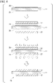
- a Cu layer 26 is formed on at least one of the bonding surface between the ceramic substrate 11 and the aluminum sheet 22 which is to be the circuit layer 12 and the bonding surface between the ceramic substrate 11 and the aluminum sheet 23 which is to be the metal layer 13.
- the Cu layers 26 are formed on both surfaces of the ceramic substrate 11 respectively.
- the method for forming the Cu layer 26 is not particularly limited and it is possible to use existing methods such as sputtering, vapor deposition, CVD, plating, paste, foil material, and the like as appropriate.
- the adhered amount of Cu in the Cu layer 26 is preferably in a range of 0.08 mg/cm 2 or more and 2.0 mg/cm 2 or less.
- the aluminum sheet 22, which becomes the circuit layer 12 is laminated on one surface of the ceramic substrate 11 via the Cu layer 26, and the aluminum sheet 23, which becomes the metal layer 13, is laminated on the other surface of the ceramic substrate 11 via the Cu layer 26.
- a laminate of the aluminum sheet 22, which becomes the circuit layer 12, the ceramic substrate 11, and the aluminum sheet 23, which becomes the metal layer 13, is charged into a vacuum heating furnace in a state of being pressed in the lamination direction using a pressing apparatus, the aluminum sheet 22 and the ceramic substrate 11 are bonded to form the circuit layer 12, and the aluminum sheet 23 and the ceramic substrate 11 are bonded to form the metal layer 13.
- the pressing load in the lamination direction is in a range of 0.098 MPa or more and 2.94 MPa or less.
- the bonding temperature is set in a range of 600°C or higher and 650°C or lower and the holding time at the bonding temperature is set to 180 minutes or less.
- the temperature increase rate from the eutectic temperature (548°C) of Al and Cu to the bonding temperature is set in a range of 5°C/min or more and 20°C/min or less.
- the insulating circuit substrate 10 which is the present embodiment is manufactured.
- the heat sink 31 is laminated on the other side of the metal layer 13 of the insulating circuit substrate 10 via a brazing material and the insulating circuit substrate 10 and the heat sink 31 are charged into a vacuum heating furnace in a state of being pressed in the lamination direction to bond the metal layer 13 and the heat sink 31.
- the semiconductor element 3 is laminated on one surface of the circuit layer 12 via the solder material (solder layer 2) and solder-bonded in the heating furnace.
- the power module 1 shown in Fig. 1 is manufactured.
- the insulating circuit substrate 10 which is the present embodiment configured as above, Cu is solid-solubilized on the bonding interface sides of the circuit layer 12 and the metal layer 13 with the ceramic substrate 11 and the ratio B/A between the Cu concentration A mass% at the bonding interface and the Cu concentration B mass% at a position of 100 ⁇ m in the thickness direction from the bonding interface to the circuit layer 12 and the metal layer 13 side is set to 0.30 or more and 0.85 or less.
- Cu is sufficiently diffused in the inside of the circuit layer 12 and the metal layer 13 formed of aluminum and a region where Cu is solid-solubilized in a supersaturated manner is formed in the vicinity of the bonding interface of the circuit layer 12 and metal layer 13.
- the circuit layer 12 and the metal layer 13 are strengthened and it is possible to suppress deformation of the circuit layer 12 and the metal layer 13 and the occurrence of cracks in the circuit layer 12 and the metal layer 13 after being subjected to thermal cycles.
- the amount of the hard Al-Cu eutectic phase is small and it is possible to suppress the occurrence of breaking in the ceramic substrate 11.
- the Cu concentration B at a position of 100 ⁇ m in the thickness direction from the bonding interface of the circuit layer 12 and the metal layer 13 with the ceramic substrate 11 is set in a range of 0.04 mass% or more and 0.96 mass% or less, Cu is sufficiently diffused toward the inside of the circuit layer 12 and the metal layer 13, and it is possible to further suppress the deformation of the circuit layer 12 and the metal layer 13 and the occurrence of cracks in the circuit layer 12 and the metal layer 13 after being subjected to thermal cycles.
- the Al-Cu compound particles 15 including Al and Cu are precipitated on the crystal grain boundaries and in the crystal grains of the circuit layer 12 and the metal layer 13 in a region up to 100 ⁇ m in the thickness direction from the bonding interface of the circuit layer 12 and the metal layer 13 with the ceramic substrate 11, the vicinity of the bonding interface of the circuit layer 12 and the metal layer 13 with the ceramic substrate 11 is strengthened by the Al-Cu compound particles 15. For this reason, it is possible to reliably suppress deformation of the circuit layer 12 and the metal layer 13 and the occurrence of cracks in the circuit layer 12 and the metal layer 13 after being subjected to thermal cycles.
- the deformation resistance in the vicinity of the bonding interface of the circuit layer 12 and the metal layer 13 increases and it is possible to further suppress the deformation of the circuit layer 12 and the metal layer 13. Furthermore, the vicinity of the bonding interface of the circuit layer 12 and the metal layer 13 does not become harder than necessary and it is possible to further suppress breaking in the ceramic substrate 11.
- the average equivalent circle diameter of the Al-Cu compound particles 15 is in a range of 30 nm or more and 130 nm or less, it is possible to sufficiently carry out precipitation strengthening of the portions in the vicinity of the bonding interface of the circuit layer 12 and the metal layer 13 and to further suppress the deformation of the circuit layer 12 and the metal layer 13.
- the ceramic substrate is described as being formed of silicon nitride, but is not limited thereto and may be formed of alumina or may be formed of aluminum nitride.
- the present embodiment is described as forming a power module with power semiconductor elements mounted on a circuit layer of an insulating circuit substrate, but is not limited thereto.
- an LED module may be formed by mounting an LED element on the insulating circuit substrate or a thermoelectric module may be formed by mounting a thermoelectric element on the circuit layer of the insulating circuit substrate.
- the insulating circuit substrate (the metal layer) and the heat sink are described as being bonded by brazing, but are not limited thereto and other bonding methods such as solid phase diffusion bonding and TLP may be applied.
- the heat sink is described as being formed of aluminum, but is not limited thereto and may be formed of copper or the like and may be provided with passages in which a cooling medium travels through an inner portion thereof.
- a buffer layer formed of, for example, 4N-aluminum may be provided between the heat sink and the insulating circuit substrate.
- a ceramic substrate (40 mm ⁇ 40 mm) shown in Table 1 was prepared and Cu layers were formed by a sputtering method on one surface and the other surface of the ceramic substrate. The adhered amount of Cu at this time is shown in Table 1.
- an aluminum sheet (37 mm ⁇ 37 mm ⁇ 0.4 mm thickness (t)) formed of 4N aluminum was laminated on one surface of the ceramic substrate via a Cu layer and an aluminum sheet (37 mm ⁇ 37 mm ⁇ 0.4 mm thickness (t)) formed of 4N aluminum was laminated on the other surface of the ceramic substrate via a Cu layer.
- the aluminum sheet and the ceramic substrate were bonded under the conditions shown in Table 1 to manufacture an insulating circuit substrate.
- the temperature increase rate shown in Table 1 is the temperature increase rate from the eutectic temperature (548°C) of Al and Cu to the bonding temperature.
- a heat sink (50 mm ⁇ 60 mm, 5 mm thick aluminum sheet (A6063)) was bonded to the metal layer of the obtained insulating circuit substrate via a buffer layer of 4N-aluminum (thickness 0.9 mm) to obtain an insulating circuit substrate with heat sink.
- the bonding of the metal layer to the buffer layer and the bonding of the buffer layer to the heat sink were performed by brazing using an Al-Si foil.
- the Cu concentration A at the bonding interface of the aluminum sheet, the Cu concentration B at the position 100 ⁇ m from the bonding interface to the inner portion of the aluminum sheet, the initial bonding rate, the presence or absence of Al-Cu compound particles after the thermal cycle test, the bonding rate after the thermal cycle test, and the presence or absence of breaking of the substrate after the thermal cycle test were evaluated.
- the insulating circuit substrate with heat sink was cut in cross-section along the lamination direction and quantitative analysis of Cu was performed in the cross-section in the center of the width direction of the substrate using an electron micro analyzer (JXA-8530F manufactured by JEOL Ltd.) under conditions where a magnification was 500 times and an acceleration voltage was 15 kV, at the bonding interface and at a position 100 ⁇ m from the bonding interface in the lamination direction.
- JXA-8530F manufactured by JEOL Ltd.
- the Cu concentrations at the bonding interface and at a position 100 ⁇ m from the bonding interface in the lamination direction in the observation region were determined at five points respectively and the average values thereof were calculated to obtain the Cu concentration A (mass%) at the bonding interface and the Cu concentration B (mass%) at a position of 100 ⁇ m from the bonding interface.
- the sum of the Al and Cu concentrations (mass%) at that time was set to 100 and the Cu concentration was calculated.
- the bonding rate between the aluminum sheet and the ceramic substrate was evaluated. Specifically, in the insulating circuit substrate with heat sink, the bonding rate of the interface between the aluminum sheet and the ceramic substrate was evaluated using an ultrasonic flaw detector (FineSAT200 manufactured by Hitachi Power Solutions Co., Ltd.) and calculated from the following formula.
- the insulating circuit substrate with heat sink was subjected to 2000 thermal cycles of -65°C ⁇ 5 minutes ⁇ 150°C ⁇ 5 minutes in a liquid bath (Fluorinert) using a TSB-51 cold thermal shock tester manufactured by ESPEC Corp.
- the insulating circuit substrate with heat sink after the thermal cycles described above was cut in the lamination direction, and then, in the cross-section in the center of the width direction of the substrate, a region (17 ⁇ m ⁇ 23 ⁇ m) including the bonding interface between the aluminum sheet and the ceramic substrate was observed using an electron scanning microscope (GeminiSEM 500 manufactured by Carl Zeiss) under conditions where a magnification was 5000 times and an acceleration voltage was 5.0 kV.
- the presence or absence of Al-Cu compound particles was evaluated by observing the region to 100 ⁇ m in the thickness direction from the bonding interface of the aluminum sheet.
- the insulating circuit substrate with heat sink after the thermal cycle test was evaluated using an ultrasonic flaw detector (FineSAT200 manufactured by Hitachi Power Solutions Co., Ltd.) as described above and the bonding rate was calculated.
- the presence or absence of breaking of the substrate was evaluated using an ultrasonic flaw detector (FineSAT200 manufactured by Hitachi Power Solutions Co., Ltd.). In a case where breaking was confirmed in any one of the circuit layer, metal layer, or ceramic substrate, the evaluation was "Yes" (breaking present).
- Comparative Examples 1 to 4 the ratio B/A between the Cu concentration A mass% at the bonding interface and the Cu concentration B mass% at a position of 100 ⁇ m in the thickness direction from the bonding interface to the aluminum sheet side was less than 0.30 or more than 0.85. In Comparative Examples 1 to 4, the bonding rate after the thermal cycle test was low and breaking was observed in the substrate after the thermal cycle test.
- the ratio B/A between the Cu concentration A mass% at the bonding interface and the Cu concentration B mass% at a position of 100 ⁇ m in the thickness direction from the bonding interface to the aluminum sheet side was 0.30 or more and 0.85 or less.
- the bonding rate was sufficiently high and no breaking was confirmed in the substrate even after the thermal cycle test.
- a ceramic substrate (40 mm ⁇ 40 mm) shown in Table 3 was prepared and Cu layers were formed by the sputtering method on one surface and the other surface of the ceramic substrate. The adhered amount of Cu at this time is shown in Table 3.
- an aluminum sheet (37 mm ⁇ 37 mm ⁇ 0.4 mm thickness (t)) formed of 4N aluminum was laminated on one surface of the ceramic substrate via a Cu layer and an aluminum sheet (37 mm ⁇ 37 mm ⁇ 0.4 mm thickness (t)) formed of 4N aluminum was laminated on the other surface of the ceramic substrate via a Cu layer.
- the aluminum sheet and the ceramic substrate were bonded under the conditions shown in Table 3 to manufacture an insulating circuit substrate.
- the Cu concentration A at the bonding interface of the aluminum sheet, the Cu concentration B at the position 100 ⁇ m from the bonding interface to the inner portion of the aluminum sheet, the initial bonding rate, the bonding rate after the thermal cycle test, and the presence or absence of breaking of the substrate after the thermal cycle test were evaluated using the same procedure as in Example 1.
- the area ratio of the Al-Cu eutectic phase at the bonding interface, the number density of the Al-Cu compound particles after the thermal cycle test, and the average equivalent circle diameter of the Al-Cu compound particles were evaluated as follows.
- a BSE image in the range of 1 mm from the end portion in the width direction toward the center was obtained by an electron scanning microscope (GeminiSEM 500 manufactured by Carl Zeiss) and this BSE image was binarized.
- the area of the Al-Cu eutectic phase and the area in a range up to 1 mm from the end portion of the bonding interface were determined and the area ratio of the Al-Cu eutectic phase at the bonding interface was calculated using the following formula.
- Area Ratio of Al ⁇ Cu eutectic phase area of Al ⁇ Cu eutectic phase / area from end portion to 1 mm toward center ⁇ 100 .
- the insulating circuit substrate after the thermal cycle test described above was cut in the lamination direction. Next, the presence or absence of Al-Cu compound particles was confirmed in the cross-section at the center of the substrate in the width direction by the method described above. In the region where Al-Cu compound particles were confirmed (in a range of 50 ⁇ m in the thickness direction from the bonding interface to the aluminum sheet side), an ASB image at a 1000-fold magnification was acquired using an electron scanning microscope (GeminiSEM 500 manufactured by Carl Zeiss) and the ASB image was binarized such that the Al-Cu compound particles were white.
- GaminiSEM 500 manufactured by Carl Zeiss
- the number of Al-Cu compound particles was measured and divided by the area of the measurement range to calculate the number density.
- the number density was calculated for Al-Cu compound particles having a particle diameter of 0.01 ⁇ m or more and 2 ⁇ m or less as a target.
- the shortest portion was determined as the particle diameter of that particle.
- the measurement was carried out after excluding this particle.
- the ASB image was binarized in the same manner as for the number density measurement method. Next, the area of each Al-Cu compound particle in the measurement region was determined, the equivalent circle diameter was calculated from this area, and the average value of the equivalent circle diameters was obtained. These average values are shown in Table 4. When determining the area, in cases where it was not possible to determine the area because a part of the particles was outside the measurement range, these pa rticles were excluded.
- the number density of the precipitated Al-Cu compound particles was in a range of 0.50 particles/ ⁇ m 2 or more and 8.50 particles/ ⁇ m 2 or less.
- the average equivalent circle diameter of the Al-Cu compound particles was in a range of 30 nm or more and 130 nm or less.
- the area ratio of the Al-Cu eutectic phase in a range of 1 mm from the end portion in the width direction toward the center of the bonding interface was 30.0% or less. Even after the thermal cycle test, the bonding rate was sufficiently high and no breaking was confirmed in the substrate.
- the area ratio of the Al-Cu eutectic phase was 32.0%.
- the number density of Al-Cu compound particles after the thermal cycle test was 8.70 particles/ ⁇ m 2 and the equivalent circle diameter of the Al-Cu compound particles was 27 nm.
- the number density of Al-Cu compound particles after the thermal cycle test was 0.47 particles/ ⁇ m 2 and the equivalent circle diameter of the Al-Cu compound particles was 133 nm.
- the area ratio of the Al-Cu eutectic phase was 30.0% or less
- the number density of the Al-Cu compound particles after the thermal cycle test was in a range of 0.50 particles/ ⁇ m 2 or more and 8.50 particles/ ⁇ m 2 or less
- the equivalent circle diameter of the Al-Cu compound particles was 30 nm or more and 130 nm or less. It was confirmed that the bonding rate was even better in Inventive Examples 11, 13, 15, 17, and 18 than that in Inventive Examples 12, 14, and 16.
- the insulating circuit substrate of the present embodiment to power modules, LED modules, and thermoelectric modules.
Landscapes
- Engineering & Computer Science (AREA)
- Chemical & Material Sciences (AREA)
- Microelectronics & Electronic Packaging (AREA)
- Ceramic Engineering (AREA)
- Manufacturing & Machinery (AREA)
- Materials Engineering (AREA)
- Structural Engineering (AREA)
- Organic Chemistry (AREA)
- Cooling Or The Like Of Semiconductors Or Solid State Devices (AREA)
- Physics & Mathematics (AREA)
- Geometry (AREA)
Applications Claiming Priority (3)
| Application Number | Priority Date | Filing Date | Title |
|---|---|---|---|
| JP2020047956 | 2020-03-18 | ||
| JP2021040435A JP6973674B2 (ja) | 2020-03-18 | 2021-03-12 | 絶縁回路基板 |
| PCT/JP2021/010548 WO2021187464A1 (fr) | 2020-03-18 | 2021-03-16 | Carte de circuit isolée |
Publications (2)
| Publication Number | Publication Date |
|---|---|
| EP4123697A1 true EP4123697A1 (fr) | 2023-01-25 |
| EP4123697A4 EP4123697A4 (fr) | 2024-04-24 |
Family
ID=77771126
Family Applications (1)
| Application Number | Title | Priority Date | Filing Date |
|---|---|---|---|
| EP21772541.5A Pending EP4123697A4 (fr) | 2020-03-18 | 2021-03-16 | Carte de circuit isolée |
Country Status (5)
| Country | Link |
|---|---|
| US (1) | US12089342B2 (fr) |
| EP (1) | EP4123697A4 (fr) |
| KR (1) | KR20220154663A (fr) |
| TW (1) | TW202142060A (fr) |
| WO (1) | WO2021187464A1 (fr) |
Family Cites Families (11)
| Publication number | Priority date | Publication date | Assignee | Title |
|---|---|---|---|---|
| JP3171234B2 (ja) | 1997-03-26 | 2001-05-28 | 三菱マテリアル株式会社 | ヒートシンク付セラミック回路基板 |
| CN102047413B (zh) | 2008-06-06 | 2015-04-15 | 三菱综合材料株式会社 | 功率模块用基板、功率模块以及功率模块用基板的制造方法 |
| JP5359953B2 (ja) | 2009-03-26 | 2013-12-04 | 三菱マテリアル株式会社 | パワーモジュール用基板、パワーモジュール及びパワーモジュール用基板の製造方法 |
| CN102498564B (zh) * | 2009-09-09 | 2015-08-26 | 三菱综合材料株式会社 | 带散热器的功率模块用基板的制造方法、带散热器的功率模块用基板及功率模块 |
| JP5664038B2 (ja) | 2010-09-07 | 2015-02-04 | 三菱マテリアル株式会社 | パワーモジュール用基板、パワーモジュール用基板の製造方法及びパワーモジュール |
| US9947688B2 (en) | 2011-06-22 | 2018-04-17 | Psemi Corporation | Integrated circuits with components on both sides of a selected substrate and methods of fabrication |
| CN103733329B (zh) * | 2011-08-12 | 2016-10-26 | 三菱综合材料株式会社 | 功率模块用基板、自带散热器的功率模块用基板、功率模块以及功率模块用基板的制造方法 |
| JP2013229579A (ja) * | 2012-03-30 | 2013-11-07 | Mitsubishi Materials Corp | パワーモジュール用基板、ヒートシンク付パワーモジュール用基板及びパワーモジュール |
| KR102300413B1 (ko) | 2014-03-20 | 2021-09-08 | 미쓰비시 마테리알 가부시키가이샤 | 접합체, 파워 모듈용 기판, 파워 모듈 및 접합체의 제조 방법 |
| WO2019146464A1 (fr) * | 2018-01-25 | 2019-08-01 | 三菱マテリアル株式会社 | Corps lié cuivre/céramique, carte de circuit imprimé isolante, procédé de production de corps lié cuivre/céramique, et procédé de production de carte de circuit imprimé isolante |
| JP2021040435A (ja) | 2019-09-04 | 2021-03-11 | 本田技研工業株式会社 | 充電制御システム、自律走行作業機、及び充電ステーション |
-
2021
- 2021-03-16 WO PCT/JP2021/010548 patent/WO2021187464A1/fr not_active Ceased
- 2021-03-16 US US17/793,721 patent/US12089342B2/en active Active
- 2021-03-16 KR KR1020227025445A patent/KR20220154663A/ko not_active Withdrawn
- 2021-03-16 EP EP21772541.5A patent/EP4123697A4/fr active Pending
- 2021-03-17 TW TW110109526A patent/TW202142060A/zh unknown
Also Published As
| Publication number | Publication date |
|---|---|
| KR20220154663A (ko) | 2022-11-22 |
| US12089342B2 (en) | 2024-09-10 |
| US20230091454A1 (en) | 2023-03-23 |
| CN115039217A (zh) | 2022-09-09 |
| TW202142060A (zh) | 2021-11-01 |
| WO2021187464A1 (fr) | 2021-09-23 |
| EP4123697A4 (fr) | 2024-04-24 |
Similar Documents
| Publication | Publication Date | Title |
|---|---|---|
| EP3590909B1 (fr) | Carte de circuit imprimé isolée à corps assemblé en cuivre/céramique, procédé de production de corps assemblé en cuivre/céramique, et procédé de production de carte de circuit imprimé isolée | |
| CN101861647B (zh) | 电源模块用基板的制造方法、电源模块用基板、和电源模块 | |
| CN109417056B (zh) | 铜-陶瓷接合体及绝缘电路基板 | |
| EP2911192B1 (fr) | Substrat destiné à un bloc de puissance doté d'un puits de chaleur, bloc de puissance doté d'un puits de chaleur, et procédé de production d'un substrat destiné à un bloc de puissance doté d'un puits de chaleur | |
| EP2833399B1 (fr) | Substrat de module de puissance, substrat de module de puissance muni de dissipateur thermique, et module de puissance | |
| EP3744705B1 (fr) | Corps lié cuivre/céramique, carte de circuit imprimé isolante, procédé de production de corps lié cuivre/céramique, et procédé de production de carte de circuit imprimé isolante | |
| TWI695778B (zh) | 接合體、附散熱器之電力模組用基板、散熱器、接合體之製造方法、附散熱器之電力模組用基板之製造方法、及散熱器之製造方法 | |
| EP2833400B1 (fr) | Substrat de module de puissance muni de dissipateur thermique, et procédé de fabrication de substrat de module de puissance muni de dissipateur thermique | |
| TWI581342B (zh) | 功率模組 | |
| EP3041043A1 (fr) | Ensemble et substrat de module de puissance | |
| EP2282334B1 (fr) | Procédé de fabrication de substrat pour module de puissance | |
| EP3196930B1 (fr) | Corps soudé, substrat de module de puissance avec dissipateur thermique, utilisation du corps soudé comme dissipateur thermique, procédé de fabrication du corps soudé | |
| TWI700263B (zh) | 陶瓷-鋁接合體、電力模組用基板、及電力模組 | |
| KR20180077204A (ko) | 세라믹스/알루미늄 접합체, 절연 회로 기판, 파워 모듈, led 모듈, 열전 모듈 | |
| JP7512863B2 (ja) | 銅/セラミックス接合体、絶縁回路基板、及び、銅/セラミックス接合体の製造方法、絶縁回路基板の製造方法 | |
| US12089342B2 (en) | Insulated circuit board | |
| CN114787106B (zh) | 铜-陶瓷接合体、绝缘电路基板及铜-陶瓷接合体的制造方法、绝缘电路基板的制造方法 | |
| EP3703116B1 (fr) | Corps lié, carte de circuit isolée avec dissipateur thermique, et dissipateur thermique | |
| WO2017090422A1 (fr) | Corps assemblé céramique/aluminium, carte de circuit imprimé isolé, module de puissance, module del et module thermoélectrique | |
| CN115039217B (en) | Insulated circuit board | |
| JP6973674B2 (ja) | 絶縁回路基板 | |
| JP2023141007A (ja) | 絶縁回路基板 |
Legal Events
| Date | Code | Title | Description |
|---|---|---|---|
| STAA | Information on the status of an ep patent application or granted ep patent |
Free format text: STATUS: THE INTERNATIONAL PUBLICATION HAS BEEN MADE |
|
| PUAI | Public reference made under article 153(3) epc to a published international application that has entered the european phase |
Free format text: ORIGINAL CODE: 0009012 |
|
| STAA | Information on the status of an ep patent application or granted ep patent |
Free format text: STATUS: REQUEST FOR EXAMINATION WAS MADE |
|
| 17P | Request for examination filed |
Effective date: 20220721 |
|
| AK | Designated contracting states |
Kind code of ref document: A1 Designated state(s): AL AT BE BG CH CY CZ DE DK EE ES FI FR GB GR HR HU IE IS IT LI LT LU LV MC MK MT NL NO PL PT RO RS SE SI SK SM TR |
|
| DAV | Request for validation of the european patent (deleted) | ||
| DAX | Request for extension of the european patent (deleted) | ||
| REG | Reference to a national code |
Ref country code: DE Ref legal event code: R079 Free format text: PREVIOUS MAIN CLASS: H01L0023130000 Ipc: C04B0037020000 |
|
| A4 | Supplementary search report drawn up and despatched |
Effective date: 20240322 |
|
| RIC1 | Information provided on ipc code assigned before grant |
Ipc: H01L 23/373 20060101ALI20240318BHEP Ipc: H01L 23/36 20060101ALI20240318BHEP Ipc: H01L 23/12 20060101ALI20240318BHEP Ipc: H01L 23/13 20060101ALI20240318BHEP Ipc: C04B 37/02 20060101AFI20240318BHEP |