EP4130548B1 - Rückbeleuchtungseinheit und bildanzeigevorrichtung - Google Patents
Rückbeleuchtungseinheit und bildanzeigevorrichtung Download PDFInfo
- Publication number
- EP4130548B1 EP4130548B1 EP21775781.4A EP21775781A EP4130548B1 EP 4130548 B1 EP4130548 B1 EP 4130548B1 EP 21775781 A EP21775781 A EP 21775781A EP 4130548 B1 EP4130548 B1 EP 4130548B1
- Authority
- EP
- European Patent Office
- Prior art keywords
- sensitive adhesive
- layer
- light
- refractive index
- guide plate
- Prior art date
- Legal status (The legal status is an assumption and is not a legal conclusion. Google has not performed a legal analysis and makes no representation as to the accuracy of the status listed.)
- Active
Links
Images
Classifications
-
- G—PHYSICS
- G02—OPTICS
- G02F—OPTICAL DEVICES OR ARRANGEMENTS FOR THE CONTROL OF LIGHT BY MODIFICATION OF THE OPTICAL PROPERTIES OF THE MEDIA OF THE ELEMENTS INVOLVED THEREIN; NON-LINEAR OPTICS; FREQUENCY-CHANGING OF LIGHT; OPTICAL LOGIC ELEMENTS; OPTICAL ANALOGUE/DIGITAL CONVERTERS
- G02F1/00—Devices or arrangements for the control of the intensity, colour, phase, polarisation or direction of light arriving from an independent light source, e.g. switching, gating or modulating; Non-linear optics
- G02F1/01—Devices or arrangements for the control of the intensity, colour, phase, polarisation or direction of light arriving from an independent light source, e.g. switching, gating or modulating; Non-linear optics for the control of the intensity, phase, polarisation or colour
- G02F1/13—Devices or arrangements for the control of the intensity, colour, phase, polarisation or direction of light arriving from an independent light source, e.g. switching, gating or modulating; Non-linear optics for the control of the intensity, phase, polarisation or colour based on liquid crystals, e.g. single liquid crystal display cells
- G02F1/133—Constructional arrangements; Operation of liquid crystal cells; Circuit arrangements
- G02F1/1333—Constructional arrangements; Manufacturing methods
- G02F1/1335—Structural association of cells with optical devices, e.g. polarisers or reflectors
- G02F1/1336—Illuminating devices
- G02F1/133615—Edge-illuminating devices, i.e. illuminating from the side
-
- F—MECHANICAL ENGINEERING; LIGHTING; HEATING; WEAPONS; BLASTING
- F21—LIGHTING
- F21S—NON-PORTABLE LIGHTING DEVICES; SYSTEMS THEREOF; VEHICLE LIGHTING DEVICES SPECIALLY ADAPTED FOR VEHICLE EXTERIORS
- F21S2/00—Systems of lighting devices, not provided for in main groups F21S4/00 - F21S10/00 or F21S19/00, e.g. of modular construction
-
- G—PHYSICS
- G02—OPTICS
- G02B—OPTICAL ELEMENTS, SYSTEMS OR APPARATUS
- G02B6/00—Light guides; Structural details of arrangements comprising light guides and other optical elements, e.g. couplings
- G02B6/0001—Light guides; Structural details of arrangements comprising light guides and other optical elements, e.g. couplings specially adapted for lighting devices or systems
- G02B6/0011—Light guides; Structural details of arrangements comprising light guides and other optical elements, e.g. couplings specially adapted for lighting devices or systems the light guides being planar or of plate-like form
- G02B6/0081—Mechanical or electrical aspects of the light guide and light source in the lighting device peculiar to the adaptation to planar light guides, e.g. concerning packaging
- G02B6/0086—Positioning aspects
- G02B6/0088—Positioning aspects of the light guide or other optical sheets in the package
-
- G—PHYSICS
- G02—OPTICS
- G02B—OPTICAL ELEMENTS, SYSTEMS OR APPARATUS
- G02B6/00—Light guides; Structural details of arrangements comprising light guides and other optical elements, e.g. couplings
- G02B6/0001—Light guides; Structural details of arrangements comprising light guides and other optical elements, e.g. couplings specially adapted for lighting devices or systems
- G02B6/0011—Light guides; Structural details of arrangements comprising light guides and other optical elements, e.g. couplings specially adapted for lighting devices or systems the light guides being planar or of plate-like form
- G02B6/0033—Means for improving the coupling-out of light from the light guide
- G02B6/005—Means for improving the coupling-out of light from the light guide provided by one optical element, or plurality thereof, placed on the light output side of the light guide
- G02B6/0055—Reflecting element, sheet or layer
-
- G—PHYSICS
- G02—OPTICS
- G02F—OPTICAL DEVICES OR ARRANGEMENTS FOR THE CONTROL OF LIGHT BY MODIFICATION OF THE OPTICAL PROPERTIES OF THE MEDIA OF THE ELEMENTS INVOLVED THEREIN; NON-LINEAR OPTICS; FREQUENCY-CHANGING OF LIGHT; OPTICAL LOGIC ELEMENTS; OPTICAL ANALOGUE/DIGITAL CONVERTERS
- G02F1/00—Devices or arrangements for the control of the intensity, colour, phase, polarisation or direction of light arriving from an independent light source, e.g. switching, gating or modulating; Non-linear optics
- G02F1/01—Devices or arrangements for the control of the intensity, colour, phase, polarisation or direction of light arriving from an independent light source, e.g. switching, gating or modulating; Non-linear optics for the control of the intensity, phase, polarisation or colour
- G02F1/13—Devices or arrangements for the control of the intensity, colour, phase, polarisation or direction of light arriving from an independent light source, e.g. switching, gating or modulating; Non-linear optics for the control of the intensity, phase, polarisation or colour based on liquid crystals, e.g. single liquid crystal display cells
- G02F1/133—Constructional arrangements; Operation of liquid crystal cells; Circuit arrangements
- G02F1/1333—Constructional arrangements; Manufacturing methods
- G02F1/1335—Structural association of cells with optical devices, e.g. polarisers or reflectors
- G02F1/1336—Illuminating devices
-
- F—MECHANICAL ENGINEERING; LIGHTING; HEATING; WEAPONS; BLASTING
- F21—LIGHTING
- F21V—FUNCTIONAL FEATURES OR DETAILS OF LIGHTING DEVICES OR SYSTEMS THEREOF; STRUCTURAL COMBINATIONS OF LIGHTING DEVICES WITH OTHER ARTICLES, NOT OTHERWISE PROVIDED FOR
- F21V2200/00—Use of light guides, e.g. fibre optic devices, in lighting devices or systems
- F21V2200/20—Use of light guides, e.g. fibre optic devices, in lighting devices or systems of light guides of a generally planar shape
-
- F—MECHANICAL ENGINEERING; LIGHTING; HEATING; WEAPONS; BLASTING
- F21—LIGHTING
- F21Y—INDEXING SCHEME ASSOCIATED WITH SUBCLASSES F21K, F21L, F21S and F21V, RELATING TO THE FORM OR THE KIND OF THE LIGHT SOURCES OR OF THE COLOUR OF THE LIGHT EMITTED
- F21Y2103/00—Elongate light sources, e.g. fluorescent tubes
-
- F—MECHANICAL ENGINEERING; LIGHTING; HEATING; WEAPONS; BLASTING
- F21—LIGHTING
- F21Y—INDEXING SCHEME ASSOCIATED WITH SUBCLASSES F21K, F21L, F21S and F21V, RELATING TO THE FORM OR THE KIND OF THE LIGHT SOURCES OR OF THE COLOUR OF THE LIGHT EMITTED
- F21Y2115/00—Light-generating elements of semiconductor light sources
- F21Y2115/10—Light-emitting diodes [LED]
-
- G—PHYSICS
- G02—OPTICS
- G02F—OPTICAL DEVICES OR ARRANGEMENTS FOR THE CONTROL OF LIGHT BY MODIFICATION OF THE OPTICAL PROPERTIES OF THE MEDIA OF THE ELEMENTS INVOLVED THEREIN; NON-LINEAR OPTICS; FREQUENCY-CHANGING OF LIGHT; OPTICAL LOGIC ELEMENTS; OPTICAL ANALOGUE/DIGITAL CONVERTERS
- G02F1/00—Devices or arrangements for the control of the intensity, colour, phase, polarisation or direction of light arriving from an independent light source, e.g. switching, gating or modulating; Non-linear optics
- G02F1/01—Devices or arrangements for the control of the intensity, colour, phase, polarisation or direction of light arriving from an independent light source, e.g. switching, gating or modulating; Non-linear optics for the control of the intensity, phase, polarisation or colour
- G02F1/13—Devices or arrangements for the control of the intensity, colour, phase, polarisation or direction of light arriving from an independent light source, e.g. switching, gating or modulating; Non-linear optics for the control of the intensity, phase, polarisation or colour based on liquid crystals, e.g. single liquid crystal display cells
- G02F1/133—Constructional arrangements; Operation of liquid crystal cells; Circuit arrangements
- G02F1/1333—Constructional arrangements; Manufacturing methods
- G02F1/1335—Structural association of cells with optical devices, e.g. polarisers or reflectors
- G02F1/1336—Illuminating devices
- G02F1/133602—Direct backlight
- G02F1/133608—Direct backlight including particular frames or supporting means
-
- G—PHYSICS
- G02—OPTICS
- G02F—OPTICAL DEVICES OR ARRANGEMENTS FOR THE CONTROL OF LIGHT BY MODIFICATION OF THE OPTICAL PROPERTIES OF THE MEDIA OF THE ELEMENTS INVOLVED THEREIN; NON-LINEAR OPTICS; FREQUENCY-CHANGING OF LIGHT; OPTICAL LOGIC ELEMENTS; OPTICAL ANALOGUE/DIGITAL CONVERTERS
- G02F2202/00—Materials and properties
- G02F2202/28—Adhesive materials or arrangements
Definitions
- the present invention relates to a backlight unit.
- a liquid crystal display apparatus has been used in a wide variety of applications including a portable terminal, a personal computer, a car navigation system, and a television.
- a planar backlight which is arranged on the back surface side of its liquid crystal panel and emits light in a planar fashion, has been frequently used.
- An edge light (side light) system in which a light source is arranged to face the end surface of a light guide plate and light that has entered from the end surface is emitted from the emitting surface of the light guide plate is often adopted for the planar backlight.
- the back surface side of the light guide plate is typically bonded to a flexible printed circuit board (FPC) via a white diffusing tape.
- FPC flexible printed circuit board
- the front surface side of the light guide plate is typically supported and fixed by the front portion of a casing in which the light guide plate is stored, and as a result, the entirety of the light guide plate is fixed in the casing.
- Such configuration has involved a problem in that a brightness loss occurs.
- a technology including bonding the light guide plate and the FPC to each other via a double-sided pressure-sensitive adhesive film including a low-refractive index layer having a refractive index of 1.25 or less Patent Literature 1).
- a further improvement in performance e.g., brightness loss suppressibility (lightness) or light leakage suppressibility
- the present invention has been made to solve the above-mentioned conventional problem, and a primary object of the present invention is to provide a backlight unit, which is bright and is suppressed from causing light leakage in an oblique direction.
- a backlight unit includes: a light source; a light guide plate having an end surface that is arranged to face the light source, and that light from the light source enters, and an emitting surface from which the entered light is emitted; a casing having a front portion and a back portion, the casing being configured to store the light source and the light guide plate; and an optical pressure-sensitive adhesive film arranged between the front portion of the casing on a light source side and the light guide plate, the optical pressure-sensitive adhesive film being bonded to the light guide plate.
- the optical pressure-sensitive adhesive film includes a light-absorbing layer, a substrate, a low-refractive index layer, and a pressure-sensitive adhesive layer in the stated order from a front portion side of the casing.
- the backlight unit further includes a reflective plate arranged in the casing on a back surface side of the light guide plate.
- the reflective plate is arranged via an air layer between the reflective plate and the light guide plate.
- the reflective plate and the light guide plate are bonded to each other via a double-sided pressure-sensitive adhesive film including a low-refractive index layer.
- the light source is a LED light source.
- an image display apparatus includes: the backlight unit as described above; and an image display panel arranged on an emitting surface side of the light guide plate.
- the optical pressure-sensitive adhesive film including the light-absorbing layer and the low-refractive index layer in a predetermined positional relationship is arranged between the front portion of the casing on the light source side and the light guide plate.
- the backlight unit which is bright and is suppressed from causing light leakage in an oblique direction, can be achieved.
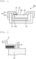
- FIG. 1 is a schematic sectional view of a backlight unit according to one embodiment of the present invention
- FIG. 2 is an enlarged schematic sectional view of the portion II of the backlight unit of FIG. 1
- a backlight unit 100 of the illustrated example includes a light source 10 , a light guide plate 20, a casing 30, and an optical pressure-sensitive adhesive film 40.
- the casing 30 has a front portion 31 and a back portion 32, and stores the light source 10 and the light guide plate 20.
- the back portion 32 has a box shape whose upper portion (front surface side) is opened, and in a pair of end portions of the back portion 32 opposing each other, the front portion 31 protrudes inward from the back portion in the illustrated example.
- the front portion 31 may not protrude inward in the end portions.
- the front portion 31 and the back portion 32 are typically fixed to and integrated with each other.
- the light guide plate 20 can be typically fit into the casing 30.
- Any appropriate optical member (not shown) may be typically mounted (bridged) on the step portions (portions protruding inward) of the front portion. No step portions may be arranged in the front portion.
- Examples of the optical member include a diffusing sheet and a prism sheet.
- the diffusing sheet and/or the prism sheet may be mounted in plurality.
- the casing 30 of the illustrated example may be a part of the back portion of the casing for storing the entirety of an image display apparatus.
- the light source 10 is arranged on one end portion side of the light guide plate 20 to face an end surface 20a of the light guide plate. Accordingly, the backlight unit is typically an edge light system.
- the light source 10 is typically surrounded by a reflector (not shown). Any appropriate configuration may be adopted as the light source. Specific examples thereof include a light emitting diode (LED), a cold cathode fluorescent lamp (CCFL), an external electrode fluorescent lamp (EEFL), and a hot cathode fluorescent lamp (HCFL).
- a LED light source may be used.
- the LED light source may be typically formed by arranging LEDs (point light sources) in a line.
- the light guide plate 20 has the end surface 20a that light from the light source enters and an emitting surface 20b from which the entered light is emitted.
- the end surface 20a of the light guide plate 20 is arranged to face the light source 10 . More specifically, the light guide plate 20 guides the light that has entered the end surface 20a from the light source 10 toward an end portion opposite to the end surface 20a while subjecting the light to a reflective action or the like therein, and in the light guide process, the plate gradually emits the light from the emitting surface 20b .
- An emission pattern is typically arranged on the emitting surface 20b .
- the emission pattern is, for example, an uneven shape.
- a light extraction pattern is typically arranged on the surface of the light guide plate opposite to the emitting surface.
- the light extraction pattern is, for example, a white dot. Any appropriate configuration may be adopted as the light guide plate.
- the back surface side of the light guide plate 20 is bonded to a flexible printed circuit board for a light source via any appropriate means (e.g., a pressure-sensitive adhesive tape).
- the optical pressure-sensitive adhesive film 40 is arranged between the front portion 31 of the casing 30 on the light source 10 side and the light guide plate 20.
- the optical pressure-sensitive adhesive film 40 includes a light-absorbing layer 41, a substrate 42, a low-refractive index layer 43, and a pressure-sensitive adhesive layer 44 in the stated order from the front portion 31 side of the casing 30. Part of the optical pressure-sensitive adhesive film 40 is bonded to the light guide plate 20 via the pressure-sensitive adhesive layer 44.
- the optical pressure-sensitive adhesive film protrudes from the light guide plate toward the light source in the illustrated example, the end surface of the optical pressure-sensitive adhesive film and the end surface of the light guide plate may be flush with each other.
- the reflective plate include: a resin sheet having a high reflectance (e.g., an acrylic plate); a metal thin plate or metal foil made of aluminum, stainless steel, or the like; a deposited sheet obtained by depositing aluminum, silver, or the like from the vapor onto a substrate such as a resin film made of polyester or the like; a laminate of a substrate such as a resin film made of polyester or the like and metal foil made of aluminum or the like; and a resin film having formed therein voids.
- the arrangement of the reflective plate 50 can improve light utilization efficiency in the backlight unit.
- optical pressure-sensitive adhesive film 40 and the double-sided pressure-sensitive adhesive film are described in detail below.
- the optical pressure-sensitive adhesive film 40 includes the light-absorbing layer 41, the substrate 42, the low-refractive index layer 43, and the pressure-sensitive adhesive layer 44 in the stated order from the front portion 31 side of the casing 30.
- the light-absorbing layer 41 may be a design layer having arranged thereon a predetermined design, or may be a solid colored layer.
- the light-absorbing layer is preferably a solid colored layer, more preferably a black colored layer.
- the total light transmittance of the light-absorbing layer in a thickness of from 3 ⁇ m to 5 ⁇ m is preferably 0.01% or less, more preferably 0.008% or less.
- the total light transmittance of the light-absorbing layer is preferably as small as possible, and its lower limit may be, for example, 0.001%. When the total light transmittance of the light-absorbing layer falls within such ranges, the layer can achieve more excellent light-absorbing and shielding functions.
- the thickness of the light-absorbing layer is preferably from 0.1 ⁇ m to 300 ⁇ m. When the thickness falls within such range, appropriate selection of a material for forming the layer facilitates the achievement of a desired total light transmittance (consequently, desired light-absorbing and shielding functions).
- the light-absorbing layer may be formed by any appropriate printing method using any appropriate ink or paint.
- Specific examples of the printing method include ink jet printing, gravure printing, offset printing, silkscreen printing, and transfer printing from a transfer sheet.
- the ink or paint to be used typically contains a binder, a colorant, a solvent, and any appropriate additive that may be used as required.
- the binder include chlorinated polyolefins (e.g., chlorinated polyethylene and chlorinated polypropylene), a polyester-based resin, a urethane-based resin, an acrylic resin, a vinyl acetate resin, a vinyl chloride-vinyl acetate copolymer, and a cellulose-based resin.
- the binder resins may be used alone or in combination thereof.
- the binder resin may be a thermally polymerizable resin or a photopolymerizable resin.
- the binder resin is an acrylic resin, preferably an acrylic resin containing a polyfunctional monomer (e.g., pentaerythritol triacrylate) as a copolymerization component.
- a polyfunctional monomer e.g., pentaerythritol triacrylate
- a colored layer having an appropriate modulus of elasticity can be formed.
- any appropriate colorant may be used as the colorant depending on purposes.
- the colorant include: inorganic pigments, such as titanium white, zinc white, carbon black, iron black, iron oxide red, chrome vermilion, ultramarine, cobalt blue, chrome yellow, and titanium yellow; organic pigments or dyes, such as phthalocyanine blue, indanthrene blue, isoindolinone yellow, benzidine yellow, quinacridone red, polyazo red, perylene red, and aniline black; metal pigments formed of scale-like foil pieces of aluminum, brass, and the like; and pearlescent pigments (pearl pigments) formed of scale-like foil pieces of titanium dioxide-coated mica, basic lead carbonate, and the like.
- inorganic pigments such as titanium white, zinc white, carbon black, iron black, iron oxide red, chrome vermilion, ultramarine, cobalt blue, chrome yellow, and titanium yellow
- organic pigments or dyes such as phthalocyanine blue, indanthrene blue, isoindolinone yellow
- the black colored layer When the black colored layer is formed, carbon black, iron black, or aniline black is suitably used.
- the colorants are preferably used in combination thereof. This is because a colored layer having no hue (that is, being jet black) by absorbing visible light in a wide range and uniformly can be formed.
- an azo compound and/or a quinone compound may be used.
- the colorant contains the carbon black as a main component and another colorant (e.g., an azo compound and/or a quinone compound). According to such configuration, a colored layer having no hue and being excellent in temporal stability can be formed.
- the colorant When the black colored layer is formed, the colorant may be used at a ratio of preferably from 1 part by weight to 200 parts by weight with respect to 100 parts by weight of the binder resin. In this case, the content of the carbon black in the colorant is preferably from 1% to 100%. When the colorant (in particular, the carbon black) is used at such ratio, a colored layer having an extremely low total light transmittance and being excellent in temporal stability can be formed.
- the substrate 42 may be typically formed of a film or plate-shaped product of a resin (preferably a transparent resin) .
- a resin preferably a transparent resin
- Typical examples of such resin include a thermoplastic resin and a reactive resin (e.g., an ionizing radiation-curable resin).
- the thermoplastic resin include: a (meth)acrylic resin, such as polymethyl methacrylate (PMMA) or polyacrylonitrile; a polycarbonate (PC) resin; a polyester resin such as PET; a cellulose-based resin such as triacetyl cellulose (TAC) ; a cyclic polyolefin-based resin; and a styrene-based resin.
- Specific examples of the ionizing radiation-curable resin include an epoxy acrylate-based resin and a urethane acrylate-based resin. Those resins may be used alone or in combination thereof.
- the thickness of the substrate is, for example, from 10 ⁇ m to 100 ⁇ m, preferably from 10 ⁇ m to 50 ⁇ m.
- the refractive index of the substrate is preferably 1.47 or more, more preferably from 1.47 to 1.60, still more preferably from 1.47 to 1.55. When the refractive index falls within such ranges, light extracted from the light guide plate can be introduced into an image display cell without being adversely affected.
- the low-refractive index layer typically has pores therein.
- the porosity of the low-refractive index layer is, for example, 40% or more, typically 50% or more, preferably 70% or more, more preferably 80% or more. Meanwhile, the porosity is, for example, 90% or less, preferably 85% or less.
- the refractive index of the low-refractive index layer can be set within an appropriate range.
- the porosity is a value calculated from the value of the refractive index measured with an ellipsometer by using Lorentz-Lorenz's formula.
- the refractive index of the low-refractive index layer is preferably 1.30 or less, more preferably 1.20 or less, still more preferably 1.15 or less.
- the lower limit of the refractive index may be, for example, 1.01. When the refractive index falls within such ranges, extremely excellent light utilization efficiency can be achieved in the backlight unit.
- the refractive index refers to a refractive index measured at a wavelength of 550 nm unless otherwise stated.
- the refractive index is a value measured by a method described in the section " (1) Refractive Index of Low-refractive Index Layer" in Examples below.
- the low-refractive index layer may be preferably formed through, for example, application or printing. Materials described in, for example, WO 2004/113966 A1 , JP 2013-254183 A , and JP 2012-189802 A may each be adopted as a material for forming the low-refractive index layer.
- silica-based compounds include: silica-based compounds; hydrolyzable silanes, and partial hydrolysates and dehydration condensates thereof; organic polymers; silanol group-containing silicon compounds; active silica obtained by bringing a silicate into contact with an acid or an ion-exchange resin; polymerizable monomers (e.g., a (meth) acrylic monomer and a styrene-based monomer); curable resins (e.g., a (meth)acrylic resin, a fluorine-containing resin, and a urethane resin); and combinations thereof.
- the low-refractive index layer may be formed by, for example, applying or printing a solution or a dispersion liquid of such material.
- the size of each of the pores (holes) in the low-refractive index layer refers to a major axis diameter out of the major axis diameter and minor axis diameter of the pore (hole) .
- the sizes of the pores (holes) are, for example, from 2 nm to 500 nm.
- the sizes of the pores (holes) are, for example, 2 nm or more, preferably 5 nm or more, more preferably 10 nm or more, still more preferably 20 nm or more.
- the sizes of the pores (holes) are, for example, 500 nm or less, preferably 200 nm or less, more preferably 100 nm or less.
- the range of the sizes of the pores (holes) is, for example, from 2 nm to 500 nm, preferably from 5 nm to 500 nm, more preferably from 10 nm to 200 nm, still more preferably from 20 nm to 100 nm.
- the sizes of the pores (holes) may be adjusted to desired sizes in accordance with, for example, a purpose and an application.
- the sizes of the pores (holes) may be quantified by a BET test method.
- the sizes of the pores (holes) may be quantified by a BET test method. Specifically, 0.1 g of the sample (formed pore layer) is loaded into the capillary of a specific surface area-measuring apparatus (manufactured by Micromeritics Instrument Corporation, ASAP 2020), and is then dried under reduced pressure at room temperature for 24 hours so that a gas in its pore structure may be removed. Then, an adsorption isotherm is drawn by causing the sample to adsorb a nitrogen gas, and its pore size distribution is determined. Thus, the pore sizes may be evaluated.
- the haze of the low-refractive index layer is, for example, less than 5%, preferably less than 3%. Meanwhile, the haze is, for example, 0.1% or more, preferably 0.2% or more. The range of the haze is, for example, 0.1% or more and less than 5%, preferably 0.2% or more and less than 3%.
- the haze is an indicator of the transparency of the low-refractive index layer, and may be measured by, for example, such a method as described below.
- the pore layer (low-refractive index layer) is cut into a size measuring 50 mm by 50 mm, and is set in a haze meter (manufactured by Murakami Color Research Laboratory Co., Ltd.: HM-150), followed by the measurement of its haze.
- the low-refractive index layer having the pores therein is, for example, a low-refractive index layer having a porous layer and/or an air layer in at least part thereof.
- the porous layer typically contains aerogel and/or particles (e.g., hollow fine particles and/or porous particles).
- the low-refractive index layer may be preferably a nanoporous layer (specifically a porous layer in which the diameters of 90% or more of micropores fall within the range of from 10 -1 nm to 10 3 nm).
- the particles are each typically formed of a silica-based compound.
- Examples of the shapes of the particles include a spherical shape, a plate shape, a needle shape, a string shape, and a botryoidal shape.
- String-shaped particles are, for example, particles in which a plurality of particles each having a spherical shape, a plate shape, or a needle shape are strung together like beads, short fiber-shaped particles (e.g., short fiber-shaped particles described in JP 2001-188104 A ), and a combination thereof.
- the string-shaped particles may be linear or may be branched.
- Botryoidal-shaped particles are, for example, particles in which a plurality of spherical, plate-shaped, and needle-shaped particles aggregate to form a botryoidal shape.
- the shapes of the particles may be identified through, for example, observation with a transmission electron microscope.
- the thickness of the low-refractive index layer is preferably from 0.2 ⁇ m to 5 ⁇ m, more preferably from 0.3 ⁇ m to 3 ⁇ m.
- a damage-preventing effect exhibited by the present invention becomes significant. Further, the above-mentioned desired thickness ratio can be easily achieved.
- the low-refractive index layer of this embodiment is formed of one or a plurality of kinds of constituent units each forming a fine pore structure, and the constituent units are chemically bonded to each other through a catalytic action.
- Examples of the shape of each of the constituent units include a particle shape, a fiber shape, a rod shape, and a flat plate shape.
- the constituent units may have only one shape, or may have two or more shapes in combination.
- the low-refractive index layer is a pore layer of a porous body in which the microporous particles are chemically bonded to each other is mainly described.
- Such pore layer may be formed by, for example, chemically bonding the microporous particles to each other in a pore layer-forming step.
- the shapes of the "particles" are not particularly limited.
- the shapes may each be a spherical shape, or may each be any other shape.
- the microporous particles may be, for example, sol-gel beaded particles, nanoparticles (hollow nanosilica nanoballoon particles), or nanofibers.
- the microporous particles each typically contain an inorganic substance.
- the inorganic substance examples include silicon (Si), magnesium (Mg), aluminum (Al), titanium (Ti), zinc (Zn), and zirconium (Zr).
- the microporous particles are, for example, microporous particles of a silicon compound
- the porous body is, for example, a silicone porous body.
- the microporous particles of the silicon compound each contain, for example, a pulverized body of a gel-like silica compound.
- the low-refractive index layer having the porous layer and/or the air layer in at least part thereof is, for example, a pore layer having the following features: the layer is formed of fibrous substances such as nanofibers; and the fibrous substances are entangled with each other to form pores, thereby forming the layer.
- a method of producing such pore layer is not particularly limited, and is the same as that in the case of, for example, the pore layer of the porous body in which the microporous particles are chemically bonded to each other.
- Still another form thereof is, for example, a pore layer using hollow nanoparticles or nanoclay, or a pore layer formed by using hollow nanoballoons or magnesium fluoride.
- the pore layer may be a pore layer formed of a single constituent substance, or may be a pore layer formed of a plurality of constituent substances.
- the pore layer may include any one of the above-mentioned forms, or may include two or more of the above-mentioned forms.
- the porous structure of the porous body may be, for example, an open-cell structural body in which hole structures are continuous with each other.
- the open-cell structural body means, for example, that the hole structures are three-dimensionally continuous with each other in the silicone porous body, and can be said to be a state in which the internal pores of the hole structures are continuous with each other.
- the porous body has an open-cell structure, its porosity can be increased.
- closed-cell particles particles each individually having a hole structure
- hollow silica hollow silica
- the low-refractive index layer more preferably has a monolith structure in which an open-cell structure includes a plurality of pore size distributions.
- the monolith structure means, for example, a hierarchical structure including a structure in which nanosized fine pores are present and an open-cell structure in which the nanosized pores assemble.
- both of film strength and a high porosity may be achieved by, for example, imparting the high porosity to the layer through use of a coarse open-cell pore while imparting the film strength thereto through use of a fine pore.
- Such monolith structure may be preferably formed by controlling the pore size distribution of a pore structure to be produced in the gel (gel-like silicon compound) at a stage before its pulverization into the silica sol particles.
- the monolith structure may be formed by, for example, controlling the particle size distribution of the silica sol particles after the pulverization to a desired size at the time of the pulverization of the gel-like silicon compound.
- the low-refractive index layer contains, for example, the pulverized products of a gel-like compound as described above, and the pulverized products are chemically bonded to each other.
- the form of the chemical bond (chemical bonding) between the pulverized products in the low-refractive index layer is not particularly limited, and examples thereof include a cross-linking bond, a covalent bond, and a hydrogen bond.
- the volume-average particle diameter of the pulverized products in the low-refractive index layer is, for example, 0.10 ⁇ m or more, preferably 0.20 ⁇ m or more, more preferably 0.40 ⁇ m or more. Meanwhile, the volume-average particle diameter is, for example, 2.00 ⁇ m or less, preferably 1.50 ⁇ m or less, more preferably 1.00 ⁇ m or less.
- the range of the volume-average particle diameter is, for example, from 0.10 ⁇ m to 2.00 ⁇ m, preferably from 0.20 ⁇ m to 1.50 ⁇ m, more preferably from 0.40 ⁇ m to 1.00 ⁇ m.
- the particle size distribution of the pulverized products may be measured with, for example, a particle size distribution-evaluating apparatus based on a dynamic light scattering method, a laser diffraction method, or the like, and an electron microscope, such as a scanning electron microscope (SEM) or a transmission electron microscope (TEM).
- SEM scanning electron microscope
- TEM transmission electron microscope
- the kind of the gel-like compound is not particularly limited.
- the gel-like compound is, for example, a gel-like silicon compound.
- silicon atoms to be incorporated preferably form a siloxane bond.
- the ratio of unbonded silicon atoms (in other words, residual silanol groups) out of all the silicon atoms in the pore layer is, for example, less than 50%, preferably 30% or less, more preferably 15% or less.
- the method typically includes: a precursor-forming step of forming a pore structure, which is a precursor of the low-refractive index layer (pore layer), on a resin film; and a cross-linking reaction step of causing a cross-linking reaction in the precursor after the precursor-forming step.
- the method further includes: a containing liquid-producing step of producing a containing liquid containing microporous particles (hereinafter sometimes referred to as "microporous particle-containing liquid” or simply “containing liquid”); and a drying step of drying the containing liquid.
- the microporous particles in a dried body are chemically bonded to each other to form the precursor.
- the containing liquid is not particularly limited, and is, for example, a suspension containing the microporous particles.
- the microporous particles are pulverized products of the gel-like compound
- the pore layer is a porous body (preferably a silicone porous body) containing the pulverized products of the gel-like compound.
- the microporous particles are products except the pulverized products of the gel-like compound, the low-refractive index layer may be similarly formed.
- a low-refractive index layer (pore layer) having an extremely low refractive index is formed.
- a reason for the foregoing is assumed to be, for example, as described below. However, the assumption does not limit the method of forming the low-refractive index layer.
- the above-mentioned pulverized products are obtained by pulverizing the gel-like silicon compound, and hence a state in which the three-dimensional structure of the gel-like silicon compound before the pulverization is dispersed in a three-dimensional basic structure is established. Further, in the above-mentioned method, the application of the crushed products of the gel-like silicon compound onto the resin film results in the formation of the precursor of a porous structure based on the three-dimensional basic structure. In other words, according to the method, a new porous structure (three-dimensional basic structure) different from the three-dimensional structure of the gel-like silicon compound is formed by the application of the pulverized products.
- the pore layer to be finally obtained such a low refractive index that the layer functions to the same extent as, for example, an air layer does may be achieved. Further, in the method, the three-dimensional basic structure is fixed because the pulverized products are chemically bonded to each other. Accordingly, the pore layer to be finally obtained can maintain sufficient strength and sufficient flexibility despite the fact that the layer is a structure having pores.
- the pressure-sensitive adhesive layer has such hardness that under a normal state, a pressure-sensitive adhesive for forming the pressure-sensitive adhesive layer does not permeate the pores of the low-refractive index layer.
- the storage modulus of elasticity of the pressure-sensitive adhesive layer at 23°C is, for example, from 1.0 ⁇ 10 5 (Pa) to 1.0 ⁇ 10 7 (Pa).
- the storage modulus of elasticity is, for example, 1.1 ⁇ 10 5 (Pa) or more, 1.2 ⁇ 10 5 (Pa) or more, 1.3 ⁇ 10 5 (Pa) or more, 1.4 ⁇ 10 5 (Pa) or more, 1.5 ⁇ 10 5 (Pa) or more, 1.6 ⁇ 10 5 (Pa) or more, 1.7 ⁇ 10 5 (Pa) or more, 1.8 ⁇ 10 5 (Pa) or more, 1.9 ⁇ 10 5 (Pa) or more, or 2.0 ⁇ 10 5 (Pa) or more, and 1.0 ⁇ 10 7 (Pa) or less, 5.0 ⁇ 10 6 (Pa) or less, 1.0 ⁇ 10 6 (Pa) or less, or 5.0 ⁇ 10 5 (Pa) or less.
- the storage modulus of elasticity is preferably from 1.3 ⁇ 10 5 (Pa) to 1.0 ⁇ 10 6 (Pa), more preferably from 1.5 ⁇ 10 5 (Pa) to 5.0 ⁇ 10 5 (Pa).
- the storage modulus of elasticity is determined by reading a value at 23°C at the time of measurement in conformity with a method described in JIS K 7244-1 "Plastics-Determination of dynamic mechanical properties" under the condition of a frequency of 1 Hz in the range of from -50°C to 150°C at a rate of temperature increase of 5°C/min.
- the storage modulus of elasticity of the pressure-sensitive adhesive layer adjacent to the low-refractive index layer is set within such ranges as described above, the pressure-sensitive adhesive can be prevented from entering the pores of the low-refractive index layer. Accordingly, the refractive index of the low-refractive index layer is maintained low, and the lowering effect can be maintained.
- the pressure-sensitive adhesive is typically, for example, an acrylic pressure-sensitive adhesive (acrylic pressure-sensitive adhesive composition).
- the acrylic pressure-sensitive adhesive composition typically contains a (meth)acrylic polymer as a main component (base polymer).
- the (meth)acrylic polymer may be incorporated into the pressure-sensitive adhesive composition at a ratio of, for example, 50 wt% or more, preferably 70 wt% or more, more preferably 90 wt% or more in the solid content of the pressure-sensitive adhesive composition.
- the (meth)acrylic polymer contains, as a main component, an alkyl (meth)acrylate serving as a monomer unit.
- the term "(meth) acrylate” refers to an acrylate and/or a methacrylate.
- the alkyl group of the alkyl (meth)acrylate is, for example, a linear or branched alkyl group having 1 to 18 carbon atoms. The average number of carbon atoms of the alkyl group is preferably from 3 to 9.
- comonomers such as a carboxyl group-containing monomer, a hydroxyl group-containing monomer, an amide group-containing monomer, an aromatic ring-containing (meth)acrylate, and a heterocycle-containing (meth)acrylate.
- the comonomer is preferably a hydroxyl group-containing monomer and/or a heterocycle-containing (meth)acrylate, more preferably N-acryloylmorpholine.
- the acrylic pressure-sensitive adhesive composition may preferably contain a silane coupling agent and/or a cross-linking agent.
- the silane coupling agent is, for example, an epoxy group-containing silane coupling agent.
- the cross-linking agent is, for example, an isocyanate-based cross-linking agent or a peroxide-based cross-linking agent. Details about such pressure-sensitive adhesive layer or acrylic pressure-sensitive adhesive composition are described in, for example, JP 4140736 B2 .
- the thickness of the pressure-sensitive adhesive layer is preferably from 3 ⁇ m to 30 ⁇ m, more preferably from 5 ⁇ m to 10 ⁇ m.
- the thickness of the pressure-sensitive adhesive layer falls within such ranges, the following advantage is obtained: an influence of the thickness of the pressure-sensitive adhesive layer on the entire thickness of the backlight unit is small while the layer has a sufficient adhesive strength.
- the double-sided pressure-sensitive adhesive film typically includes a first pressure-sensitive adhesive layer, a substrate, the low-refractive index layer, and a second pressure-sensitive adhesive layer in the stated order.
- the substrate and the low-refractive index layer are the same as the substrate and low-refractive index layer of the optical pressure-sensitive adhesive film described in the section B-3 and the section B-4, respectively.
- the second pressure-sensitive adhesive layer is the same as the pressure-sensitive adhesive layer of the optical pressure-sensitive adhesive film described in the section B-5.
- the first pressure-sensitive adhesive layer includes any appropriate pressure-sensitive adhesive.
- the first pressure-sensitive adhesive layer may be identical to or different from the second pressure-sensitive adhesive layer.
- the backlight unit may be suitably used in an image display apparatus (e.g., a liquid crystal display). Accordingly, the embodiment of the present invention also encompasses such image display apparatus.
- the image display apparatus includes the backlight unit described above and an image display panel arranged on the emitting surface side of the light guide plate of the unit.
- the resultant was cut into a size measuring 50 mm by 50 mm, and the piece was bonded to the front surface of a glass plate (thickness: 3 mm) via a pressure-sensitive adhesive layer.
- a central portion (having a diameter of about 20 mm) on the rear surface of the glass plate was daubed with a black marker pen.
- the sample was set in an ellipsometer (manufactured by J.A. Woollam Japan: VASE), and its refractive index was measured under the conditions of a wavelength of 550 nm and an incident angle of from 50° to 80°.
- the entire screen of a liquid crystal display apparatus having incorporated thereinto each of backlight units obtained in Example and Comparative Examples was caused to display a white color, and its brightness in a front direction was measured with a conoscope manufactured by Autronic-Melchers GmbH.
- the entire screen of the liquid crystal display apparatus having incorporated thereinto each of the backlight units obtained in Example and Comparative Examples was caused to display a black color, and light leakage in an oblique direction was visually observed.
- MTMS methyltrimethoxysilane
- DMSO dimethyl sulfoxide
- Aging treatment was performed by incubating the mixed liquid C containing the gel-like silicon compound, which had been prepared as described above, as it was at 40°C for 20 hours.
- the gel-like silicon compound subjected to the aging treatment as described above was crushed into granular shapes each having a size of from several millimeters to several centimeters with a spatula.
- 40 g of isopropyl alcohol (IPA) was added to the mixed liquid C, and the mixture was lightly stirred. After that, the mixture was left at rest at room temperature for 6 hours so that the solvent and the catalyst in the gel were decanted. Similar decantation treatment was performed three times to replace the solvent with IPA. Thus, a mixed liquid D was obtained.
- the gel-like silicon compound in the mixed liquid D was subjected to pulverization treatment (high-pressure media-less pulverization).
- the pulverization treatment (high-pressure media-less pulverization) was performed as follows: a homogenizer (manufactured by SMT Co., Ltd., product name: "UH-50") was used, and 1.85 g of the gel-like silicon compound and 1.15 g of IPA in the mixed liquid D were weighed in a 5-cubic centimeter screw bottle, followed by the performance of the pulverization of the mixture under the conditions of 50 W and 20 kHz for 2 minutes.
- a homogenizer manufactured by SMT Co., Ltd., product name: "UH-50”
- the gel-like silicon compound in the mixed liquid D was pulverized by the pulverization treatment, and hence the mixed liquid was turned into a sol liquid of the pulverized products (a mixed liquid D').
- a volume-average particle diameter representing a variation in particle size of the pulverized products in the mixed liquid D' was determined to be from 0.50 to 0.70 with a dynamic light scattering-type nanotrack particle size analyzer (manufactured by Nikkiso Co., Ltd., model UPA-EX150).
- a methyl ethyl ketone (MEK) solution of a photobase generator (Wako Pure Chemical Industries, Ltd.: product name: WPBG-266) having a concentration of 1.5 wt% and a MEK solution of bis (trimethoxysilyl) ethane having a concentration of 5% were added at ratios of 0.062 g and 0.036 g, respectively to 0.75 g of the sol liquid (mixed liquid D').
- a coating liquid for forming a low-refractive index layer was obtained.
- the acrylic pressure-sensitive adhesive solution was applied to one surface of a silicone-treated polyethylene terephthalate (PET) film (manufactured by Mitsubishi Chemical Polyester Film Co., Ltd., thickness: 38 ⁇ m) so that the thickness of a pressure-sensitive adhesive layer after drying became 20 ⁇ m, followed by drying at 150°C for 3 minutes.
- PET polyethylene terephthalate
- the resultant pressure-sensitive adhesive layer had a storage modulus of elasticity of 1.3 ⁇ 10 5 (Pa).
- a binder resin (acrylic resin: manufactured by Kyoeisha Chemical Co., Ltd., product name: LIGHT ACRYLATE PE-3A), 100 parts of carbon black, and 200 parts of a solvent for viscosity adjustment (methyl ethyl ketone: MEK) were mixed, and the mixture was subjected to high-dispersion treatment with an ultrasonic wave to prepare a black ink.
- a binder resin acrylic resin: manufactured by Kyoeisha Chemical Co., Ltd., product name: LIGHT ACRYLATE PE-3A
- MEK methyl ethyl ketone
- the coating liquid for forming a low-refractive index layer prepared in Production Example 1 was applied to a substrate having a thickness of 30 ⁇ m (acrylic film).
- the wet thickness (thickness before drying) of the coating layer was about 27 ⁇ m.
- the coating layer was treated at a temperature of 100°C for 1 minute to be dried.
- a low-refractive index layer (thickness: 0.9 ⁇ m) was formed on the substrate.
- the resultant low-refractive index layer had a porosity of 58 vol% and a refractive index of 1.18.
- a pressure-sensitive adhesive layer (thickness: 10 ⁇ m) including the pressure-sensitive adhesive prepared in Production Example 2 was formed on the surface of the low-refractive index layer.
- the black ink prepared in Production Example 3 was printed on the surface of the substrate by gravure printing to form a light-absorbing layer (thickness: 3 ⁇ m).
- a light-absorbing layer thickness: 3 ⁇ m.
- An optical pressure-sensitive adhesive film 2 having the configuration "substrate/low-refractive index layer/pressure-sensitive adhesive layer" was produced in the same manner as in Production Example 4 except that no light-absorbing layer was formed.
- An optical pressure-sensitive adhesive film 3 having the configuration "light-absorbing layer/substrate/pressure-sensitive adhesive layer" was produced in the same manner as in Production Example 4 except that no low-refractive index layer was formed.
- a backlight unit was taken out from a commercial liquid crystal display apparatus (manufactured by King Jim Co., Ltd., product name: "XMC10") .
- a light guide plate was taken out from the backlight unit (substantially, a casing), and the optical pressure-sensitive adhesive film 1 obtained in Production Example 4 was bonded to the portion of the light guide plate to be brought into contact with the front portion of the casing.
- the light guide plate having bonded thereto the optical pressure-sensitive adhesive film 1 was incorporated into the backlight unit again, and the backlight unit was incorporated into the liquid crystal display apparatus again.
- the resultant liquid crystal display apparatus was subjected to the evaluations (2) and (3). The results are shown in Table 1.
- the backlight unit was incorporated into the liquid crystal display apparatus in the same manner as in Example 1 except that the optical pressure-sensitive adhesive film 2 obtained in Production Example 5 was used instead of the optical pressure-sensitive adhesive film 1.
- the resultant liquid crystal display apparatus was subjected to the same evaluations as those of Example 1. The results are shown in Table 1.
- the backlight unit was incorporated into the liquid crystal display apparatus in the same manner as in Example 1 except that the optical pressure-sensitive adhesive film 3 obtained in Production Example 6 was used instead of the optical pressure-sensitive adhesive film 1.
- the resultant liquid crystal display apparatus was subjected to the same evaluations as those of Example 1. The results are shown in Table 1.
- the backlight unit was incorporated into the liquid crystal display apparatus in the same manner as in Example 1 except that no optical pressure-sensitive adhesive film was used. That is, the backlight unit of the commercial liquid crystal display apparatus was used as it was.
- the liquid crystal display apparatus was subjected to the same evaluations as those of Example 1. The results are shown in Table 1.
- Example of the present invention a backlight unit, which is bright and is suppressed from causing light leakage in an oblique direction, can be achieved. Further, it is understood that the liquid crystal display apparatus using the backlight unit of Example of the present invention is brighter than the liquid crystal display apparatus of Comparative Example 3 free of any light-absorbing layer is, despite including the light-absorbing layer. Further, in consideration of the fact that the liquid crystal display apparatus of Comparative Example 2 including only the light-absorbing layer is extremely dark, it is understood that the combination of the light-absorbing layer and the low-refractive index layer exhibits a synergistic effect much higher than that of the simple total sum thereof.
- the backlight unit of the present invention may be suitably used as the backlight unit of an image display apparatus (in particular, a liquid crystal display apparatus).
Landscapes
- Physics & Mathematics (AREA)
- General Physics & Mathematics (AREA)
- Optics & Photonics (AREA)
- Nonlinear Science (AREA)
- Mathematical Physics (AREA)
- Chemical & Material Sciences (AREA)
- Crystallography & Structural Chemistry (AREA)
- Engineering & Computer Science (AREA)
- General Engineering & Computer Science (AREA)
- Laminated Bodies (AREA)
- Planar Illumination Modules (AREA)
Claims (6)
- Rückbeleuchtungseinheit (100), umfassend:eine Lichtquelle (10);eine Lichtführungsplatte (20), die Folgendes aufweist:eine Endfläche, die eingerichtet ist, um der Lichtquelle zugewandt zu sein, und so, dass Licht von der Lichtquelle eintritt; undeine Emissionsfläche (20b), von der das eingetretene Licht emittiert wird;ein Gehäuse (30), das einen Vorderabschnitt und einen Hinterabschnitt aufweist, wobei das Gehäuse konfiguriert ist, um die Lichtquelle und die Lichtführungsplatte zu lagern; undeinen optischen druckempfindlichen Haftfilm (40), der zwischen dem Vorderabschnitt des Gehäuses auf einer Lichtquellenseite und der Lichtführungsplatte angeordnet ist, wobei der optische druckempfindliche Haftfilm an die Lichtführungsplatte geklebt ist;wobei der optische druckempfindliche Haftfilm eine lichtabsorbierende Schicht (41), ein Substrat (42), eine Schicht mit niedrigem Brechungsindex (43) und eine druckempfindliche Haftschicht (44) in der angegebenen Reihenfolge von einer Vorderabschnittseite des Gehäuses einschließt.
- Rückbeleuchtungseinheit nach Anspruch 1, weiter umfassend eine reflektierende Platte (50), die im Gehäuse an einer Rückflächenseite der Lichtführungsplatte angeordnet ist.
- Rückbeleuchtungseinheit nach Anspruch 2, wobei die reflektierende Platte über eine Luftschicht zwischen der reflektierenden Platte und der Lichtführungsplatte angeordnet ist.
- Rückbeleuchtungseinheit nach Anspruch 2, wobei die reflektierende Platte und die Lichtführungsplatte über einen doppelseitigen druckempfindlichen Haftfilm aneinandergeklebt sind, der eine Schicht mit geringem Brechungsindex einschließt.
- Rückbeleuchtungseinheit nach einem der Ansprüche 1 bis 4, wobei die Lichtquelle eine LED-Lichtquelle ist.
- Bildanzeigevorrichtung, umfassend:die Rückbeleuchtungseinheit (100) nach einem der Ansprüche 1 bis 5; undein Bildanzeigefeld, das an einer Emissionsflächenseite der Lichtführungsplatte (20) angeordnet ist.
Applications Claiming Priority (2)
| Application Number | Priority Date | Filing Date | Title |
|---|---|---|---|
| JP2020058327 | 2020-03-27 | ||
| PCT/JP2021/012771 WO2021193896A1 (ja) | 2020-03-27 | 2021-03-26 | バックライトユニットおよび画像表示装置 |
Publications (3)
| Publication Number | Publication Date |
|---|---|
| EP4130548A1 EP4130548A1 (de) | 2023-02-08 |
| EP4130548A4 EP4130548A4 (de) | 2024-04-03 |
| EP4130548B1 true EP4130548B1 (de) | 2025-03-26 |
Family
ID=77890339
Family Applications (1)
| Application Number | Title | Priority Date | Filing Date |
|---|---|---|---|
| EP21775781.4A Active EP4130548B1 (de) | 2020-03-27 | 2021-03-26 | Rückbeleuchtungseinheit und bildanzeigevorrichtung |
Country Status (7)
| Country | Link |
|---|---|
| US (1) | US12044880B2 (de) |
| EP (1) | EP4130548B1 (de) |
| JP (1) | JP7425858B2 (de) |
| KR (1) | KR20220158708A (de) |
| CN (1) | CN115335763B (de) |
| TW (1) | TWI877337B (de) |
| WO (1) | WO2021193896A1 (de) |
Families Citing this family (2)
| Publication number | Priority date | Publication date | Assignee | Title |
|---|---|---|---|---|
| DE102022131611A1 (de) * | 2021-12-22 | 2023-06-22 | Lg Display Co., Ltd. | Anzeigevorrichtung |
| CN116753476A (zh) * | 2023-06-01 | 2023-09-15 | 厦门普为光电科技有限公司 | 具滤蓝光功能的照明装置 |
Family Cites Families (24)
| Publication number | Priority date | Publication date | Assignee | Title |
|---|---|---|---|---|
| JP4836316B2 (ja) | 1999-09-29 | 2011-12-14 | 富士フイルム株式会社 | 反射防止膜、偏光板、及び画像表示装置 |
| JP3776826B2 (ja) * | 2002-04-24 | 2006-05-17 | Nec液晶テクノロジー株式会社 | 液晶表示装置 |
| TW200500630A (en) | 2003-06-18 | 2005-01-01 | Asahi Chemical Ind | Antireflective film |
| WO2005026612A1 (ja) * | 2003-09-09 | 2005-03-24 | Mitsubishi Rayon Co., Ltd. | 面光源装置及びそれに用いる導光体及びその製造方法 |
| JP4140736B2 (ja) | 2006-03-15 | 2008-08-27 | 日東電工株式会社 | 粘着型光学フィルム、積層光学フィルムおよび画像表示装置 |
| JP2008130248A (ja) * | 2006-11-16 | 2008-06-05 | Enplas Corp | 面光源装置及びこれを備えた表示装置 |
| JP5428165B2 (ja) * | 2007-03-05 | 2014-02-26 | Dic株式会社 | 粘着テープ及びlcdモジュール |
| DE102007062447A1 (de) * | 2007-12-20 | 2009-06-25 | Tesa Ag | Doppelseitiges Haftklebeband für Flüssigkristallanzeigesysteme |
| US8950924B2 (en) * | 2009-12-08 | 2015-02-10 | 3M Innovative Properties Company | Optical constructions incorporating a light guide and low refractive index films |
| JP2012189802A (ja) | 2011-03-10 | 2012-10-04 | Asahi Kasei Chemicals Corp | 反射防止フィルム、偏光板及び表示装置 |
| EP2775328B1 (de) * | 2011-10-31 | 2021-03-31 | Konica Minolta, Inc. | Reflektierende optische folie und optischer reflektor |
| JP5933353B2 (ja) | 2012-06-08 | 2016-06-08 | 富士フイルム株式会社 | 反射防止フィルム、その製造方法、偏光板、及び画像表示装置 |
| WO2017047649A1 (ja) * | 2015-09-15 | 2017-03-23 | コニカミノルタ株式会社 | 光反射フィルム及び液晶表示装置用バックライトユニット |
| JP6664203B2 (ja) * | 2015-12-04 | 2020-03-13 | 三菱電機株式会社 | バックライトおよび表示装置 |
| CN108474524B (zh) * | 2015-12-25 | 2020-09-25 | 富士胶片株式会社 | 边缘照明型背光单元 |
| WO2018142813A1 (ja) * | 2017-01-31 | 2018-08-09 | 日東電工株式会社 | 低屈折率層含有粘接着シート、低屈折率層含有粘接着シートの製造方法、および光学デバイス |
| CN107526198B (zh) * | 2017-08-23 | 2020-07-28 | 京东方科技集团股份有限公司 | 一种显示装置 |
| KR20190043188A (ko) * | 2017-10-17 | 2019-04-26 | 삼성디스플레이 주식회사 | 표시 장치 |
| SG11202003940UA (en) | 2017-11-01 | 2020-05-28 | Nitto Denko Corp | Light distribution structure and element, related method and uses |
| JP6740490B2 (ja) | 2018-01-26 | 2020-08-12 | 日東電工株式会社 | Led照明器具用フィルム、led照明器具 |
| KR20200118009A (ko) | 2018-02-02 | 2020-10-14 | 닛토덴코 가부시키가이샤 | Led 백라이트용 필름, led 백라이트 |
| TWI794456B (zh) * | 2018-03-22 | 2023-03-01 | 日商日東電工股份有限公司 | 光學裝置 |
| KR102614932B1 (ko) * | 2018-06-08 | 2023-12-18 | 삼성디스플레이 주식회사 | 광학 부재 및 이를 포함하는 표시 장치 |
| JP7236838B2 (ja) * | 2018-10-18 | 2023-03-10 | 恵和株式会社 | バックライトユニット及び液晶表示装置 |
-
2021
- 2021-03-26 WO PCT/JP2021/012771 patent/WO2021193896A1/ja not_active Ceased
- 2021-03-26 JP JP2022510719A patent/JP7425858B2/ja active Active
- 2021-03-26 EP EP21775781.4A patent/EP4130548B1/de active Active
- 2021-03-26 US US17/914,510 patent/US12044880B2/en active Active
- 2021-03-26 TW TW110111185A patent/TWI877337B/zh active
- 2021-03-26 KR KR1020227032297A patent/KR20220158708A/ko active Pending
- 2021-03-26 CN CN202180024576.XA patent/CN115335763B/zh active Active
Also Published As
| Publication number | Publication date |
|---|---|
| CN115335763A (zh) | 2022-11-11 |
| KR20220158708A (ko) | 2022-12-01 |
| TWI877337B (zh) | 2025-03-21 |
| US20230129382A1 (en) | 2023-04-27 |
| EP4130548A4 (de) | 2024-04-03 |
| WO2021193896A1 (ja) | 2021-09-30 |
| JP7425858B2 (ja) | 2024-01-31 |
| EP4130548A1 (de) | 2023-02-08 |
| JPWO2021193896A1 (de) | 2021-09-30 |
| TW202141146A (zh) | 2021-11-01 |
| US12044880B2 (en) | 2024-07-23 |
| CN115335763B (zh) | 2025-12-23 |
Similar Documents
| Publication | Publication Date | Title |
|---|---|---|
| US11994709B2 (en) | Optical member, and backlight unit and image display device using said optical member | |
| EP4130548B1 (de) | Rückbeleuchtungseinheit und bildanzeigevorrichtung | |
| EP4488726A1 (de) | Optisches element und ar-brille und kopfmontierte anzeige mit diesem optischen element | |
| US12124071B2 (en) | Backlight unit and image display device | |
| WO2022064782A1 (ja) | 光学積層体 | |
| EP4502667A1 (de) | Optischer schichtkörper | |
| EP4130547B1 (de) | Optisches element und rückbeleuchtungseinheit mit diesem optischen element und bildanzeigevorrichtung | |
| EP4501617A1 (de) | Optischer mehrschichtiger körper und verfahren zur herstellung eines optischen mehrschichtigen körpers | |
| EP4488729A1 (de) | Mehrschichtige folie | |
| EP4692865A1 (de) | Laminat und verfahren zur herstellung des laminats | |
| KR20240169594A (ko) | 광학 적층체, 광학 적층체의 제조 방법, 광학 부재, 및 광학 부재의 제조 방법 | |
| JP2025118170A (ja) | 光学部材およびその製造方法、ならびに該光学部材を用いた光学デバイス | |
| JP2025059267A (ja) | 積層体 |
Legal Events
| Date | Code | Title | Description |
|---|---|---|---|
| STAA | Information on the status of an ep patent application or granted ep patent |
Free format text: STATUS: THE INTERNATIONAL PUBLICATION HAS BEEN MADE |
|
| PUAI | Public reference made under article 153(3) epc to a published international application that has entered the european phase |
Free format text: ORIGINAL CODE: 0009012 |
|
| STAA | Information on the status of an ep patent application or granted ep patent |
Free format text: STATUS: REQUEST FOR EXAMINATION WAS MADE |
|
| 17P | Request for examination filed |
Effective date: 20220926 |
|
| AK | Designated contracting states |
Kind code of ref document: A1 Designated state(s): AL AT BE BG CH CY CZ DE DK EE ES FI FR GB GR HR HU IE IS IT LI LT LU LV MC MK MT NL NO PL PT RO RS SE SI SK SM TR |
|
| DAV | Request for validation of the european patent (deleted) | ||
| DAX | Request for extension of the european patent (deleted) | ||
| A4 | Supplementary search report drawn up and despatched |
Effective date: 20240305 |
|
| RIC1 | Information provided on ipc code assigned before grant |
Ipc: F21Y 115/10 20160101ALI20240228BHEP Ipc: F21Y 103/00 20160101ALI20240228BHEP Ipc: G02F 1/13357 20060101ALI20240228BHEP Ipc: F21S 2/00 20160101AFI20240228BHEP |
|
| GRAP | Despatch of communication of intention to grant a patent |
Free format text: ORIGINAL CODE: EPIDOSNIGR1 |
|
| STAA | Information on the status of an ep patent application or granted ep patent |
Free format text: STATUS: GRANT OF PATENT IS INTENDED |
|
| INTG | Intention to grant announced |
Effective date: 20241021 |
|
| GRAS | Grant fee paid |
Free format text: ORIGINAL CODE: EPIDOSNIGR3 |
|
| GRAA | (expected) grant |
Free format text: ORIGINAL CODE: 0009210 |
|
| STAA | Information on the status of an ep patent application or granted ep patent |
Free format text: STATUS: THE PATENT HAS BEEN GRANTED |
|
| P01 | Opt-out of the competence of the unified patent court (upc) registered |
Free format text: CASE NUMBER: APP_7315/2025 Effective date: 20250212 |
|
| AK | Designated contracting states |
Kind code of ref document: B1 Designated state(s): AL AT BE BG CH CY CZ DE DK EE ES FI FR GB GR HR HU IE IS IT LI LT LU LV MC MK MT NL NO PL PT RO RS SE SI SK SM TR |
|
| REG | Reference to a national code |
Ref country code: GB Ref legal event code: FG4D |
|
| REG | Reference to a national code |
Ref country code: CH Ref legal event code: EP |
|
| REG | Reference to a national code |
Ref country code: DE Ref legal event code: R096 Ref document number: 602021028198 Country of ref document: DE |
|
| REG | Reference to a national code |
Ref country code: IE Ref legal event code: FG4D |
|
| PGFP | Annual fee paid to national office [announced via postgrant information from national office to epo] |
Ref country code: AT Payment date: 20250417 Year of fee payment: 5 |
|
| PG25 | Lapsed in a contracting state [announced via postgrant information from national office to epo] |
Ref country code: RS Free format text: LAPSE BECAUSE OF FAILURE TO SUBMIT A TRANSLATION OF THE DESCRIPTION OR TO PAY THE FEE WITHIN THE PRESCRIBED TIME-LIMIT Effective date: 20250626 |
|
| PG25 | Lapsed in a contracting state [announced via postgrant information from national office to epo] |
Ref country code: FI Free format text: LAPSE BECAUSE OF FAILURE TO SUBMIT A TRANSLATION OF THE DESCRIPTION OR TO PAY THE FEE WITHIN THE PRESCRIBED TIME-LIMIT Effective date: 20250326 |
|
| REG | Reference to a national code |
Ref country code: LT Ref legal event code: MG9D |
|
| PG25 | Lapsed in a contracting state [announced via postgrant information from national office to epo] |
Ref country code: NO Free format text: LAPSE BECAUSE OF FAILURE TO SUBMIT A TRANSLATION OF THE DESCRIPTION OR TO PAY THE FEE WITHIN THE PRESCRIBED TIME-LIMIT Effective date: 20250626 |
|
| PG25 | Lapsed in a contracting state [announced via postgrant information from national office to epo] |
Ref country code: HR Free format text: LAPSE BECAUSE OF FAILURE TO SUBMIT A TRANSLATION OF THE DESCRIPTION OR TO PAY THE FEE WITHIN THE PRESCRIBED TIME-LIMIT Effective date: 20250326 |
|
| PG25 | Lapsed in a contracting state [announced via postgrant information from national office to epo] |
Ref country code: LV Free format text: LAPSE BECAUSE OF FAILURE TO SUBMIT A TRANSLATION OF THE DESCRIPTION OR TO PAY THE FEE WITHIN THE PRESCRIBED TIME-LIMIT Effective date: 20250326 |
|
| PG25 | Lapsed in a contracting state [announced via postgrant information from national office to epo] |
Ref country code: GR Free format text: LAPSE BECAUSE OF FAILURE TO SUBMIT A TRANSLATION OF THE DESCRIPTION OR TO PAY THE FEE WITHIN THE PRESCRIBED TIME-LIMIT Effective date: 20250627 Ref country code: BG Free format text: LAPSE BECAUSE OF FAILURE TO SUBMIT A TRANSLATION OF THE DESCRIPTION OR TO PAY THE FEE WITHIN THE PRESCRIBED TIME-LIMIT Effective date: 20250326 |
|
| REG | Reference to a national code |
Ref country code: NL Ref legal event code: MP Effective date: 20250326 |
|
| PG25 | Lapsed in a contracting state [announced via postgrant information from national office to epo] |
Ref country code: NL Free format text: LAPSE BECAUSE OF FAILURE TO SUBMIT A TRANSLATION OF THE DESCRIPTION OR TO PAY THE FEE WITHIN THE PRESCRIBED TIME-LIMIT Effective date: 20250326 |
|
| PG25 | Lapsed in a contracting state [announced via postgrant information from national office to epo] |
Ref country code: SE Free format text: LAPSE BECAUSE OF FAILURE TO SUBMIT A TRANSLATION OF THE DESCRIPTION OR TO PAY THE FEE WITHIN THE PRESCRIBED TIME-LIMIT Effective date: 20250326 |
|
| REG | Reference to a national code |
Ref country code: AT Ref legal event code: MK05 Ref document number: 1779283 Country of ref document: AT Kind code of ref document: T Effective date: 20250326 |
|
| PG25 | Lapsed in a contracting state [announced via postgrant information from national office to epo] |
Ref country code: SM Free format text: LAPSE BECAUSE OF FAILURE TO SUBMIT A TRANSLATION OF THE DESCRIPTION OR TO PAY THE FEE WITHIN THE PRESCRIBED TIME-LIMIT Effective date: 20250326 |
|
| PG25 | Lapsed in a contracting state [announced via postgrant information from national office to epo] |
Ref country code: ES Free format text: LAPSE BECAUSE OF FAILURE TO SUBMIT A TRANSLATION OF THE DESCRIPTION OR TO PAY THE FEE WITHIN THE PRESCRIBED TIME-LIMIT Effective date: 20250326 Ref country code: PT Free format text: LAPSE BECAUSE OF FAILURE TO SUBMIT A TRANSLATION OF THE DESCRIPTION OR TO PAY THE FEE WITHIN THE PRESCRIBED TIME-LIMIT Effective date: 20250728 |
|
| PG25 | Lapsed in a contracting state [announced via postgrant information from national office to epo] |
Ref country code: PL Free format text: LAPSE BECAUSE OF FAILURE TO SUBMIT A TRANSLATION OF THE DESCRIPTION OR TO PAY THE FEE WITHIN THE PRESCRIBED TIME-LIMIT Effective date: 20250326 Ref country code: IT Free format text: LAPSE BECAUSE OF FAILURE TO SUBMIT A TRANSLATION OF THE DESCRIPTION OR TO PAY THE FEE WITHIN THE PRESCRIBED TIME-LIMIT Effective date: 20250326 |
|
| PG25 | Lapsed in a contracting state [announced via postgrant information from national office to epo] |
Ref country code: AT Free format text: LAPSE BECAUSE OF FAILURE TO SUBMIT A TRANSLATION OF THE DESCRIPTION OR TO PAY THE FEE WITHIN THE PRESCRIBED TIME-LIMIT Effective date: 20250326 |
|
| PG25 | Lapsed in a contracting state [announced via postgrant information from national office to epo] |
Ref country code: EE Free format text: LAPSE BECAUSE OF FAILURE TO SUBMIT A TRANSLATION OF THE DESCRIPTION OR TO PAY THE FEE WITHIN THE PRESCRIBED TIME-LIMIT Effective date: 20250326 |
|
| REG | Reference to a national code |
Ref country code: CH Ref legal event code: H13 Free format text: ST27 STATUS EVENT CODE: U-0-0-H10-H13 (AS PROVIDED BY THE NATIONAL OFFICE) Effective date: 20251023 |
|
| PG25 | Lapsed in a contracting state [announced via postgrant information from national office to epo] |
Ref country code: RO Free format text: LAPSE BECAUSE OF FAILURE TO SUBMIT A TRANSLATION OF THE DESCRIPTION OR TO PAY THE FEE WITHIN THE PRESCRIBED TIME-LIMIT Effective date: 20250326 |
|
| PG25 | Lapsed in a contracting state [announced via postgrant information from national office to epo] |
Ref country code: SK Free format text: LAPSE BECAUSE OF FAILURE TO SUBMIT A TRANSLATION OF THE DESCRIPTION OR TO PAY THE FEE WITHIN THE PRESCRIBED TIME-LIMIT Effective date: 20250326 |
|
| PG25 | Lapsed in a contracting state [announced via postgrant information from national office to epo] |
Ref country code: IS Free format text: LAPSE BECAUSE OF FAILURE TO SUBMIT A TRANSLATION OF THE DESCRIPTION OR TO PAY THE FEE WITHIN THE PRESCRIBED TIME-LIMIT Effective date: 20250726 |
|
| PG25 | Lapsed in a contracting state [announced via postgrant information from national office to epo] |
Ref country code: LU Free format text: LAPSE BECAUSE OF NON-PAYMENT OF DUE FEES Effective date: 20250326 |
|
| REG | Reference to a national code |
Ref country code: BE Ref legal event code: MM Effective date: 20250331 |
|
| PG25 | Lapsed in a contracting state [announced via postgrant information from national office to epo] |
Ref country code: MC Free format text: LAPSE BECAUSE OF FAILURE TO SUBMIT A TRANSLATION OF THE DESCRIPTION OR TO PAY THE FEE WITHIN THE PRESCRIBED TIME-LIMIT Effective date: 20250326 |
|
| REG | Reference to a national code |
Ref country code: DE Ref legal event code: R097 Ref document number: 602021028198 Country of ref document: DE |
|
| PG25 | Lapsed in a contracting state [announced via postgrant information from national office to epo] |
Ref country code: DK Free format text: LAPSE BECAUSE OF FAILURE TO SUBMIT A TRANSLATION OF THE DESCRIPTION OR TO PAY THE FEE WITHIN THE PRESCRIBED TIME-LIMIT Effective date: 20250326 |
|
| PG25 | Lapsed in a contracting state [announced via postgrant information from national office to epo] |
Ref country code: BE Free format text: LAPSE BECAUSE OF NON-PAYMENT OF DUE FEES Effective date: 20250331 |
|
| PG25 | Lapsed in a contracting state [announced via postgrant information from national office to epo] |
Ref country code: CH Free format text: LAPSE BECAUSE OF NON-PAYMENT OF DUE FEES Effective date: 20250331 |
|
| PG25 | Lapsed in a contracting state [announced via postgrant information from national office to epo] |
Ref country code: IE Free format text: LAPSE BECAUSE OF NON-PAYMENT OF DUE FEES Effective date: 20250326 Ref country code: CZ Free format text: LAPSE BECAUSE OF FAILURE TO SUBMIT A TRANSLATION OF THE DESCRIPTION OR TO PAY THE FEE WITHIN THE PRESCRIBED TIME-LIMIT Effective date: 20250326 |
|
| PLBE | No opposition filed within time limit |
Free format text: ORIGINAL CODE: 0009261 |
|
| STAA | Information on the status of an ep patent application or granted ep patent |
Free format text: STATUS: NO OPPOSITION FILED WITHIN TIME LIMIT |
|
| REG | Reference to a national code |
Ref country code: CH Ref legal event code: L10 Free format text: ST27 STATUS EVENT CODE: U-0-0-L10-L00 (AS PROVIDED BY THE NATIONAL OFFICE) Effective date: 20260211 |
|
| GBPC | Gb: european patent ceased through non-payment of renewal fee |
Effective date: 20250626 |
|
| 26N | No opposition filed |
Effective date: 20260105 |
|
| PG25 | Lapsed in a contracting state [announced via postgrant information from national office to epo] |
Ref country code: GB Free format text: LAPSE BECAUSE OF NON-PAYMENT OF DUE FEES Effective date: 20250626 |
|
| PGFP | Annual fee paid to national office [announced via postgrant information from national office to epo] |
Ref country code: DE Payment date: 20260128 Year of fee payment: 6 |
|
| PGFP | Annual fee paid to national office [announced via postgrant information from national office to epo] |
Ref country code: FR Payment date: 20260209 Year of fee payment: 6 |