EP4130996A1 - Procédé permettant d'obtenir des données d'affichage, dispositif électronique et support de stockage - Google Patents
Procédé permettant d'obtenir des données d'affichage, dispositif électronique et support de stockage Download PDFInfo
- Publication number
- EP4130996A1 EP4130996A1 EP22153956.2A EP22153956A EP4130996A1 EP 4130996 A1 EP4130996 A1 EP 4130996A1 EP 22153956 A EP22153956 A EP 22153956A EP 4130996 A1 EP4130996 A1 EP 4130996A1
- Authority
- EP
- European Patent Office
- Prior art keywords
- application program
- obtaining
- dimension
- data
- transformation coefficient
- Prior art date
- Legal status (The legal status is an assumption and is not a legal conclusion. Google has not performed a legal analysis and makes no representation as to the accuracy of the status listed.)
- Granted
Links
Images
Classifications
-
- G—PHYSICS
- G06—COMPUTING OR CALCULATING; COUNTING
- G06F—ELECTRIC DIGITAL DATA PROCESSING
- G06F3/00—Input arrangements for transferring data to be processed into a form capable of being handled by the computer; Output arrangements for transferring data from processing unit to output unit, e.g. interface arrangements
- G06F3/01—Input arrangements or combined input and output arrangements for interaction between user and computer
- G06F3/048—Interaction techniques based on graphical user interfaces [GUI]
- G06F3/0487—Interaction techniques based on graphical user interfaces [GUI] using specific features provided by the input device, e.g. functions controlled by the rotation of a mouse with dual sensing arrangements, or of the nature of the input device, e.g. tap gestures based on pressure sensed by a digitiser
- G06F3/0488—Interaction techniques based on graphical user interfaces [GUI] using specific features provided by the input device, e.g. functions controlled by the rotation of a mouse with dual sensing arrangements, or of the nature of the input device, e.g. tap gestures based on pressure sensed by a digitiser using a touch-screen or digitiser, e.g. input of commands through traced gestures
- G06F3/04886—Interaction techniques based on graphical user interfaces [GUI] using specific features provided by the input device, e.g. functions controlled by the rotation of a mouse with dual sensing arrangements, or of the nature of the input device, e.g. tap gestures based on pressure sensed by a digitiser using a touch-screen or digitiser, e.g. input of commands through traced gestures by partitioning the display area of the touch-screen or the surface of the digitising tablet into independently controllable areas, e.g. virtual keyboards or menus
-
- G—PHYSICS
- G06—COMPUTING OR CALCULATING; COUNTING
- G06F—ELECTRIC DIGITAL DATA PROCESSING
- G06F3/00—Input arrangements for transferring data to be processed into a form capable of being handled by the computer; Output arrangements for transferring data from processing unit to output unit, e.g. interface arrangements
- G06F3/01—Input arrangements or combined input and output arrangements for interaction between user and computer
- G06F3/048—Interaction techniques based on graphical user interfaces [GUI]
- G06F3/0484—Interaction techniques based on graphical user interfaces [GUI] for the control of specific functions or operations, e.g. selecting or manipulating an object, an image or a displayed text element, setting a parameter value or selecting a range
- G06F3/04847—Interaction techniques to control parameter settings, e.g. interaction with sliders or dials
-
- G—PHYSICS
- G06—COMPUTING OR CALCULATING; COUNTING
- G06F—ELECTRIC DIGITAL DATA PROCESSING
- G06F3/00—Input arrangements for transferring data to be processed into a form capable of being handled by the computer; Output arrangements for transferring data from processing unit to output unit, e.g. interface arrangements
- G06F3/01—Input arrangements or combined input and output arrangements for interaction between user and computer
- G06F3/048—Interaction techniques based on graphical user interfaces [GUI]
- G06F3/0487—Interaction techniques based on graphical user interfaces [GUI] using specific features provided by the input device, e.g. functions controlled by the rotation of a mouse with dual sensing arrangements, or of the nature of the input device, e.g. tap gestures based on pressure sensed by a digitiser
- G06F3/0489—Interaction techniques based on graphical user interfaces [GUI] using specific features provided by the input device, e.g. functions controlled by the rotation of a mouse with dual sensing arrangements, or of the nature of the input device, e.g. tap gestures based on pressure sensed by a digitiser using dedicated keyboard keys or combinations thereof
- G06F3/04892—Arrangements for controlling cursor position based on codes indicative of cursor displacements from one discrete location to another, e.g. using cursor control keys associated to different directions or using the tab key
-
- G—PHYSICS
- G06—COMPUTING OR CALCULATING; COUNTING
- G06F—ELECTRIC DIGITAL DATA PROCESSING
- G06F3/00—Input arrangements for transferring data to be processed into a form capable of being handled by the computer; Output arrangements for transferring data from processing unit to output unit, e.g. interface arrangements
- G06F3/01—Input arrangements or combined input and output arrangements for interaction between user and computer
- G06F3/048—Interaction techniques based on graphical user interfaces [GUI]
- G06F3/0487—Interaction techniques based on graphical user interfaces [GUI] using specific features provided by the input device, e.g. functions controlled by the rotation of a mouse with dual sensing arrangements, or of the nature of the input device, e.g. tap gestures based on pressure sensed by a digitiser
- G06F3/0489—Interaction techniques based on graphical user interfaces [GUI] using specific features provided by the input device, e.g. functions controlled by the rotation of a mouse with dual sensing arrangements, or of the nature of the input device, e.g. tap gestures based on pressure sensed by a digitiser using dedicated keyboard keys or combinations thereof
- G06F3/04897—Special input arrangements or commands for improving display capability
-
- G—PHYSICS
- G06—COMPUTING OR CALCULATING; COUNTING
- G06F—ELECTRIC DIGITAL DATA PROCESSING
- G06F9/00—Arrangements for program control, e.g. control units
- G06F9/06—Arrangements for program control, e.g. control units using stored programs, i.e. using an internal store of processing equipment to receive or retain programs
- G06F9/44—Arrangements for executing specific programs
- G06F9/451—Execution arrangements for user interfaces
-
- G—PHYSICS
- G06—COMPUTING OR CALCULATING; COUNTING
- G06T—IMAGE DATA PROCESSING OR GENERATION, IN GENERAL
- G06T3/00—Geometric image transformations in the plane of the image
- G06T3/40—Scaling of whole images or parts thereof, e.g. expanding or contracting
-
- Y—GENERAL TAGGING OF NEW TECHNOLOGICAL DEVELOPMENTS; GENERAL TAGGING OF CROSS-SECTIONAL TECHNOLOGIES SPANNING OVER SEVERAL SECTIONS OF THE IPC; TECHNICAL SUBJECTS COVERED BY FORMER USPC CROSS-REFERENCE ART COLLECTIONS [XRACs] AND DIGESTS
- Y02—TECHNOLOGIES OR APPLICATIONS FOR MITIGATION OR ADAPTATION AGAINST CLIMATE CHANGE
- Y02D—CLIMATE CHANGE MITIGATION TECHNOLOGIES IN INFORMATION AND COMMUNICATION TECHNOLOGIES [ICT], I.E. INFORMATION AND COMMUNICATION TECHNOLOGIES AIMING AT THE REDUCTION OF THEIR OWN ENERGY USE
- Y02D10/00—Energy efficient computing, e.g. low power processors, power management or thermal management
Definitions
- the disclosure relates to the technical field of display, in particular to a method for obtaining display data, an electronic device, and a storage medium.
- an Android system supports a multi-window function, and a user may invoke an application program according to practical requirements.
- a dimension of an application program window is an initial dimension.
- the user may adjust the initial dimension to a target dimension by dragging the window.
- a layer may be added to an original layer of the Android system, the newly added layer serves as a masking layer, and a lower layer serves a masked layer, thus improving a special effect of masking.
- the Android system may load a picture through View or display different surfaces to realize a masking function, which needs to rely on a System Server process in the Android system.
- the System Server process involves inter-process communication in an adding course, the course is time-consuming and prone to causing a phenomenon of display frame loss, so a viewing experience is affected.
- the disclosure provides a method for obtaining display data, an electronic device, and a storage medium, so as to overcome defects of the related art.
- a method for obtaining display data includes:
- obtaining the rendering data corresponding to the application program surface includes:
- the surface data include at least one of following images: a corresponding image upon detecting the operation of triggering the application program surface, an image pre-stored locally, or an image set in an application program.
- the transformation coefficient includes at least one of following parameters: a scale coefficient, a rotation angle, or an offset distance.
- obtaining the transformation coefficient corresponding to the application program surface includes:
- an electronic device includes:
- a non-transitory computer readable storage medium is provided.
- an executable computer program in the storage medium is executed by a processor, the method according to the first aspect of the disclosure can be implemented.
- a computer program product comprising a computer program executable by a programmable device, in which the computer program has code portions implementing the above mentioned method when executed by the programmable device.
- module may include memory (shared, dedicated, or group) that stores code or instructions that can be executed by one or more processors.
- a module may include one or more circuits with or without stored code or instructions.
- the module or circuit may include one or more components that are directly or indirectly connected. These components may or may not be physically attached to, or located adjacent to, one another.
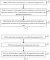
- Fig. 1 is a flow chart of a method for obtaining display data illustrated according to an example.
- the method may be applied to electronic devices, such as a smart phone, a smart bracelet, a tablet computer, a personal computer, a smart television and other devices.
- An Android system and an application program (APP) may be installed in the electronic devices.
- the method for obtaining display data includes step 11 to step 13.
- step 11 rendering data corresponding to an application program surface are obtained.
- an electronic device may detect operations by a user on a display screen of the electronic device in real time or according to a set cycle.
- the above operations may include but are not limited to: click, double-click, dragging, long press, etc.
- the electronic device may obtain the rendering data corresponding to the application program surface in response to detecting the operation of triggering the application program surface.
- the electronic device may obtain surface data corresponding to the application program surface.
- a corresponding surface of the application program surface is an initial surface, and a dimension of the initial surface is a first dimension.
- the surface data may include at least one of following images: a corresponding image (such as a last frame of image displayed) upon detecting the operation of triggering the application program surface, an image pre-stored locally, or an image set in an application program (such as an icon of the application program).
- Suitable surface data may be selected based on a specific scenario, and under a condition that display data of a masking layer can be generated, corresponding solutions fall into the protective scope of the disclosure.
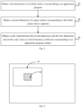
- step 21 when the operation of triggering the application program surface is detected, a buffer-type SurfaceControl module will be simultaneously created, the SurfaceControl module includes a buffer, and the buffer is a target buffer in subsequent step 23.
- the electronic device may obtain the rendering data by rendering the surface data.
- the rendering data are obtained by rendering the surface data through an interface API provided by a 2D hardware drawing module HWUI in the Android system, and the obtained rendering data are stored in a buffer corresponding to the 2D hardware drawing module HWUI.
- the electronic device may store the rendering data to the target buffer; and the target buffer is created upon detecting the operation of triggering the application program surface.
- the electronic device may bind rendering data drawn by the 2D hardware drawing module HWUI to the target buffer, such that an effect of storing the rendering data to the buffer in the SurfaceControl module is achieved.
- step 12 a transformation coefficient corresponding to the application program surface is obtained in response to detecting the operation of adjusting the dimension of the application program surface.
- the transformation coefficient may include at least one of following parameters: a scale coefficient, a rotation angle, or an offset distance.
- a technician may select a suitable transformation system according to the specific scenario, which is not limited here.
- the scale coefficient is a scale value between a dimension of the application program surface after adjustment and a dimension before adjustment. The solution is described by taking the scale coefficient as an example in subsequent examples.
- the electronic device may continue to detect the operations by the user on the display screen of the electronic device in real time or according to the set cycle.
- the above operations may include but are not limited to: click, double-click, dragging, long press, etc.
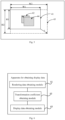
- the electronic device may obtain the first dimension of the initial surface corresponding to the application program in response to detecting the operation of triggering the application program surface, such as the first dimension of the initial surface 41 in Fig. 4 : a width W1 and a height HI.
- the initial surface 41 is generated when starting the application program in step 21.
- the electronic device may obtain a second dimension of a target surface corresponding to the initial surface that is adjusted.
- the initial surface 41 is amplified to the target surface 43 in a direction shown by v to obtain the second dimension of the target surface in Fig. 5 : a width W2 and a height H2.
- step 13 the display data of the corresponding masking layer of the application program surface are obtained according to the transformation coefficient and the rendering data.
- the electronic may obtain the display data of the corresponding masking layer of the application program surface according to the transformation coefficient and the rendering data.
- a display module in the electronic device may process the transformation coefficient and the rendering data, i.e. zoom the above rendering data according to the above transformation coefficient to obtain the display data.
- the display data are used for the corresponding masking layer of the application program surface, and the masking layer shown in Fig. 5 is finally formed, i.e. the image set in the application program, that is the icon of the application program, is displayed in the masking layer.
- the rendering data may be processed by adopting a preset filtering method (such as Gaussian Blur). Under a condition that processing of the rendering data can be implemented, corresponding solutions fall into the protective scope of the disclosure.
- a preset filtering method such as Gaussian Blur
- the rendering data corresponding to the application program surface may be obtained upon detecting the operation of triggering the application program surface; then the transformation coefficient corresponding to the application program surface may be obtained in response to detecting the operation of adjusting the dimension of the application program surface, the transformation coefficient being the scale value between the dimension of the application program surface after adjustment and the dimension before adjustment; and then the display data of the corresponding masking layer of the application program surface are obtained according to the transformation coefficient and the rendering data.
- the display data are obtained by adjusting the rendering data through the transformation coefficient, i.e. inter-process communication is not needed and communication time consumption can be reduced, which is conducive to avoiding or mitigating a phenomenon of display frame loss and improving a viewing experience.
- Superiorities of the method for obtaining display data provided by the example are described below in combination with an operation system of the electronic device.
- a solution of adding a masking layer in the example is a method for obtaining display data.
- Step 1 the user starts the application program (APP), and at the moment, the dimension of the application program surface is 3x3 cm.
- a SystemServer module in the operation system obtains the above dimension 3x3 cm.
- the buffer-type SurfaceControl module is created, and the size of the masking layer is 3x3 cm.
- the buffer may contain the following information: a picture, such as an RGB value, a text, and pixel point information.
- a masking layer is re-drawn on the buffer.
- Step 2 the user drags the above application program surface and amplifies it to a 6x6 cm target surface.
- a SystemServer module in the operation system obtains a dimension 6x6 cm of the target surface, and the SystemServer module obtains a scale value 200% between a length and a width, i.e. obtain the transformation coefficient corresponding to the masking layer.
- Step 3 the SystemServer module sends the above transformation coefficient 200% to the 2D hardware drawing module HWUI, and the 2D hardware drawing module HWUI sets a zooming coefficient. At the moment, the rendering data in the buffer are not changed.
- Step 4 a Display module of the system obtains buffer data and the transformation coefficient provided by step 2 to perform zooming processing, and uses processed display data to perform display.
- an example further provides an apparatus for obtaining display data.
- the apparatus includes:
- the rendering data obtaining module includes:
- the surface data include at least one of following images: a corresponding image upon detecting the operation of triggering the application program surface, an image pre-stored locally, or an image set in an application program.
- the transformation coefficient includes at least one of following parameters: a scale coefficient, a rotation angle, or an offset distance.
- the transformation coefficient obtaining module includes:
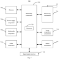
- Fig. 7 is a block diagram of an electronic device illustrated according to an example.
- the electronic device 700 may be a smart phone, a computer, a digital broadcasting terminal, a tablet device, a medical device, a fitness device, a personal digital assistant, etc.
- the electronic device 700 may include one or a plurality of the following components: a processing component 702, a memory 704, a power supply component 706, a multimedia component 708, an audio component 710, an input/output (I/O) interface 712, a sensor component 714, a communication component 716, and an image acquisition component 718.
- the processing component 702 generally controls overall operations of the electronic device 700, such as operations associated with display, telephone calls, data communications, camera operations, and recording operations.
- the processing component 702 may include one or a plurality of processors 720 to execute a computer program.
- the processing component 702 may include one or a plurality of modules to facilitate interaction between the processing component 702 and other components.
- the processing component 702 may include a multimedia module to facilitate interaction between the multimedia component 708 and the processing component 702.
- the memory 704 is configured to store various types of data to support the operations of the electronic device 700. Examples of these data include any application program or computer programs for method operating on the electronic device 700, contact data, phone book data, messages, pictures, videos, etc.
- the memory 704 may be implemented by any type of volatile or non-volatile storage device or their combination, such as a static random access memory (SRAM), an electrically erasable programmable read-only memory (EEPROM), an erasable programmable read-only memory (EPROM), a programmable read-only memory (PROM), a read-only memory (ROM), a magnetic memory, a flash memory, a magnetic disk or an optical disk.
- SRAM static random access memory
- EEPROM electrically erasable programmable read-only memory
- EPROM erasable programmable read-only memory
- PROM programmable read-only memory
- ROM read-only memory
- magnetic memory a magnetic memory
- flash memory a flash memory
- the power supply component 706 provides power for various components of the electronic device 700.
- the power supply component 706 may include a power management system, one or a plurality of power supplies, and other components associated with the generation, management, and distribution of power for the electronic device 700.
- the power supply component 706 may include a power supply chip, and a controller may communicate with the power supply chip to control the power supply chip to turn on or off a switching device, so that a battery supplies or does not supply power to a main board circuit.
- the multimedia component 708 includes a screen that provides an output interface between the electronic device 700 and a target object.
- the screen may include a liquid crystal display (LCD) and a touch panel (TP). If the screen includes the touch panel, the screen may be implemented as a touch screen to receive input information from the target object.
- the touch panel includes one or a plurality of touch sensors to sense touch, wipe, and gestures on the touch panel. The touch sensors may not only sense a boundary of a touch or wipe action, but also detect a duration and pressure associated with a touch or wipe operation.
- the audio component 710 is configured to output and/or input audio file information.
- the audio component 710 includes a microphone (MIC).
- the microphone is configured to receive external audio file information.
- the received audio file information may be further stored in the memory 704 or sent via the communication component 716.
- the audio component 710 further includes a speaker for outputting audio file information.
- the I/O interface 712 provides an interface between the processing component 702 and a peripheral interface module.
- the above-mentioned peripheral interface module may be a keyboard, a click wheel, a button, and the like.
- the sensor component 714 includes one or a plurality of sensors for providing the electronic device 700 with various aspects of state evaluation.
- the sensor component 714 may detect on/off status of the electronic device 700, or relative positioning of the components, such as a display screen and a keypad of the electronic device 700.
- the sensor component 714 may also detect a position change of the electronic device 700 or a component, presence or absence of contact between the target object and the electronic device 700, an orientation or acceleration/deceleration of the electronic device 700, and a temperature change of the electronic device 700.
- the sensor component 714 may include a magnetic sensor, a gyroscope, and a magnetic field sensor, where the magnetic field sensor includes at least one of: a Hall sensor, a thin film magnetoresistance sensor, and a magnetic liquid acceleration sensor.
- the communication component 716 is configured to facilitate wired or wireless communication between the electronic device 700 and other devices.
- the electronic device 700 may access a wireless network based on a communication standard, such as WiFi, 2G, 3G, 4G, 5G, or a combination of them.
- the communication component 716 receives broadcast information or broadcast-related information from an external broadcast management system via a broadcast channel.
- the communication component 716 also includes a near field communication (NFC) module to facilitate short-range communication.
- the NFC module may be implemented based on radio frequency identification (RFID) technology, Infrared Data Association (IrDA) technology, ultra-wideband (UWB) technology, Bluetooth (BT) technology and other technologies.
- RFID radio frequency identification
- IrDA Infrared Data Association
- UWB ultra-wideband
- Bluetooth Bluetooth
- the electronic device 700 may be implemented by one or more of an application specific integrated circuit (ASIC), a digital information processor (DSP), a digital information processing device (DSPD), a programmable logic device (PLD), a field programmable gate array (FPGA), a controller, a microcontroller, a microprocessor or other electronic elements.
- ASIC application specific integrated circuit
- DSP digital information processor
- DSPD digital information processing device
- PLD programmable logic device
- FPGA field programmable gate array
- controller a microcontroller, a microprocessor or other electronic elements.
- a non-transitory readable storage medium including an executable computer program is further provided, such as a memory 704 including instructions.
- the above executable computer program may be executed by a processor.
- the readable storage medium may be a ROM, a random access memory (RAM), a CD-ROM, a magnetic tape, a floppy disk, an optical data storage device, etc.
Landscapes
- Engineering & Computer Science (AREA)
- Theoretical Computer Science (AREA)
- General Engineering & Computer Science (AREA)
- Physics & Mathematics (AREA)
- General Physics & Mathematics (AREA)
- Human Computer Interaction (AREA)
- Software Systems (AREA)
- User Interface Of Digital Computer (AREA)
- Controls And Circuits For Display Device (AREA)
Applications Claiming Priority (1)
| Application Number | Priority Date | Filing Date | Title |
|---|---|---|---|
| CN202110886640.7A CN115934214A (zh) | 2021-08-03 | 2021-08-03 | 显示数据获取方法及装置、电子设备、存储介质 |
Publications (2)
| Publication Number | Publication Date |
|---|---|
| EP4130996A1 true EP4130996A1 (fr) | 2023-02-08 |
| EP4130996B1 EP4130996B1 (fr) | 2026-03-04 |
Family
ID=80449089
Family Applications (1)
| Application Number | Title | Priority Date | Filing Date |
|---|---|---|---|
| EP22153956.2A Active EP4130996B1 (fr) | 2021-08-03 | 2022-01-28 | Procédé permettant d'obtenir des données d'affichage, dispositif électronique et support de stockage |
Country Status (3)
| Country | Link |
|---|---|
| US (1) | US11733863B2 (fr) |
| EP (1) | EP4130996B1 (fr) |
| CN (1) | CN115934214A (fr) |
Families Citing this family (1)
| Publication number | Priority date | Publication date | Assignee | Title |
|---|---|---|---|---|
| CN117033834A (zh) * | 2023-08-25 | 2023-11-10 | 北京字跳网络技术有限公司 | 页面渲染方法、装置、计算机可读介质及电子设备 |
Citations (1)
| Publication number | Priority date | Publication date | Assignee | Title |
|---|---|---|---|---|
| US20170308988A1 (en) * | 2016-04-20 | 2017-10-26 | Mediatek Inc. | Graphics accelerator |
Family Cites Families (6)
| Publication number | Priority date | Publication date | Assignee | Title |
|---|---|---|---|---|
| JP2004178498A (ja) * | 2002-11-29 | 2004-06-24 | Trecenti Technologies Inc | 閲覧情報管理システムおよび管理方法 |
| US20070282673A1 (en) * | 2006-04-28 | 2007-12-06 | Lehman Brothers Inc. | Method and system for implementing portal |
| US20100057566A1 (en) * | 2008-09-03 | 2010-03-04 | Oded Itzhak | System and method for multiple layered pay-per-click advertisements |
| US20150143256A1 (en) * | 2013-11-20 | 2015-05-21 | Memoreze LLC | Interface for Interaction with a Compendium by Members of a Group |
| US10068912B1 (en) * | 2017-06-05 | 2018-09-04 | Cypress Semiconductor Corporation | Method of reducing charge loss in non-volatile memories |
| US11829225B2 (en) * | 2020-02-25 | 2023-11-28 | Intel Corporation | Partial panel screen dimming |
-
2021
- 2021-08-03 CN CN202110886640.7A patent/CN115934214A/zh active Pending
-
2022
- 2022-01-26 US US17/585,257 patent/US11733863B2/en active Active
- 2022-01-28 EP EP22153956.2A patent/EP4130996B1/fr active Active
Patent Citations (1)
| Publication number | Priority date | Publication date | Assignee | Title |
|---|---|---|---|---|
| US20170308988A1 (en) * | 2016-04-20 | 2017-10-26 | Mediatek Inc. | Graphics accelerator |
Non-Patent Citations (3)
| Title |
|---|
| ANONYMOUS: "android - Understanding Canvas and Surface concepts - Stack Overflow", 17 February 2017 (2017-02-17), XP055933969, Retrieved from the Internet <URL:https://stackoverflow.com/questions/4576909/understanding-canvas-and-surface-concepts> [retrieved on 20220621] * |
| CHRIS SIMMONDS: "The Android graphics path in depth The Android graphics path 1 Copyright ?2011-2014, 2net Limited", 12 November 2020 (2020-11-12), XP055933892, Retrieved from the Internet <URL:https://web.archive.org/web/20201112015536if_/https://elinux.org/images/2/2b/Android_graphics_path--chis_simmonds.pdf> [retrieved on 20220621] * |
| JACOB SU: "How did Android SurfaceView Works? | by Jacob su | Medium", 26 April 2020 (2020-04-26), XP055933962, Retrieved from the Internet <URL:https://medium.com/@zpcat/how-did-android-surfaceview-works-33afb7111b69> [retrieved on 20220621] * |
Also Published As
| Publication number | Publication date |
|---|---|
| US11733863B2 (en) | 2023-08-22 |
| EP4130996B1 (fr) | 2026-03-04 |
| US20230045025A1 (en) | 2023-02-09 |
| CN115934214A (zh) | 2023-04-07 |
Similar Documents
| Publication | Publication Date | Title |
|---|---|---|
| US11183153B1 (en) | Image display method and device, electronic device, and storage medium | |
| EP3182716A1 (fr) | Procédé et dispositif d'affichage vidéo | |
| US9858885B2 (en) | Method and device for reducing display brightness | |
| EP3173923A1 (fr) | Procédé et dispositif d'affichage d'images | |
| US20180365200A1 (en) | Method, device, electric device and computer-readable storage medium for updating page | |
| CN104238911B (zh) | 加载图标显示方法和装置 | |
| US20180204500A1 (en) | Method and device for enhancing contrast | |
| CN105094539B (zh) | 参考信息显示方法和装置 | |
| CN105389083B (zh) | 大字体实现方法和装置、智能终端 | |
| CN111552532A (zh) | 弹窗控制方法、装置、电子设备及存储介质 | |
| US11221734B2 (en) | Punch-hole screen display method and apparatus | |
| US20220308752A1 (en) | Interface display method and apparatus of an application | |
| US20190012299A1 (en) | Displaying page | |
| EP4130996A1 (fr) | Procédé permettant d'obtenir des données d'affichage, dispositif électronique et support de stockage | |
| US20210120276A1 (en) | Screen display device, method and device for controlling screen display and storage medium | |
| CN115798394B (zh) | 亮度调整方法、装置及存储介质 | |
| CN108804187A (zh) | 界面窗口的设置方法及装置 | |
| CN105469411B (zh) | 用于检测图像清晰度的方法、装置及终端 | |
| CN113918107B (zh) | 一种显示方法和装置 | |
| US11755177B2 (en) | Method and apparatus for adjusting window, electronic device, and computer readable storage medium | |
| CN105930034A (zh) | 显示对话框的方法和装置 | |
| CN111383568A (zh) | 显示控制方法和装置、电子设备以及计算机可读存储介质 | |
| CN117836847A (zh) | 屏幕亮度的调节方法、装置、设备及存储介质 | |
| US20220310034A1 (en) | Method and device for adjusting display brightness, mobile terminal and storage medium | |
| CN112464125B (zh) | 页面展示方法及装置、电子设备、存储介质 |
Legal Events
| Date | Code | Title | Description |
|---|---|---|---|
| PUAI | Public reference made under article 153(3) epc to a published international application that has entered the european phase |
Free format text: ORIGINAL CODE: 0009012 |
|
| STAA | Information on the status of an ep patent application or granted ep patent |
Free format text: STATUS: REQUEST FOR EXAMINATION WAS MADE |
|
| 17P | Request for examination filed |
Effective date: 20220128 |
|
| AK | Designated contracting states |
Kind code of ref document: A1 Designated state(s): AL AT BE BG CH CY CZ DE DK EE ES FI FR GB GR HR HU IE IS IT LI LT LU LV MC MK MT NL NO PL PT RO RS SE SI SK SM TR |
|
| RBV | Designated contracting states (corrected) |
Designated state(s): AL AT BE BG CH CY CZ DE DK EE ES FI FR GB GR HR HU IE IS IT LI LT LU LV MC MK MT NL NO PL PT RO RS SE SI SK SM TR |
|
| STAA | Information on the status of an ep patent application or granted ep patent |
Free format text: STATUS: EXAMINATION IS IN PROGRESS |
|
| 17Q | First examination report despatched |
Effective date: 20240312 |
|
| REG | Reference to a national code |
Ref country code: DE Ref legal event code: R079 Free format text: PREVIOUS MAIN CLASS: G06F0009451000 Ipc: G06T0003400000 Ref document number: 602022031436 Country of ref document: DE |
|
| GRAP | Despatch of communication of intention to grant a patent |
Free format text: ORIGINAL CODE: EPIDOSNIGR1 |
|
| STAA | Information on the status of an ep patent application or granted ep patent |
Free format text: STATUS: GRANT OF PATENT IS INTENDED |
|
| RIC1 | Information provided on ipc code assigned before grant |
Ipc: G06T 3/40 20060101AFI20250703BHEP Ipc: G06F 9/451 20180101ALI20250703BHEP |
|
| INTG | Intention to grant announced |
Effective date: 20250711 |
|
| GRAJ | Information related to disapproval of communication of intention to grant by the applicant or resumption of examination proceedings by the epo deleted |
Free format text: ORIGINAL CODE: EPIDOSDIGR1 |
|
| STAA | Information on the status of an ep patent application or granted ep patent |
Free format text: STATUS: EXAMINATION IS IN PROGRESS |
|
| GRAP | Despatch of communication of intention to grant a patent |
Free format text: ORIGINAL CODE: EPIDOSNIGR1 |
|
| STAA | Information on the status of an ep patent application or granted ep patent |
Free format text: STATUS: GRANT OF PATENT IS INTENDED |
|
| INTG | Intention to grant announced |
Effective date: 20250923 |
|
| GRAS | Grant fee paid |
Free format text: ORIGINAL CODE: EPIDOSNIGR3 |
|
| GRAA | (expected) grant |
Free format text: ORIGINAL CODE: 0009210 |
|
| STAA | Information on the status of an ep patent application or granted ep patent |
Free format text: STATUS: THE PATENT HAS BEEN GRANTED |
|
| AK | Designated contracting states |
Kind code of ref document: B1 Designated state(s): AL AT BE BG CH CY CZ DE DK EE ES FI FR GB GR HR HU IE IS IT LI LT LU LV MC MK MT NL NO PL PT RO RS SE SI SK SM TR |
|
| REG | Reference to a national code |
Ref country code: CH Ref legal event code: F10 Free format text: ST27 STATUS EVENT CODE: U-0-0-F10-F00 (AS PROVIDED BY THE NATIONAL OFFICE) Effective date: 20260304 Ref country code: GB Ref legal event code: FG4D |
|
| REG | Reference to a national code |
Ref country code: IE Ref legal event code: FG4D |
|
| REG | Reference to a national code |
Ref country code: DE Ref legal event code: R096 Ref document number: 602022031436 Country of ref document: DE |