EP4131238A1 - Pixelschaltung und ansteuerungsverfahren dafür, und anzeigevorrichtung und ansteuerungsverfahren dafür - Google Patents
Pixelschaltung und ansteuerungsverfahren dafür, und anzeigevorrichtung und ansteuerungsverfahren dafür Download PDFInfo
- Publication number
- EP4131238A1 EP4131238A1 EP20924970.5A EP20924970A EP4131238A1 EP 4131238 A1 EP4131238 A1 EP 4131238A1 EP 20924970 A EP20924970 A EP 20924970A EP 4131238 A1 EP4131238 A1 EP 4131238A1
- Authority
- EP
- European Patent Office
- Prior art keywords
- circuit
- light
- transistor
- electrically connected
- control signal
- Prior art date
- Legal status (The legal status is an assumption and is not a legal conclusion. Google has not performed a legal analysis and makes no representation as to the accuracy of the status listed.)
- Granted
Links
Images






Classifications
-
- G—PHYSICS
- G09—EDUCATION; CRYPTOGRAPHY; DISPLAY; ADVERTISING; SEALS
- G09G—ARRANGEMENTS OR CIRCUITS FOR CONTROL OF INDICATING DEVICES USING STATIC MEANS TO PRESENT VARIABLE INFORMATION
- G09G3/00—Control arrangements or circuits, of interest only in connection with visual indicators other than cathode-ray tubes
- G09G3/20—Control arrangements or circuits, of interest only in connection with visual indicators other than cathode-ray tubes for presentation of an assembly of a number of characters, e.g. a page, by composing the assembly by combination of individual elements arranged in a matrix no fixed position being assigned to or needed to be assigned to the individual characters or partial characters
- G09G3/22—Control arrangements or circuits, of interest only in connection with visual indicators other than cathode-ray tubes for presentation of an assembly of a number of characters, e.g. a page, by composing the assembly by combination of individual elements arranged in a matrix no fixed position being assigned to or needed to be assigned to the individual characters or partial characters using controlled light sources
- G09G3/30—Control arrangements or circuits, of interest only in connection with visual indicators other than cathode-ray tubes for presentation of an assembly of a number of characters, e.g. a page, by composing the assembly by combination of individual elements arranged in a matrix no fixed position being assigned to or needed to be assigned to the individual characters or partial characters using controlled light sources using electroluminescent panels
- G09G3/32—Control arrangements or circuits, of interest only in connection with visual indicators other than cathode-ray tubes for presentation of an assembly of a number of characters, e.g. a page, by composing the assembly by combination of individual elements arranged in a matrix no fixed position being assigned to or needed to be assigned to the individual characters or partial characters using controlled light sources using electroluminescent panels semiconductive, e.g. using light-emitting diodes [LED]
- G09G3/3208—Control arrangements or circuits, of interest only in connection with visual indicators other than cathode-ray tubes for presentation of an assembly of a number of characters, e.g. a page, by composing the assembly by combination of individual elements arranged in a matrix no fixed position being assigned to or needed to be assigned to the individual characters or partial characters using controlled light sources using electroluminescent panels semiconductive, e.g. using light-emitting diodes [LED] organic, e.g. using organic light-emitting diodes [OLED]
- G09G3/3225—Control arrangements or circuits, of interest only in connection with visual indicators other than cathode-ray tubes for presentation of an assembly of a number of characters, e.g. a page, by composing the assembly by combination of individual elements arranged in a matrix no fixed position being assigned to or needed to be assigned to the individual characters or partial characters using controlled light sources using electroluminescent panels semiconductive, e.g. using light-emitting diodes [LED] organic, e.g. using organic light-emitting diodes [OLED] using an active matrix
- G09G3/3233—Control arrangements or circuits, of interest only in connection with visual indicators other than cathode-ray tubes for presentation of an assembly of a number of characters, e.g. a page, by composing the assembly by combination of individual elements arranged in a matrix no fixed position being assigned to or needed to be assigned to the individual characters or partial characters using controlled light sources using electroluminescent panels semiconductive, e.g. using light-emitting diodes [LED] organic, e.g. using organic light-emitting diodes [OLED] using an active matrix with pixel circuitry controlling the current through the light-emitting element
-
- G—PHYSICS
- G09—EDUCATION; CRYPTOGRAPHY; DISPLAY; ADVERTISING; SEALS
- G09G—ARRANGEMENTS OR CIRCUITS FOR CONTROL OF INDICATING DEVICES USING STATIC MEANS TO PRESENT VARIABLE INFORMATION
- G09G3/00—Control arrangements or circuits, of interest only in connection with visual indicators other than cathode-ray tubes
- G09G3/20—Control arrangements or circuits, of interest only in connection with visual indicators other than cathode-ray tubes for presentation of an assembly of a number of characters, e.g. a page, by composing the assembly by combination of individual elements arranged in a matrix no fixed position being assigned to or needed to be assigned to the individual characters or partial characters
- G09G3/22—Control arrangements or circuits, of interest only in connection with visual indicators other than cathode-ray tubes for presentation of an assembly of a number of characters, e.g. a page, by composing the assembly by combination of individual elements arranged in a matrix no fixed position being assigned to or needed to be assigned to the individual characters or partial characters using controlled light sources
- G09G3/30—Control arrangements or circuits, of interest only in connection with visual indicators other than cathode-ray tubes for presentation of an assembly of a number of characters, e.g. a page, by composing the assembly by combination of individual elements arranged in a matrix no fixed position being assigned to or needed to be assigned to the individual characters or partial characters using controlled light sources using electroluminescent panels
- G09G3/32—Control arrangements or circuits, of interest only in connection with visual indicators other than cathode-ray tubes for presentation of an assembly of a number of characters, e.g. a page, by composing the assembly by combination of individual elements arranged in a matrix no fixed position being assigned to or needed to be assigned to the individual characters or partial characters using controlled light sources using electroluminescent panels semiconductive, e.g. using light-emitting diodes [LED]
- G09G3/3208—Control arrangements or circuits, of interest only in connection with visual indicators other than cathode-ray tubes for presentation of an assembly of a number of characters, e.g. a page, by composing the assembly by combination of individual elements arranged in a matrix no fixed position being assigned to or needed to be assigned to the individual characters or partial characters using controlled light sources using electroluminescent panels semiconductive, e.g. using light-emitting diodes [LED] organic, e.g. using organic light-emitting diodes [OLED]
- G09G3/3225—Control arrangements or circuits, of interest only in connection with visual indicators other than cathode-ray tubes for presentation of an assembly of a number of characters, e.g. a page, by composing the assembly by combination of individual elements arranged in a matrix no fixed position being assigned to or needed to be assigned to the individual characters or partial characters using controlled light sources using electroluminescent panels semiconductive, e.g. using light-emitting diodes [LED] organic, e.g. using organic light-emitting diodes [OLED] using an active matrix
- G09G3/3258—Control arrangements or circuits, of interest only in connection with visual indicators other than cathode-ray tubes for presentation of an assembly of a number of characters, e.g. a page, by composing the assembly by combination of individual elements arranged in a matrix no fixed position being assigned to or needed to be assigned to the individual characters or partial characters using controlled light sources using electroluminescent panels semiconductive, e.g. using light-emitting diodes [LED] organic, e.g. using organic light-emitting diodes [OLED] using an active matrix with pixel circuitry controlling the voltage across the light-emitting element
-
- G—PHYSICS
- G09—EDUCATION; CRYPTOGRAPHY; DISPLAY; ADVERTISING; SEALS
- G09G—ARRANGEMENTS OR CIRCUITS FOR CONTROL OF INDICATING DEVICES USING STATIC MEANS TO PRESENT VARIABLE INFORMATION
- G09G2300/00—Aspects of the constitution of display devices
- G09G2300/08—Active matrix structure, i.e. with use of active elements, inclusive of non-linear two terminal elements, in the pixels together with light emitting or modulating elements
- G09G2300/0809—Several active elements per pixel in active matrix panels
- G09G2300/0819—Several active elements per pixel in active matrix panels used for counteracting undesired variations, e.g. feedback or autozeroing
-
- G—PHYSICS
- G09—EDUCATION; CRYPTOGRAPHY; DISPLAY; ADVERTISING; SEALS
- G09G—ARRANGEMENTS OR CIRCUITS FOR CONTROL OF INDICATING DEVICES USING STATIC MEANS TO PRESENT VARIABLE INFORMATION
- G09G2300/00—Aspects of the constitution of display devices
- G09G2300/08—Active matrix structure, i.e. with use of active elements, inclusive of non-linear two terminal elements, in the pixels together with light emitting or modulating elements
- G09G2300/0809—Several active elements per pixel in active matrix panels
- G09G2300/0842—Several active elements per pixel in active matrix panels forming a memory circuit, e.g. a dynamic memory with one capacitor
- G09G2300/0852—Several active elements per pixel in active matrix panels forming a memory circuit, e.g. a dynamic memory with one capacitor being a dynamic memory with more than one capacitor
-
- G—PHYSICS
- G09—EDUCATION; CRYPTOGRAPHY; DISPLAY; ADVERTISING; SEALS
- G09G—ARRANGEMENTS OR CIRCUITS FOR CONTROL OF INDICATING DEVICES USING STATIC MEANS TO PRESENT VARIABLE INFORMATION
- G09G2300/00—Aspects of the constitution of display devices
- G09G2300/08—Active matrix structure, i.e. with use of active elements, inclusive of non-linear two terminal elements, in the pixels together with light emitting or modulating elements
- G09G2300/0809—Several active elements per pixel in active matrix panels
- G09G2300/0842—Several active elements per pixel in active matrix panels forming a memory circuit, e.g. a dynamic memory with one capacitor
- G09G2300/0861—Several active elements per pixel in active matrix panels forming a memory circuit, e.g. a dynamic memory with one capacitor with additional control of the display period without amending the charge stored in a pixel memory, e.g. by means of additional select electrodes
-
- G—PHYSICS
- G09—EDUCATION; CRYPTOGRAPHY; DISPLAY; ADVERTISING; SEALS
- G09G—ARRANGEMENTS OR CIRCUITS FOR CONTROL OF INDICATING DEVICES USING STATIC MEANS TO PRESENT VARIABLE INFORMATION
- G09G2300/00—Aspects of the constitution of display devices
- G09G2300/08—Active matrix structure, i.e. with use of active elements, inclusive of non-linear two terminal elements, in the pixels together with light emitting or modulating elements
- G09G2300/0876—Supplementary capacities in pixels having special driving circuits and electrodes instead of being connected to common electrode or ground; Use of additional capacitively coupled compensation electrodes
-
- G—PHYSICS
- G09—EDUCATION; CRYPTOGRAPHY; DISPLAY; ADVERTISING; SEALS
- G09G—ARRANGEMENTS OR CIRCUITS FOR CONTROL OF INDICATING DEVICES USING STATIC MEANS TO PRESENT VARIABLE INFORMATION
- G09G2310/00—Command of the display device
- G09G2310/02—Addressing, scanning or driving the display screen or processing steps related thereto
- G09G2310/0243—Details of the generation of driving signals
- G09G2310/0251—Precharge or discharge of pixel before applying new pixel voltage
-
- G—PHYSICS
- G09—EDUCATION; CRYPTOGRAPHY; DISPLAY; ADVERTISING; SEALS
- G09G—ARRANGEMENTS OR CIRCUITS FOR CONTROL OF INDICATING DEVICES USING STATIC MEANS TO PRESENT VARIABLE INFORMATION
- G09G2310/00—Command of the display device
- G09G2310/06—Details of flat display driving waveforms
- G09G2310/061—Details of flat display driving waveforms for resetting or blanking
-
- G—PHYSICS
- G09—EDUCATION; CRYPTOGRAPHY; DISPLAY; ADVERTISING; SEALS
- G09G—ARRANGEMENTS OR CIRCUITS FOR CONTROL OF INDICATING DEVICES USING STATIC MEANS TO PRESENT VARIABLE INFORMATION
- G09G2310/00—Command of the display device
- G09G2310/08—Details of timing specific for flat panels, other than clock recovery
-
- G—PHYSICS
- G09—EDUCATION; CRYPTOGRAPHY; DISPLAY; ADVERTISING; SEALS
- G09G—ARRANGEMENTS OR CIRCUITS FOR CONTROL OF INDICATING DEVICES USING STATIC MEANS TO PRESENT VARIABLE INFORMATION
- G09G2320/00—Control of display operating conditions
- G09G2320/02—Improving the quality of display appearance
- G09G2320/0209—Crosstalk reduction, i.e. to reduce direct or indirect influences of signals directed to a certain pixel of the displayed image on other pixels of said image, inclusive of influences affecting pixels in different frames or fields or sub-images which constitute a same image, e.g. left and right images of a stereoscopic display
- G09G2320/0214—Crosstalk reduction, i.e. to reduce direct or indirect influences of signals directed to a certain pixel of the displayed image on other pixels of said image, inclusive of influences affecting pixels in different frames or fields or sub-images which constitute a same image, e.g. left and right images of a stereoscopic display with crosstalk due to leakage current of pixel switch in active matrix panels
-
- G—PHYSICS
- G09—EDUCATION; CRYPTOGRAPHY; DISPLAY; ADVERTISING; SEALS
- G09G—ARRANGEMENTS OR CIRCUITS FOR CONTROL OF INDICATING DEVICES USING STATIC MEANS TO PRESENT VARIABLE INFORMATION
- G09G2320/00—Control of display operating conditions
- G09G2320/02—Improving the quality of display appearance
- G09G2320/0233—Improving the luminance or brightness uniformity across the screen
-
- G—PHYSICS
- G09—EDUCATION; CRYPTOGRAPHY; DISPLAY; ADVERTISING; SEALS
- G09G—ARRANGEMENTS OR CIRCUITS FOR CONTROL OF INDICATING DEVICES USING STATIC MEANS TO PRESENT VARIABLE INFORMATION
- G09G2320/00—Control of display operating conditions
- G09G2320/02—Improving the quality of display appearance
- G09G2320/029—Improving the quality of display appearance by monitoring one or more pixels in the display panel, e.g. by monitoring a fixed reference pixel
- G09G2320/0295—Improving the quality of display appearance by monitoring one or more pixels in the display panel, e.g. by monitoring a fixed reference pixel by monitoring each display pixel
-
- G—PHYSICS
- G09—EDUCATION; CRYPTOGRAPHY; DISPLAY; ADVERTISING; SEALS
- G09G—ARRANGEMENTS OR CIRCUITS FOR CONTROL OF INDICATING DEVICES USING STATIC MEANS TO PRESENT VARIABLE INFORMATION
- G09G2320/00—Control of display operating conditions
- G09G2320/04—Maintaining the quality of display appearance
- G09G2320/043—Preventing or counteracting the effects of ageing
-
- G—PHYSICS
- G09—EDUCATION; CRYPTOGRAPHY; DISPLAY; ADVERTISING; SEALS
- G09G—ARRANGEMENTS OR CIRCUITS FOR CONTROL OF INDICATING DEVICES USING STATIC MEANS TO PRESENT VARIABLE INFORMATION
- G09G2320/00—Control of display operating conditions
- G09G2320/04—Maintaining the quality of display appearance
- G09G2320/043—Preventing or counteracting the effects of ageing
- G09G2320/045—Compensation of drifts in the characteristics of light emitting or modulating elements
Definitions
- Embodiments of the present disclosure relate to the field of display technology, in particular to a pixel circuit and a driving method thereof, a display device and a driving method thereof.
- OLEDs organic light-emitting diodes
- DTFTs driving TFTs
- OLED devices may deteriorate due to device aging after long-term use, resulting in image quality degradation problems such as afterimages during display.
- Embodiments of the present disclosure provide a pixel circuit and a driving method thereof, as well as a display device and a driving method thereof.
- a pixel circuit comprising: a plurality of pixel units arranged in a matrix, wherein each pixel unit comprises a light-emitting element and a pixel driving circuit for driving the light-emitting element to emit light, and the pixel driving circuit and the light-emitting element are electrically connected to a first node; a first compensation sub-circuit electrically connected to each pixel driving circuit in each of the plurality of pixel units, wherein the first compensation sub-circuit is configured to provide an initialization signal to the pixel driving circuit, and to obtain a voltage at the first node when the light-emitting element emits light via the pixel driving circuit, and to generate a compensation data signal based on the voltage at the first node; and a second compensation sub-circuit electrically connected to each pixel driving circuit in each of the plurality of pixel units and configured to keep the voltage at the first node within a set operating voltage range of the light-emitting element, where
- the first compensation sub-circuit comprises: a switching sub-circuit configured to receive a first switching signal and a second switching signal, and to output the initialization signal at an output terminal of the switching sub-circuit under the control of the first switching signal and keep the output terminal in a floating state under the control of the second switching signal; a sampling sub-circuit configured to obtain the voltage at the first node while the output terminal is kept in the floating state; and a data compensation sub-circuit configured to generate the compensation data signal based on a preset compensation model and the voltage at the first node.
- the switching sub-circuit comprises a first transistor, a second transistor, and a third transistor, wherein a gate of the first transistor is electrically connected to receive the first switching signal, a first electrode of the first transistor is electrically connected to receive the initialization signal, and a second electrode of the first transistor is electrically connected to a second electrode of the second transistor and serve as the output terminal; a gate of the second transistor is electrically connected to receive the second switching signal, and a first electrode of the second transistor is electrically connected to a first electrode of the third transistor; a gate of the third transistor is electrically connected to receive a sampling control signal, and a second electrode of the third transistor is electrically connected to the sampling sub-circuit.
- the pixel driving circuit comprises: a driving sub-circuit configured to generate a current for causing the light-emitting element to emit light; a light emission control sub-circuit electrically connected to the light-emitting element and the driving sub-circuit, and configured to receive a first control signal and supply a current for causing the light-emitting element to emit light to the light-emitting element under the control of the first control signal; a driving control sub-circuit electrically connected to the driving sub-circuit, and configured to receive the compensation data signal and a second control signal, and to provide the compensation data signal to the driving sub-circuit under the control of the second control signal; and a reset sub-circuit electrically connected to the driving sub-circuit and the first compensation sub-circuit, and configured to receive a third control signal and a fourth control signal, and to apply the initialization signal provided by the first compensation sub-circuit to the first node under the control of the third control signal and the fourth control signal or to output the voltage at the first node
- the driving sub-circuit comprises a driving transistor, a fourth transistor and a storage capacitor, wherein a gate of the driving transistor is electrically connected to a first end of the storage capacitor, a drain of the driving transistor and the light emission control sub-circuit are electrically connected to a second node, and a source of the driving transistor and the light emission control sub-circuit are electrically connected to a third node; a gate of the fourth transistor is electrically connected to receive the second control signal, a first electrode of the fourth transistor is electrically connected to the first end of the storage capacitor, and a second electrode of the fourth transistor is electrically connected to the second node; a second end of the storage capacitor is electrically connected to the first node.
- the light emission control sub-circuit comprises a fifth transistor and a sixth transistor, wherein a gate of the fifth transistor is electrically connected to receive the first control signal, a first electrode of the fifth transistor is electrically connected to receive a first voltage signal, and a second electrode of the fifth transistor is electrically connected to the second node; a gate of the sixth transistor is electrically connected to receive the first control signal, a first electrode of the sixth transistor is electrically connected to the third node, and a second electrode of the sixth transistor is electrically connected to the first node.
- the driving control sub-circuit comprises a seventh transistor, a gate of the seventh transistor is electrically connected to receive the second control signal, a first electrode of the seventh transistor is electrically connected to receive the compensation data signal, and a second electrode of the seventh transistor is electrically connected to the third node.
- the second compensation sub-circuit comprises a plurality of compensation capacitors which correspond to respective pixel driving circuits, and a first end of each of the compensation capacitors is electrically connected to the first node, and the second end of each of the compensation capacitors is electrically connected to the gate of the seventh transistor.
- the reset sub-circuit comprises an eighth transistor and a ninth transistor, wherein a gate of the eighth transistor is electrically connected to receive a third control signal, a first electrode of the eighth transistor is electrically connected to the first node, and a second electrode of the eighth transistor is electrically connected to the output terminal of the switching sub-circuit; a gate of the ninth transistor is electrically connected to receive a fourth control signal, a first electrode of the ninth transistor is electrically connected to receive the first voltage signal, and a second electrode of the ninth transistor is electrically connected to the first end of the storage capacitor.
- a display device comprising the pixel circuit according to the above embodiments is provided.
- a method for driving a pixel circuit comprising: compensating a threshold voltage of the pixel driving circuit, so as to eliminate influence of the threshold voltage on a current flowing through the light-emitting element; generating the compensation data signal by using the first compensation sub-circuit; and driving the light-emitting element in each pixel unit to emit light based on the compensation data signal.
- the compensation data signal is generated based on light-emitting brightness of a selected light-emitting element before driving the light-emitting element in each pixel unit to emit light.
- the compensation data signal is generated based on light-emitting brightness of a light-emitting element in each of selected pixel units or based on the light-emitting brightness of the light-emitting element in each pixel unit.
- generating the compensation data signal by using the first compensation sub-circuit comprises: in a first sampling period, providing a second switching signal, a first control signal, and a third control signal which all have a first level, and providing a first switching signal, a sampling control signal, a second control signal, and a fourth control signal which all have a second level; and in a second sampling period, providing the second switching signal, the sampling control signal, the first control signal, and the third control signal which all have the first level, and providing the first switching signal, the second control signal, and the fourth control signal which all have the second level.
- driving the light-emitting element in each pixel unit to emit light based on the compensation data signal comprises: in a first driving period, providing the first switching signal, the third control signal, and the fourth control signal which all have the first level, and providing the second switching signal, the first control signal, and the second control signal which all have the second level; in a second driving period, providing the first switching signal, the second control signal, and the third control signal which all have the first level, and providing the second switching signal, the first control signal, and the fourth control signal which all have the second level; and in a third driving period, providing the first switching signal and the first control signal which both have the first level, and providing the second switching signal, the second control signal, the third control signal, and the fourth control signal which all have the second level.
- a display method by using a display device comprising: generating the compensation data signal by using the first compensation sub-circuit of the pixel circuit; and driving the light-emitting element in each pixel unit to emit light based on the compensation data signal by using the pixel units of the pixel circuit.
- the first compensation sub-circuit before driving the light-emitting element in each pixel unit to emit light, the first compensation sub-circuit generates the compensation data signal based on light-emitting brightness of a selected light-emitting element.
- the first compensation sub-circuit in a process of driving the light-emitting element in each pixel unit to emit light, the first compensation sub-circuit generates the compensation data signal based on light-emitting brightness of the light-emitting element in each pixel unit.
- a term "electrically connected” may mean that two components are directly electrically connected, or may mean that two components are electrically connected via one or more other components. In addition, these two components may be electrically connected or coupled in a wired or wireless manner.
- Transistors used in the embodiments of the present disclosure may all be thin film transistors or field effect transistors or other devices with the same characteristics. According to the role in the circuit, the transistors used in the embodiments of the present disclosure are mainly switching transistors. Since a source and a drain of a thin film transistor used here are symmetrical, the source and the drain may be interchanged. In the embodiments of the present disclosure, one of the source and the drain is called a first electrode, and the other of the source and the drain is called a second electrode.
- a driving transistor is described as an N-type thin film transistor, and other transistors are of the same type as the driving transistor or are of different type from the driving transistor according to the circuit design.
- the driving transistor may also be shown as a P-type thin film transistor.
- the technology solutions of the present disclosure may also be realized by correspondingly changing the types of other transistors and inverting each drive signal and level signal (and/or making other additional adaptive modifications).
- first level and second level are only configured to distinguish two levels with different amplitudes.
- the "first level” may be a high level
- the “second level” may be a low level.
- the driving transistor is exemplified as an N-type thin film transistor
- the "first level” is exemplified as a high level
- the “second level” is exemplified as a low level.
- the driving transistor DTFT made by the LTPS process is usually configured to provide a current required for the OLED to emit light.
- the LTPS process is generally unable to maintain stability, under effects of excimer laser annealing (ELA) crystallization, long-term stress, temperature changes and the like, the threshold voltage Vth and mobility of the transistor may shift.
- ELA excimer laser annealing
- OLED devices may undergo aging after long-term use, which leads to degradation of device characteristics, so that a preset voltage and current cannot be maintained.
- FIG. 1 shows a schematic block diagram of a pixel circuit 10 according to embodiments of the present disclosure.
- the pixel circuit 10 includes a plurality of pixel units 11, and the plurality of pixel units 11 are arranged in the form of an m ⁇ n matrix, wherein m and n are natural numbers.
- Each pixel unit 11 may include a pixel driving circuit 111 and a light-emitting element 112, wherein the pixel driving circuit 111 is configured to drive the light-emitting element 112 to emit light.
- the pixel driving circuit 111 and the light-emitting element 112 are electrically connected to a first node N1.
- the light-emitting element 112 is exemplified as an OLED element, but this is not to limit the present disclosure. In other embodiments, the light-emitting element 112 may also be other current-driven light-emitting elements.
- the pixel circuit 10 may further include a first compensation sub-circuit 12.
- the first compensation sub-circuit 12 is electrically connected to each pixel driving circuit 111 in the plurality of pixel units 11.
- the first compensation sub-circuit 12 is configured to provide an initialization signal to the pixel driving circuit 111, and obtain a voltage at the first node N1 when the light-emitting element 112 emits light via the pixel driving circuit 111, and generate a compensation data signal based on the voltage at the first node N1.
- the first compensation sub-circuit 12 includes wirings Vref/Sens(1), Vref/Sens(2)..., Vref/Sens(n), that is, there are n wirings in total, corresponding to n columns of pixel units 11 respectively.
- Each of the wirings Vref/Sens(1), Vref/Sens(2)..., Vref/Sens(n) may be used as an input wiring to provide an initialization signal Vref to the pixel driving circuit 111, or may be used as an output wiring to obtain the voltage at the first node N1 when the light-emitting element 112 emits light via the pixel driving circuit 111.
- the first compensation sub-circuit 12 also includes wirings Da 1 , Da 2 , ..., Da n , that is, there are n wirings in total.
- the wirings Da 1 , Da 2 , ..., Da n may be used as data lines of the pixel circuit 10, which corresponds to n columns of pixel units 11, respectively.
- the pixel driving circuit 111 is provided with a data signal compensated by the first compensation sub-circuit 12.
- wirings G 1 , G 2 , G 3 , ..., G m are also shown, that is, there are m wirings.
- G 1 , G 2 , G 3 , ..., G m are gate lines of the pixel circuit 10, and they correspond to m rows of pixel units 11, respectively.
- the pixel driving circuit 111 is further configured to initialize the first node N1 based on the initialization signal Vref, and drive the light-emitting element 112 to emit light by using the compensation data signals Da 1 , Da 2 ,..., Da n .
- the pixel circuit 10 may further include second compensation sub-circuits 13, and the second compensation sub-circuits 13 are electrically connected to respective pixel driving circuits 111 in the plurality of pixel units 11.
- the second compensation sub-circuits 13 are configured to keep the voltage at the first node N1 within a set operating voltage range of the light-emitting element 112 at all times.
- FIG. 2 shows a schematic block diagram of the first compensation sub-circuit 20 according to embodiments of the present disclosure.
- the first compensation sub-circuit 20 may include a switching sub-circuit 21, a sampling sub-circuit 22 and a data compensation sub-circuit 23.
- the switching sub-circuit 21 is configured to receive a first switching signal SW1 and a second switching signal SW2, and to output the initialization signal at an output terminal of the switching sub-circuit 21 under the control of the first switching signal SW1, and to keep the output terminal of the switching sub-circuit 21 in a floating state under the control of the switching signal SW2.
- the output terminal Vref/Sens(k) of the switching sub-circuit 21 connected to the k th column of the pixel units is taken as an example for description, wherein k is a natural number and 1 ⁇ k ⁇ n.
- a pixel driving circuit of the k th column of the pixel units is shown in a dashed frame.
- the output terminal Vref/Sens(k) outputs a signal Vref.
- the output terminal Vref/Sens(k) Under the control of the second switching signal SW2, the output terminal Vref/Sens(k) is kept in a floating state, and the voltage at the first node N1 in the k th column of the pixel units connected to the output terminal Vref/Sens(k) may be obtained via the output terminal Vref/Sens(k).
- the sampling sub-circuit 22 is configured to obtain the voltage at the first node N1 while the output terminal of the switching sub-circuit 21 is kept in a floating state.
- the sampling sub-circuit 22 may be an analog-to-digital converter ADC.
- the analog-to-digital converter ADC is electrically connected to the output terminal Vref/Sens(k), so that the voltage at the first node N1 is collected by the analog-to-digital converter ADC.
- the sampling sub-circuit 22 may also be a sampling unit formed by a dedicated integrated circuit IC, which are not limited in the embodiments of the present disclosure.
- the data compensation sub-circuit 23 is configured to generate a compensation data signal Da k based on a preset compensation model and the voltage at the first node N1.
- the data compensation sub-circuit 23 has n output terminals, which correspond to the n columns of pixel units 11 respectively, and the compensation data signal Da k is output through the output terminal electrically connected to the k th column of pixel units.
- a circuit structure for realizing the preset compensation model is built in the data compensation sub-circuit 23, wherein the compensation model may be established according to an aging curve of the OLED, and may compensate the aging of the OLED.
- the compensation model may compare the collected voltage at the first node N1 with the expected voltage of the OLED under the brightness, so that the compensation signal is obtained according to the compensation model, and further the voltage is fed back to the data signal to compensate the brightness of the OLED.
- the present disclosure does not limit the specific implementation of the compensation model. According to the concept of the present disclosure, any solutions which may compensate the OLED brightness based on the voltage feedback of the first node N1 may fall within the protection scope of the present disclosure.
- the current applied to the OLED is adjusted to stabilize the operating current of the OLED, thereby improving the display effect of the OLED.
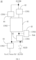
- FIG. 3 shows a circuit diagram of the switching sub-circuit 21 according to embodiments of the present disclosure.
- the switching sub-circuit 21 according to the embodiments of the present disclosure includes a first transistor T1, a second transistor T2, and a third transistor T3.
- the first transistor T1, the second transistor T2, and the third transistor T3 are all shown as N-type transistors. In other embodiments, a part or all of the first transistor T1, the second transistor T2, and the third transistor T3 may be P-type transistors.
- a gate of the first transistor T1 is electrically connected to receive the first switching signal SW1
- a first electrode of the first transistor T1 is electrically connected to receive the initialization signal Vref
- a second electrode of the first transistor T1 is electrically connected to a second electrode of the transistor T2 and serves as the output terminal Vref/Sens(k) of the switching sub-circuit 21.
- a gate of the second transistor T2 is electrically connected to receive the second switching signal SW2, and a first electrode of the second transistor T2 is electrically connected to a first electrode of the third transistor T3.
- a gate of the third transistor T3 is electrically connected to receive a sampling control signal SW3, and a second electrode of the third transistor T3 is a terminal Sens for sensing and is electrically connected to the sampling sub-circuit 22.
- the transistor T1 when the first switching signal SW1 is at a first level (for example, a high level), and the second switching signal SW2 and the sampling control signal SW3 are at a second level (for example, a low level), the transistor T1 is turned on, and the transistors T2 and T3 are turned off. At this time, the initialization signal Vref applied to the first electrode of the transistor T1 is output to the output terminal Vref/Sens(k) via the transistor T1, so that the initialization signal may be provided to the corresponding pixel driving circuit 111.
- a first level for example, a high level
- the second switching signal SW2 and the sampling control signal SW3 are at a second level (for example, a low level
- the transistor T2 When the second switching signal SW2 is at the first level (for example, the high level) and the first switching signal SW1 and the sampling control signal SW3 are at the second level (for example, the low level), the transistor T2 is turned on, and the transistors T1 and T3 are turned off. At this time, the output terminal Vref/Sens(k) may be placed in a floating state. The voltage at the first node N1 may continuously charge a lead of the output terminal Vref/Sens(k), so that the voltage at the first node N1 may be obtained at the output terminal Vref/Sens(k).
- the sampling control signal SW3 is set to the first level (for example, the high level), that is, the sampling sub-circuit 22 is communicated with the output terminal Vref/Sens(k), so that the voltage at the first node N1 may be sampled by the sampling sub-circuit 22.
- FIG. 4 shows a schematic block diagram of a pixel driving circuit according to embodiments of the present disclosure.
- the light-emitting element OLED is shown in the form of a dotted line.
- a first end of the light-emitting element OLED and the pixel driving circuit 40 are electrically connected to the first node N1, and a second end of the light-emitting element OLED is electrically connected to a fixed voltage ELVSS.
- the first end may be an anode of the light-emitting element OLED
- the second end may be a cathode of the light-emitting element OLED.
- the pixel driving circuit 40 includes a driving sub-circuit 41, and the driving sub-circuit 41 and the light-emitting element OLED are electrically connected to the first node N1 to generate a current for causing the light-emitting element OLED to emit light.
- the pixel driving circuit 40 also includes a light emission control sub-circuit 42.
- a first part of the light emission control sub-circuit 42 is electrically connected to a fixed voltage signal ELVDD (a first voltage signal) and the driving sub-circuit 41.
- a second part of the light emission control sub-circuit 42 is electrically connected to the driving sub-circuit 41 and the light-emitting element OLED.
- the light emission control sub-circuit 42 is configured to receive a first control signal CON1, and to provide the current for causing the light-emitting element OLED to emit light to the light-emitting element OLED under the control of the first control signal CON1.
- the pixel driving circuit 40 further includes a driving control sub-circuit 43, the driving control sub-circuit 43 is electrically connected to a node between the driving sub-circuit 41 and the second part of the light emission control sub-circuit 42.
- the driving control sub-circuit 43 is configured to receive the compensation data signal Da k and a second control signal CON2, and to provide the compensation data signal Da k to the driving sub-circuit 41 under the control of the second control signal CON2.
- the compensation data signal Da k is a signal provided by the first compensation sub-circuit 12.
- the pixel driving circuit 40 further includes a reset sub-circuit 44.
- a first part of the reset sub-circuit 44 is electrically connected between the driving sub-circuit 41 and the first compensation sub-circuit 12.
- the first part of the reset sub-circuit 44 and the driving sub-circuit are electrically connected to the first node N1 between the driving sub-circuit 44 and the light-emitting element OLED, and are electrically connected to the output terminal Vref/Sens(k) of the switching sub-circuit 21 in the first compensation sub-circuit 12.
- the part of the reset sub-circuit 44 is configured to receive a fourth control signal CON4, and to apply the initialization signal Vref provided by the first compensation sub-circuit 12 to the first node N1 under the control of the fourth control signal or to output the voltage at the first node N1 when the OLED emits light (that is, the voltage of the anode of the light-emitting element OLED) to the first compensation sub-circuit 12 under the control of the fourth control signal.
- a second part of the reset sub-circuit 44 is electrically connected between the first voltage signal ELVDD and the driving sub-circuit 41, and receives the fourth control signal CON4.
- the part of the reset sub-circuit 44 is configured to reset the driving sub-circuit 41 under the control of the fourth control signal.
- FIG.S 5 and 6 respectively show circuit diagrams of the pixel driving circuit 50 and the pixel driving circuit 60 according to embodiments of the present disclosure. Next, two examples according to the embodiments of the present disclosure will be described in detail with reference to FIGS. 5 and 6 .
- the driving sub-circuit 41 of the pixel driving circuit 50 includes a driving transistor DTFT, a fourth transistor T4 and a storage capacitor C1.
- a gate of the driving transistor DTFT is electrically connected to a first end of the storage capacitor C1
- a drain of the driving transistor DTFT and a first part of the light emission control sub-circuit 52 are electrically connected to a second node N2
- a source of the driving transistor DTFT and a second part of the light emission control sub-circuit 52 is electrically connected to a third node N3.
- a gate of the fourth transistor T4 is electrically connected to receive the second control signal CON2, a first electrode of the fourth transistor T4 is electrically connected to the first end of the storage capacitor C1, and a second electrode of the fourth transistor T4 is electrically connected to the second node N2.
- the first end of the storage capacitor C1 is electrically connected to the gate of the driving transistor DTFT and the first electrode of the fourth transistor T4, and the second end of C1 is electrically connected to the first node N1.
- the light emission control sub-circuit 52 of the pixel driving circuit 50 includes a fifth transistor T5 and a sixth transistor T6.
- a gate of the fifth transistor T5 is electrically connected to receive the first control signal CON1
- a first electrode of the fifth transistor T5 is electrically connected to receive the first voltage signal ELVDD
- a second electrode of the fifth transistor T5 is electrically connected to the second node N2.
- a gate of the sixth transistor T6 is electrically connected to receive the first control signal CON1
- a first electrode of the sixth transistor T6 is electrically connected to the third node N3, and a second electrode of the sixth transistor T6 is electrically connected to the first node N1.
- the driving control sub-circuit 53 of the pixel driving circuit 50 includes a seventh transistor T7.
- a gate of the seventh transistor T7 is electrically connected to receive the second control signal CON2, and a first electrode of the seventh transistor T7 is electrically connected to receive the compensation data signal Da k , and a second electrode of the seventh transistor T7 is electrically connected to the third node N3.
- the reset sub-circuit 54 of the pixel driving circuit 50 includes an eighth transistor T8 and a ninth transistor T9.
- a gate of the eighth transistor T8 is electrically connected to receive the third control signal CON3, a first electrode of the eighth transistor T8 is electrically connected to the first node N1, and a second electrode of the eighth transistor T8 is electrically connected to the first compensation sub-circuit 12, namely the output terminal Vref/Sens(k) of the switching sub-circuit 21.
- a gate of the ninth transistor T9 is electrically connected to receive the fourth control signal CON4, a first electrode of the ninth transistor T9 is electrically connected to receive the first voltage signal ELVDD, and a second electrode of the ninth transistor T9 is electrically connected to the first end of the storage capacitor C1.
- a change in the threshold voltage Vth caused by factors such as temperature drift within the driving transistor may be compensated to ensure that the DTFT outputs a stable current under different working conditions.
- changes in OLED characteristics caused by the aging of the light-emitting element OLED may be compensated to ensure the display effect of the OLED device when the OLED device is aging.
- the embodiments of the present disclosure may ensure the characteristics of the OLED device after long-term use, thereby prolonging the service life and improving image quality of the OLED display.
- Each transistor in the pixel driving circuit 50 has a parasitic capacitance. These parasitic capacitances will affect the first node N1, that is, affect the voltage of the anode of the light-emitting element OLED, thereby affecting the displayed image. Therefore, in the pixel circuit 10 according to the embodiments of the present disclosure, a second compensation sub-circuit 13 is provided.
- the second compensation sub-circuit 13 includes a plurality of compensation capacitors C2, a first end of each compensation capacitor C2 is electrically connected to the first node N1, and a second end of each compensation capacitor C2 is electrically connected to the gate of the seventh transistor T7.
- the second compensation sub-circuit 13 may reduce light leakage of the OLED device in black state.
- the compensation capacitor C2 is coupled to the anode of the light-emitting element OLED to reduce the voltage of the anode of the light-emitting element OLED during the light-emitting period, so as to prevent light leakage of the OLED device in the black state which otherwise affects the contrast.
- the pixel driving circuit 60 shown in FIG. 6 has substantially the same structure as the pixel driving circuit 50 shown in FIG. 5 .
- the difference is in that the fourth transistor and the ninth transistor both adopt dual-gate transistors.
- the fourth transistor is denoted as T4_1 and T4_2
- the ninth transistor is denoted as T9_1 and T9_2.
- the dual-gate structure of the transistor may better reduce the leakage current of the transistor, thereby helping to improve the display effect.
- transistors may also be used to implement the embodiments of the present disclosure according to specific implementation requirements and implementation processes.
- P-type or N-type LTPS, LTPO, or IGZO transistors may be included in the circuit structure. Those skilled in the art can easily understand these modified circuit structures, which will not be repeated here.
- FIG. 7 shows a flowchart of a driving method 700 of a pixel circuit according to embodiments of the present disclosure. As shown in FIG. 7 , the driving method 700 may include the following steps.
- step S710 a threshold voltage of the pixel driving circuit is compensated, so as to eliminate an influence of the threshold voltage on current flowing through the light-emitting element.
- step S720 a compensation data signal is generated by using the first compensation sub-circuit.
- step S730 the light-emitting element in each pixel unit is driven to emit light based on the compensation data signal.
- the compensation data signal before driving the light-emitting element in each pixel unit to emit light, the compensation data signal may be generated based on the light-emitting brightness of the selected light-emitting element.
- the light-emitting brightness of the selected light-emitting element may be a black-state image, and original data signals corresponding to the selected light-emitting brightness are gray scales in the black state display.
- the compensation data signal is obtained according to the original data signals, and the compensation model is selected.
- the light-emitting brightness of the selected light-emitting element may be a fixed white-state brightness, or may also be a certain selected brightness higher than the white-state brightness during normal display.
- the compensation data signal in the process of driving the light-emitting element in each pixel unit to emit light, may be generated based on the light-emitting brightness of the light-emitting element in each pixel unit. In this case, it is necessary to perform compensation for each light-emitting element during the light-emitting process of each of the light-emitting elements in the pixel units. This compensation method may more accurately compensate the aging characteristics of each light-emitting element, and may provide better display quality.
- the compensation data signal may be generated based on the light-emitting brightness of light-emitting element in each of selected pixel units during the light-emitting process of each light-emitting element in the pixel unit.
- the light-emitting brightness of the selected light-emitting elements may include a black-state image, a fixed white-state brightness, or a certain selected brightness higher than the white-state brightness during normal display.
- FIG. 8 shows a flowchart of operations 800, in a sampling period, of the driving method of a pixel circuit according to embodiments of the present disclosure
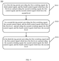
- FIG. 9 shows a flowchart of operations 900, in a driving period, of the driving method of a pixel circuit according to embodiments of the present disclosure.
- the operations 800 in which the first compensation sub-circuit is used to generate the compensation data signal in the sampling period may include the following steps.
- step S810 in a first sampling period, a second switching signal, a first control signal and a third control signal which all have a first level are provided, and a first switching signal, a sampling control signal, a second control signal and a fourth control signal which all have a second level are provided.
- step S820 in a second sampling period, the second switching signal, the sampling control signal, the first control signal, and the third control signal which all have the first level are provided, and the first switching signal, the second control signal and the fourth control signal which all have the second level are provided.
- the operations 900 in which the light-emitting element in each pixel unit is driven to emit light based on the compensation data signal in the driving period may include the following steps.
- step S910 in a first driving period, the first switching signal, the third control signal, and the fourth control signal which all have the first level are provided, and the second switching signal, the first control signal, and the second control signal which all have the second level are provided.
- step S920 in a second driving period, the first switching signal, the second control signal, and the third control signal which all have the first level are provided, and the second switching signal, the first control signal, and the fourth control signal which all have the second level are provided.
- step S930 in the third driving period, the first switching signal and the first control signal which both have the first level are provided, and the second switching signal, the second control signal, the third control signal, and the fourth control signal which all have the second level are provided.
- FIGS. 10 and 11 show timing diagrams of a driving method of a pixel circuit according to embodiments of the present disclosure. The driving method of the pixel circuit will be described below with reference to FIGS. 1 , 2 , 3 , 5 , 10 , and 11 in conjunction with specific embodiments.
- FIG. 10 it shows operation timing of the pixel driving circuit when the pixel circuit is not switched to the compensation mode, that is, when the data signal is not compensated.
- the first control signal CON1 is at a low level, so that the transistors T5 and T6 are turned off.
- the second control signal CON2 is at a low level, so that the transistors T4 and T7 are turned off.
- the first switching signal SW1 is at a high level, and the second switching signal SW2 is at a low level, so that the output terminal Vref/Sens(k) of the switching sub-circuit 21 outputs the initialization voltage Vref.
- the third control signal CON3 and the fourth control signal CON4 are at a high level.
- the first control signal CON1 is at a low level, so that the transistors T5 and T6 are kept off.
- the fourth control signal CON4 is at a low level, so that the transistor T9 is turned off.
- the first switching signal SW1 is at a high level, and the second switching signal SW2 is at a low level, therefore the output terminal Vref/Sens(k) of the switching sub-circuit 21 maintains the initializing voltage Vref.
- the second control signal CON2 is at a high level, so that the transistors T4 and T7 are turned on. Since the transistor T4 is turned on, the drain and the gate of the driving transistor DTFT are electrically connected, and the DTFT forms a diode structure.
- VDTFT_G Vdata+Vth, wherein Vth (Vth>0) is the threshold voltage of the driving transistor DTFT, and Vdata represents the uncompensated data signal, that is, in FIG 4 , what is actually received at the position where Da k is received is the uncompensated data signal Vdata.
- Vth Vth>0
- Vdata represents the uncompensated data signal, that is, in FIG 4 , what is actually received at the position where Da k is received is the uncompensated data signal Vdata.
- the third control signal CON3 is always maintained at a high level, so that the transistor T3 is maintained to be turned on, thus the anode of the switching element OLED is always maintained at the Vref potential.
- the second control signal CON2, the third control signal CON3, and the fourth control signal CON4 are at a low level, therefore the transistors T4, T7, T8, and T9 are turned off.
- the first control signal CON1 is at a high level, so the transistors T5 and T6 are turned on, and current flows through the light-emitting element OLED so that the OLED emits light.
- the first switching signal SW1 is at a high level, and the second switching signal SW2 is at a low level, so that the output terminal Vref/Sens(k) of the switching sub-circuit 21 maintains the output initialization voltage Vref.
- FIG. 11 shows operation timing for driving the light-emitting element to emit light with the compensated data signal when the pixel circuit is switched to the compensation mode.
- the operation of generating the compensation data signal based on the light-emitting brightness of the light-emitting element in each pixel unit in the process of driving the light-emitting element in each pixel unit to emit light is explained.
- the first control signal CON1 is at a low level, so that the transistors T5 and T6 are turned off.
- the second control signal CON2 is at a low level, so that the transistors T4 and T7 are turned off.
- the first switching signal SW1 is at a high level, and the second switching signal SW2 is at a low level, so that the output terminal Vref/Sens(k) of the switching sub-circuit 21 outputs the initialization voltage Vref.
- the third control signal CON3 and the fourth control signal CON4 are at a high level.
- the first control signal CON1 is at a low level, so that the transistors T5 and T6 are kept off.
- the fourth control signal CON4 is at a low level, so that the transistor T9 is turned off.
- the first switching signal SW1 is at a high level
- the second switching signal SW2 is at a low level, so that the output terminal Vref/Sens(k) of the switching sub-circuit 21 maintains the output of the initialization voltage Vref.
- the second control signal CON2 is at a high level, so that the transistors T4 and T7 are turned on. Since the transistor T4 is turned on, the drain and the gate of the driving transistor DTFT are electrically connected, and the DTFT forms a diode structure.
- VDTFT_G Vdata+Vth, wherein Vth (Vth>0) is the threshold voltage of the driving transistor DTFT, and Vdata represents the uncompensated initial data signal, which is a theoretical data signal without considering the aging of the OLED device.
- Vth Vth>0
- Vdata represents the uncompensated initial data signal, which is a theoretical data signal without considering the aging of the OLED device.
- the third control signal CON3 is always maintained at a high level, so that the transistor T3 is maintained to be turned on, so that that the anode of the switching element OLED is always maintained at the Vref potential.
- the second control signal CON2 and the fourth control signal CON4 are at low level, so that the transistors T4, T7, and T9 are turned off.
- the first switching signal SW1 and the sampling control signal SW3 are at a low level, and the second switching signal SW2 is at a high level, therefore the output terminal Vref/Sens(k) of the switching sub-circuit 21 is kept in a floating state.
- the third control signal CON3 is at a high level, so that the transistor T8 is turned on.
- the voltage at the first node N1 may be obtained at the output terminal Vref/Sens(k), that is voltage of the anode of the light-emitting element OLED.
- the first control signal CON1 is at a high level, so that the transistors T5 and T6 are turned on, and the initial data signal Vdata written in the t2 period is configured to drive the light-emitting element OLED to emit light.
- the anode of the light-emitting element OLED continuously charges Vref/Sens(k) through T8 until it reaches the voltage stabilization stage, at this time the OLED reaches the normal display brightness, and the actual voltage at the OLED anode is obtained at Vref/Sens(k).
- the first control signal CON1, the second control signal CON2, the third control signal CON3, the fourth control signal CON4, the first switching signal SW1, and the second switching signal SW2 are maintained at the same level as the s1 period.
- the sampling control signal SW3 is at a high level, and the sampling sub-circuit 22 is connected to the output terminal Vref/Sens(k) to sample the voltage at the first node N1.
- the sampling sub-circuit 22 is an analog-to-digital converter ADC
- the output terminal Vref/Sens(k) is communicated with the input terminal of the ADC device, and the ADC device reads the voltage at the first node N1, namely, the voltage of the OLED anode.
- the data compensation sub-circuit 23 may compare the collected voltage at the first node N1 with the expected voltage of the OLED under the brightness, and the compensation signal is obtained according to the compensation model in the data compensation sub-circuit 23, and further it is fed back to the data signal through gamma voltage, thereby generating a compensation data signal Da k , and applying the compensation data signal Da k to the first electrode of the transistor T7.
- the operations of the first driving period (t1 period), the second driving period (t2 period), and the third driving period (t3 period) are sequentially performed again, and the light-emitting element OLED is driven to emit light with the compensation data signal Da k , thereby realizing the compensation for the aging of OLED.
- the operations of the first driving period (t1 period), the second driving period (t2 period), and the third driving period (t3 period) reference may be made to the foregoing description, which will not be repeated here.
- the first driving period (t1 period), the second driving period (t2 period), the first sampling period (s1 period), and the second sampling period (s2 period) mentioned above may be repeated once based on the light-emitting brightness of the selected light-emitting element, so as to select a unified compensation model to compensate all light-emitting elements.
- a change in the threshold voltage Vth caused by factors such as temperature drift within the driving transistor may be compensated to ensure that the DTFT outputs a stable current under different working conditions.
- changes in OLED characteristics caused by the aging of the light-emitting element OLED may be compensated to ensure the display effect of the OLED device when the OLED device is aging.
- the embodiments of the present disclosure may ensure the characteristics of the OLED device after long-term use, thereby prolonging the service life and improving image quality of the OLED display.
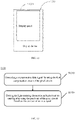
- FIG. 12 shows a schematic block diagram of a display device according to embodiments of the present disclosure
- FIG. 13 shows a flowchart of a display method of a display device according to embodiments of the present disclosure.
- a display device 1200 may include a display panel 1201, and the display panel 1201 includes a pixel circuit 10 according to embodiments of the present disclosure.
- the display device 900 may be any product or component with a display function such as electronic paper, mobile phone, tablet computer, television, display, notebook computer, digital photo frame, navigator, etc.
- the method of using the display device 1200 for display may include the following steps.
- step S1310 a compensation data signal is generated by using the first compensation sub-circuit of the pixel circuit.
- step S1320 the light-emitting element in each pixel unit is driven to emit light by using the pixel unit of the pixel circuit based on the compensation data signal.
- the first compensation sub-circuit before driving the light-emitting element in each pixel unit to emit light, the first compensation sub-circuit may be used to generate the compensation data signal based on the light-emitting brightness of the selected light-emitting element.
- the first compensation sub-circuit in the process of driving the light-emitting element in each pixel unit to emit light, may be used to generate the compensation data signal based on the light-emitting brightness of the light-emitting element in each pixel unit.
Landscapes
- Engineering & Computer Science (AREA)
- Physics & Mathematics (AREA)
- Computer Hardware Design (AREA)
- General Physics & Mathematics (AREA)
- Theoretical Computer Science (AREA)
- Control Of Indicators Other Than Cathode Ray Tubes (AREA)
Applications Claiming Priority (1)
| Application Number | Priority Date | Filing Date | Title |
|---|---|---|---|
| PCT/CN2020/082569 WO2021196015A1 (zh) | 2020-03-31 | 2020-03-31 | 像素电路及其驱动方法、显示装置及其驱动方法 |
Publications (3)
| Publication Number | Publication Date |
|---|---|
| EP4131238A1 true EP4131238A1 (de) | 2023-02-08 |
| EP4131238A4 EP4131238A4 (de) | 2023-05-17 |
| EP4131238B1 EP4131238B1 (de) | 2026-05-06 |
Family
ID=77927017
Family Applications (1)
| Application Number | Title | Priority Date | Filing Date |
|---|---|---|---|
| EP20924970.5A Active EP4131238B1 (de) | 2020-03-31 | 2020-03-31 | Pixelschaltung und ansteuerungsverfahren dafür, und anzeigevorrichtung und ansteuerungsverfahren dafür |
Country Status (4)
| Country | Link |
|---|---|
| US (1) | US11501707B2 (de) |
| EP (1) | EP4131238B1 (de) |
| CN (1) | CN113748455B (de) |
| WO (1) | WO2021196015A1 (de) |
Families Citing this family (8)
| Publication number | Priority date | Publication date | Assignee | Title |
|---|---|---|---|---|
| CN110827730B (zh) * | 2019-11-28 | 2022-12-13 | 京东方科技集团股份有限公司 | 一种检测ltpsamoled显示基板像素区晶体管特性的电路与方法 |
| CN111583872B (zh) * | 2020-06-11 | 2021-03-12 | 京东方科技集团股份有限公司 | 像素补偿装置及像素补偿方法、显示装置 |
| CN116420183B (zh) * | 2020-09-25 | 2024-12-06 | 京东方科技集团股份有限公司 | 像素电路、像素驱动方法、显示面板和显示装置 |
| CN113990262B (zh) * | 2021-11-18 | 2023-03-21 | 武汉天马微电子有限公司 | 一种像素电路、显示面板及显示装置 |
| CN114267297B (zh) * | 2021-12-16 | 2023-05-02 | Tcl华星光电技术有限公司 | 像素补偿电路、方法及显示面板 |
| US12437714B2 (en) | 2022-03-29 | 2025-10-07 | Yunnan Invensight Optoelectronics Technology Co., Ltd. | Display panel, display device, and method for compensating signal |
| WO2023226013A1 (zh) | 2022-05-27 | 2023-11-30 | 京东方科技集团股份有限公司 | 像素电路及其驱动方法、显示基板、显示装置 |
| CN119920202A (zh) * | 2023-10-31 | 2025-05-02 | 京东方科技集团股份有限公司 | 像素驱动电路及其驱动方法、显示基板和显示装置 |
Family Cites Families (29)
| Publication number | Priority date | Publication date | Assignee | Title |
|---|---|---|---|---|
| KR20120062252A (ko) | 2010-12-06 | 2012-06-14 | 삼성모바일디스플레이주식회사 | 화소 및 이를 이용한 유기전계발광 표시장치 |
| KR101493226B1 (ko) * | 2011-12-26 | 2015-02-17 | 엘지디스플레이 주식회사 | 유기 발광 다이오드 표시 장치의 화소 구동 회로의 특성 파라미터 측정 방법 및 장치 |
| KR102118926B1 (ko) * | 2013-12-23 | 2020-06-04 | 엘지디스플레이 주식회사 | 유기 발광 표시 장치 |
| KR20150138527A (ko) * | 2014-05-29 | 2015-12-10 | 삼성디스플레이 주식회사 | 화소 회로 및 이를 포함하는 전계발광 디스플레이 장치 |
| US9607549B2 (en) * | 2014-12-24 | 2017-03-28 | Lg Display Co., Ltd. | Organic light emitting diode display panel and organic light emitting diode display device |
| EP3098805B1 (de) * | 2015-05-28 | 2018-07-25 | LG Display Co., Ltd. | Organische lichtemittierende anzeige und schaltung dafür |
| KR102408900B1 (ko) * | 2015-10-23 | 2022-06-16 | 엘지디스플레이 주식회사 | 스캔 구동부, 표시장치 및 이의 구동방법 |
| CN105679236B (zh) * | 2016-04-06 | 2018-11-30 | 京东方科技集团股份有限公司 | 像素电路及其驱动方法、阵列基板、显示面板和显示装置 |
| KR102456297B1 (ko) * | 2016-04-15 | 2022-10-20 | 삼성디스플레이 주식회사 | 화소 회로 및 이의 구동 방법 |
| CN106097964B (zh) * | 2016-08-22 | 2018-09-18 | 京东方科技集团股份有限公司 | 像素电路、显示面板、显示设备及驱动方法 |
| CN107342047B (zh) * | 2017-01-03 | 2020-06-23 | 京东方科技集团股份有限公司 | 像素电路及其驱动方法、以及显示面板 |
| CN106652907B (zh) * | 2017-01-05 | 2019-02-05 | 上海天马有机发光显示技术有限公司 | 有机发光显示面板、有机发光显示装置及像素补偿方法 |
| CN107038987B (zh) * | 2017-05-23 | 2020-12-22 | 上海和辉光电股份有限公司 | 一种共栅晶体管、像素电路、驱动方法及显示器 |
| CN107038992B (zh) * | 2017-05-23 | 2019-06-18 | 上海和辉光电有限公司 | 一种像素电路、驱动方法及显示器 |
| CN107230448A (zh) * | 2017-05-23 | 2017-10-03 | 上海和辉光电有限公司 | 一种像素电路、驱动方法及显示器 |
| CN109872692B (zh) * | 2017-12-04 | 2021-02-19 | 京东方科技集团股份有限公司 | 像素电路及其驱动方法、显示装置 |
| WO2020034140A1 (en) * | 2018-08-16 | 2020-02-20 | Boe Technology Group Co., Ltd. | A method for driving a pixel circuit with feedback compensation, a circuit for driving a light-emitting device, and a display apparatus |
| CN109545146B (zh) | 2018-12-13 | 2020-07-03 | 昆山国显光电有限公司 | 一种oled显示面板驱动电路及oled显示面板 |
| CN109523950B (zh) | 2018-12-13 | 2020-09-11 | 昆山国显光电有限公司 | 一种oled显示面板驱动电路及驱动方法 |
| CN117765880A (zh) * | 2019-01-18 | 2024-03-26 | 京东方科技集团股份有限公司 | 像素电路、驱动方法、电致发光显示面板及显示装置 |
| CN109817159B (zh) * | 2019-03-29 | 2021-07-20 | 昆山国显光电有限公司 | 一种像素驱动电路以及显示装置 |
| CN110189701B (zh) * | 2019-06-28 | 2022-07-29 | 京东方科技集团股份有限公司 | 像素驱动电路及其驱动方法、显示面板与显示装置 |
| KR102736610B1 (ko) * | 2019-07-23 | 2024-12-03 | 삼성디스플레이 주식회사 | 표시 장치의 오버드라이빙 데이터 획득 방법, 표시 장치의 구동 방법, 및 표시 장치 |
| CN112309331B (zh) * | 2019-07-31 | 2026-01-23 | 京东方科技集团股份有限公司 | 一种显示面板及其控制方法、显示装置 |
| KR102575448B1 (ko) * | 2019-08-30 | 2023-09-05 | 엘지디스플레이 주식회사 | 터치표시장치 및 그 구동방법 |
| CN110634432B (zh) * | 2019-10-25 | 2023-05-12 | 京东方科技集团股份有限公司 | Oled像素电路、驱动方法、老化检测方法和显示面板 |
| CN110827757A (zh) | 2019-10-28 | 2020-02-21 | 福建华佳彩有限公司 | Oled电路补偿方法 |
| CN110853584A (zh) * | 2019-11-28 | 2020-02-28 | 京东方科技集团股份有限公司 | 像素驱动电路、显示面板及其驱动方法 |
| CN111179855B (zh) | 2020-03-18 | 2021-03-30 | 京东方科技集团股份有限公司 | 像素电路及其驱动方法、显示装置 |
-
2020
- 2020-03-31 CN CN202080000451.9A patent/CN113748455B/zh active Active
- 2020-03-31 EP EP20924970.5A patent/EP4131238B1/de active Active
- 2020-03-31 US US17/260,746 patent/US11501707B2/en active Active
- 2020-03-31 WO PCT/CN2020/082569 patent/WO2021196015A1/zh not_active Ceased
Also Published As
| Publication number | Publication date |
|---|---|
| CN113748455A (zh) | 2021-12-03 |
| WO2021196015A1 (zh) | 2021-10-07 |
| US11501707B2 (en) | 2022-11-15 |
| US20220108655A1 (en) | 2022-04-07 |
| EP4131238A4 (de) | 2023-05-17 |
| CN113748455B (zh) | 2023-11-03 |
| EP4131238B1 (de) | 2026-05-06 |
Similar Documents
| Publication | Publication Date | Title |
|---|---|---|
| EP4131238B1 (de) | Pixelschaltung und ansteuerungsverfahren dafür, und anzeigevorrichtung und ansteuerungsverfahren dafür | |
| US11984081B2 (en) | Pixel circuit and method of driving the same, display device | |
| US11030959B2 (en) | Pixel circuit and driving method thereof, and display device | |
| US11881164B2 (en) | Pixel circuit and driving method thereof, and display panel | |
| US11024229B2 (en) | Display panel and detection method thereof, and display device | |
| US11837169B2 (en) | Pixel circuit, display substrate and display apparatus | |
| US9881552B2 (en) | Display device and method for driving same | |
| US10229639B2 (en) | Pixel driving circuit for compensating drifting threshold voltage of driving circuit portion and driving method thereof | |
| CN111105751B (zh) | 显示设备、用于驱动显示设备的方法以及电子装置 | |
| EP3736800A1 (de) | Pixelschaltung und ansteuerungsverfahren dafür sowie anzeigevorrichtung | |
| US20180342208A1 (en) | Display device and method for driving same | |
| US11107408B2 (en) | Pixel circuit and driving method thereof, and display device | |
| EP3723077A1 (de) | Pixelschaltung und ansteuerungsverfahren dafür sowie anzeigevorrichtung | |
| US11282437B2 (en) | Pixel circuit and driving method thereof, and display device | |
| US20160035276A1 (en) | Oled pixel circuit, driving method of the same, and display device | |
| US20190103055A1 (en) | Pixel driving circuit and driving method thereof, display panel and display device | |
| US20170249898A1 (en) | Pixel circuit and driving method thereof, display substrate, and display apparatus | |
| EP2200010B1 (de) | Stromgesteuertes display | |
| US11881178B2 (en) | Light emitting display device and method of driving same | |
| CN111785212A (zh) | 一种像素电路、其驱动方法及显示装置 | |
| US11514844B2 (en) | Pixel drive circuit, pixel unit, driving method, array substrate, and display apparatus | |
| CN117672139A (zh) | 像素电路及其驱动方法、显示面板、显示装置 | |
| CN111029395B (zh) | 基于有机薄膜晶体管的电流型像素驱动电路 | |
| US20220208098A1 (en) | Data current generation circuit, driving method, driver chip and display panel |
Legal Events
| Date | Code | Title | Description |
|---|---|---|---|
| STAA | Information on the status of an ep patent application or granted ep patent |
Free format text: STATUS: UNKNOWN |
|
| STAA | Information on the status of an ep patent application or granted ep patent |
Free format text: STATUS: THE INTERNATIONAL PUBLICATION HAS BEEN MADE |
|
| PUAI | Public reference made under article 153(3) epc to a published international application that has entered the european phase |
Free format text: ORIGINAL CODE: 0009012 |
|
| STAA | Information on the status of an ep patent application or granted ep patent |
Free format text: STATUS: REQUEST FOR EXAMINATION WAS MADE |
|
| 17P | Request for examination filed |
Effective date: 20210920 |
|
| AK | Designated contracting states |
Kind code of ref document: A1 Designated state(s): AL AT BE BG CH CY CZ DE DK EE ES FI FR GB GR HR HU IE IS IT LI LT LU LV MC MK MT NL NO PL PT RO RS SE SI SK SM TR |
|
| A4 | Supplementary search report drawn up and despatched |
Effective date: 20230418 |
|
| RIC1 | Information provided on ipc code assigned before grant |
Ipc: G09G 3/3233 20160101AFI20230412BHEP |
|
| DAV | Request for validation of the european patent (deleted) | ||
| DAX | Request for extension of the european patent (deleted) | ||
| STAA | Information on the status of an ep patent application or granted ep patent |
Free format text: STATUS: EXAMINATION IS IN PROGRESS |
|
| 17Q | First examination report despatched |
Effective date: 20240816 |
|
| GRAP | Despatch of communication of intention to grant a patent |
Free format text: ORIGINAL CODE: EPIDOSNIGR1 |
|
| STAA | Information on the status of an ep patent application or granted ep patent |
Free format text: STATUS: GRANT OF PATENT IS INTENDED |
|
| GRAS | Grant fee paid |
Free format text: ORIGINAL CODE: EPIDOSNIGR3 |
|
| INTG | Intention to grant announced |
Effective date: 20260227 |
|
| GRAA | (expected) grant |
Free format text: ORIGINAL CODE: 0009210 |
|
| STAA | Information on the status of an ep patent application or granted ep patent |
Free format text: STATUS: THE PATENT HAS BEEN GRANTED |
|
| AK | Designated contracting states |
Kind code of ref document: B1 Designated state(s): AL AT BE BG CH CY CZ DE DK EE ES FI FR GB GR HR HU IE IS IT LI LT LU LV MC MK MT NL NO PL PT RO RS SE SI SK SM TR |
|
| REG | Reference to a national code |
Ref country code: CH Ref legal event code: F10 Free format text: ST27 STATUS EVENT CODE: U-0-0-F10-F00 (AS PROVIDED BY THE NATIONAL OFFICE) Effective date: 20260506 Ref country code: GB Ref legal event code: FG4D |